

Page 1

_______________General Description
The single MAX4112/MAX4113, dual MAX4117/
MAX4118, and quad MAX4119/MAX4120 current feedback amplifiers combine high-speed performance with
low-power operation. The MAX4112/MAX4117/
MAX4119 are optimized for closed-loop gains of 2V/V
or greater, while the MAX4113/MAX4118/MAX4120 are
optimized for gains of 8V/V or greater.
The MAX4112/MAX4117/MAX4119 and the MAX4113/
MAX4118/MAX4120 require only 5mA of supply current
per channel, and deliver 0.1dB gain flatness up to 115MHz
and -3db bandwidths of 400MHz (AV≥ 2V/V) and 300MHz
(AV≥ 8V/V), respectively. Their high slew rates of up t o
1800V/µs provide exceptional full-power bandwidths up
to 280MHz, making these amplifiers ideal for high-performance pulse and RGB video applications.
These high-speed op amps have a wide output voltage
swing of ±3.5V into 100Ω and a high current-drive
capability of 80mA.
________________________Applications
Broadcast and High-Definition TV Systems
RGB Video
Pulse/RF Amplifier
Ultrasound/Medical Imaging
Active Filters
High-Speed ADC Buffers
Professional Cameras
High-Definition Surveillance
____________________________Features
♦ 400MHz -3dB Bandwidth (MAX4112/MAX4117)
270MHz -3dB Bandwidth (MAX4113/MAX4119)
300MHz -3dB Bandwidth (MAX4118/MAX4120)
♦ 0.1dB Gain Flatness to 115MHz
♦ 1200V/µs Slew Rate
(MAX4112/MAX4117/MAX4119)
1800V/µs Slew Rate
(MAX4113/MAX4118/MAX4120)
♦ 280MHz Full-Power Bandwidth
(VO= 2Vp-p, MAX4112/MAX4117)
240MHz Full-Power Bandwidth
(VO= 2Vp-p, MAX4113/MAX4118/MAX4120)
♦ High Output Drive: 80mA
♦ Low Power: 5mA Supply Current per Channel
MAX4112/MAX4113/MAX4117–MAX4120
Single/Dual/Quad, 400MHz, Low-Power,
Current Feedback Amplifiers
________________________________________________________________
Maxim Integrated Products
1
For free samples & the latest literature: http://www.maxim-ic.com, or phone 1-800-998-8800
19-0440; Rev 2; 4/97
PART
MAX4112ESA
MAX4112EUA -40°C to +85°C
-40°C to +85°C
TEMP. RANGE PIN-PACKAGE
8 SO
8 µMAX*
______________Ordering Information
Ordering Information continued at end of data sheet.
*
Contact factory for µMAX package availability.
OUT
IN+
N.C.
V
EE
1
2
8
7
N.C.
V
CC
IN-
N.C.
MAX4112
MAX4113
SO/µMAX
TOP VIEW
3
4
6
5
INB-
INA+
INB+
V
EE
1
2
8
7
V
CC
OUTB
INA-
OUTA
MAX4117
MAX4118
SO
3
4
6
5
14
13
12
11
10
9
8
1
2
3
4
5
6
7
OUTD
INDIND+
V
EE
V
CC
INA+
INA-
OUTA
INC+
INCOUTCOUTB
INB-
INB+
SO
16
15
14
13
12
11
10
9
1
2
3
4
5
6
7
8
OUTA OUTD
INDIND+
V
EE
INC+
INCOUTC
N.C.
QSOP
INA-
INA+
INB-
V
CC
INB+
OUTB
N.C.
MAX4119
MAX4120
MAX4119
MAX4120
__________________________________________________________Pin Configurations
EVALUATION KIT
AVAILABLE
MAX4113ESA
-40°C to +85°C 8 SO
MAX4117ESA
-40°C to +85°C 8 SO
MAX4118ESA
-40°C to +85°C 8 SO
Page 2
MAX4112/MAX4113/MAX4117–MAX4120
Single/Dual/Quad, 400MHz, Low-Power,
Current Feedback Amplifiers
2 _______________________________________________________________________________________
ABSOLUTE MAXIMUM RATINGS
ELECTRICAL CHARACTERISTICS
(VCC= +5V, VEE= -5V, TA= T
MIN
to T
MAX
, unless otherwise noted. Typical values are at TA= +25°C.) (Note 1)
Stresses beyond those listed under “Absolute Maximum Ratings” may cause permanent damage to the device. These are stress ratings only, and functional
operation of the device at these or any other conditions beyond those indicated in the operational sections of the specifications is not implied. Exposure to
absolute maximum rating conditions for extended periods may affect device reliability.
Power-Supply Voltage (VCCto VEE).......................................12V
Input Voltage (IN_+, IN_-)...................(V
CC
+ 0.3V) to (VEE- 0.3V)
IN_ _ Current (Note 1)......................................................±10mA
Short-Circuit Duration (V
OUT
to GND)
V
IN
< 1.5V ...............................................................Continuous
V
IN
> 1.5V..........................................................................0sec
Continuous Power Dissipation (T
A
= +70°C)
8-Pin SO (derate 5.88mW/°C above +70°C).................471mW
8-Pin µMAX (derate 4.10mW/°C above +70°C)............330mW
14-Pin SO (derate 8.33mW/°C above +70°C)...............667mW
16-Pin QSOP (derate 9.52mW/°C above +70°C)..........762mW
Operating Temperature Range
MAX41_ _E_ _...................................................-40°C to +85°C
Storage Temperature Range.............................-65°C to +160°C
Lead Temperature (soldering, 10sec).............................+300°C
IN+ kΩ500
V
OUT
= 0V
MAX4112/MAX4117/
MAX4119
V
OUT
= 0V
RL= 30Ω, TA= 0°C to +85°C
IN-
VIN= 0V
f = 10kHz
f = 10kHz
V
OUT
= ±2.0V, VCM= 0V, RL= 100Ω
VS= ±4.5V to ±5.5V
f = 1MHz to 100MHz
f = 10kHz
V
OUT
= 0V, VIN= -V
OS
V
OUT
= 0V, VIN= -V
OS
VCM= ±2.5V
CONDITIONS
Ω30
9
Input Resistance
i
n+
Positive Input Current Noise
MAX4113/MAX4118/
MAX4120
mA65 80I
OUT
Output Current Drive
RL= 100Ω
RL= ∞
mA5 6.5I
SY
Quiescent Supply Current
per Amplifier
kΩZ
OL
Open-Loop Transimpedance 250 500
V
dB
dB45 50CMRCommon-Mode Rejection
V-2.5 2.5V
CM
Common-Mode Input Voltage
µV/°C10TCV
OS
Input Offset Voltage Drift
mV1 8V
OS
Input Offset Voltage
pA/√Hz
14i
n-
Negative Input Current Noise
pA/√Hz
13
µV
RMS
27E
nRMS
Integrated Voltage Noise
nV/√Hz
2.2e
n
Input Voltage Noise
µA3.5 20I
B+
Positive Input Bias Current
µA3.5 20I
B-
Negative Input Bias Current
UNITSMIN TYP MAXSYMBOLPARAMETER
60 80PSRPower-Supply Rejection
±3.1 ±3.5
V
OUT
Output Voltage Swing
±3.5 ±3.8
V
OUT
≤ 0.1V
RMS
MHz
400
BW
SS
Small Signal -3dB Bandwidth
300
270
MAX4112/MAX4117
MAX4113/MAX4119
MAX4118/MAX4120
DC SPECIFICATIONS (RL= ∞, unless otherwise noted)
AC SPECIFICATIONS (RL= 100Ω, unless otherwise noted)
Page 3
ELECTRICAL CHARACTERISTICS (continued)
(VCC= +5V, VEE= -5V, TA= T
MIN
to T
MAX
, unless otherwise noted. Typical values are at TA= +25°C.) (Note 1)
MAX4112/MAX4113/MAX4117–MAX4120
Single/Dual/Quad, 400MHz, Low-Power,
Current Feedback Amplifiers
_______________________________________________________________________________________ 3
Note 1: The MAX4112/MAX4113/MAX4117–MAX4120 are designed to operate in a closed-loop configuration in which the IN- pin is
driven by the OUT pin through an external feedback network. If an external voltage source is connected to IN-, current into
or out of IN- must be limited to ±10mA, to prevent damage to the part.
to 0.01%,
-1V ≤ V
OUT
≤ 1V
to 0.1%,
-1V ≤ V
OUT
≤ 1V
V
OUT
= 2Vp-p
-2V ≤ V
OUT
≤ 2V
MAX4112/MAX4117/MAX4119, A
VCL
= +2
MAX4113/MAX4118/MAX4120, A
VCL
= +8
3
ns
25
t
S
Settling Time
35
10
15
V/µs
1800
SRSlew Rate
1200
MHzBW
LS
Large-Signal -3dB Bandwidth
240
280
100
MHz
115
BW
0.1dB
0.1dB Gain Flatness
UNITSMIN TYP MAXSYMBOLPARAMETER
fC= 5MHz,
V
OUT
= 2Vp-p
f = 3.58MHz,
RL= 150Ω
f = 3.58MHz,
RL= 150Ω
dB-75Crosstalk
dB36IP3Two-Tone Third-Order Intercept
dBc
-62
SFDRSpurious-Free Dynamic Range
-68
Ω0.9Z
OUT
Output Impedance
pF2C
IN
Input Capacitance
degrees
0.04
DPDifferential Phase
0.03
%
0.02
DGDifferential Gain
0.02
ns
0.8
tR, t
F
Rise/Fall Times
10% to 90%, -2V ≤ V
OUT
≤ 2V
MAX4113/MAX4118/
MAX4120
MAX4112/MAX4117/
MAX4119
MAX4113/MAX4118/
MAX4120
MAX4112/MAX4117/
MAX4119
MAX4113/MAX4118/
MAX4120
MAX4113/MAX4118/
MAX4120
MAX4112/MAX4117
MAX4112/MAX4117/
MAX4119
CONDITIONS
All hostile, VIN= 1Vp-p, f = 10MHz
MAX4112/MAX4117/MAX4119, fC= 10MHz,
fC1= 10.1MHz, A
VCL
= +2
MAX4113/MAX4118/
MAX4120, A
VCL
= +8
MAX4112/MAX4117/
MAX4119, A
VCL
= +2
f = 10MHz, A
VCL
= +2
MAX4113/MAX4118/
MAX4120, A
VCL
= +8
MAX4113/MAX4118/
MAX4120, A
VCL
= +8
MAX4112/MAX4117/
MAX4119, A
VCL
= +2
MAX4112/MAX4117/
MAX4119, A
VCL
= +2
10% to 90%, -50mV ≤ V
OUT
≤ 50mV
MAX4119 145
AC SPECIFICATIONS (RL= 100Ω, unless otherwise noted) (continued)
Page 4
MAX4112/MAX4113/MAX4117–MAX4120
Single/Dual/Quad, 400MHz, Low-Power,
Current Feedback Amplifiers
4 _______________________________________________________________________________________
__________________________________________Typical Operating Characteristics
(VCC= +5V, VEE= -5V, RF= 499Ω, RL= 100Ω, TA = +25°C, unless otherwise noted.)
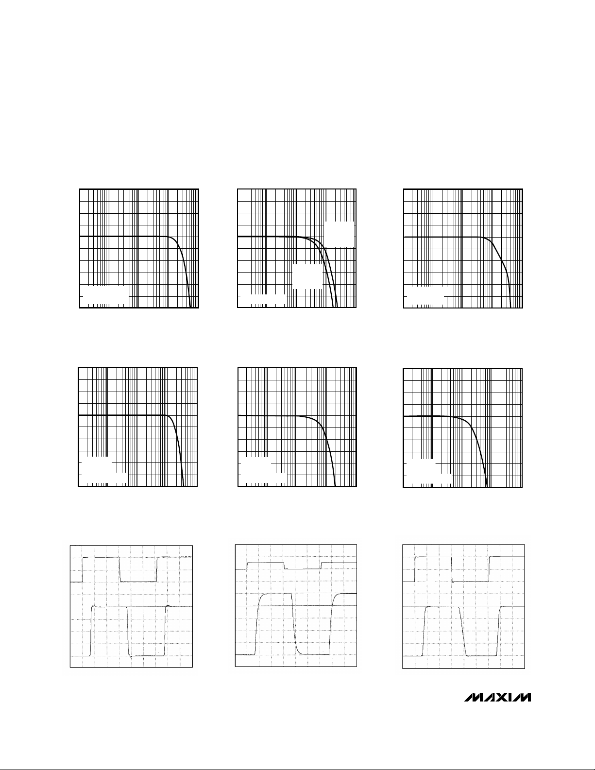
0.1 101 100 1000
MAX4112/MAX4117/MAX4119
SMALL-SIGNAL GAIN vs. FREQUENCY
(A
VCL
= +2)
MAX4112/4113-01
FREQUENCY (MHz)
NORMALIZED GAIN (dB)
-6
-5
-3
-4
-1
-2
0
1
2
4
3
V
OUT
≤ 100mVp-p
RF = RG = 600Ω
MAX4112/MAX4117/MAX4119
LARGE-SIGNAL GAIN vs. FREQUENCY
(A
VCL
= +2)
MAX4112/4113-02
0.1 101 100 1000
FREQUENCY (MHz)
NORMALIZED GAIN (dB)
-6
-5
-3
-4
-1
-2
0
1
2
4
3
V
OUT
= 2Vp-p
RF = RG = 600Ω
MAX4113/MAX4118/MAX4120
SMALL-SIGNAL GAIN vs. FREQUENCY
(A
VCL
= +8)
MAX4112/4113-03
0.1 101 100 1000
FREQUENCY (MHz)
NORMALIZED GAIN (dB)
-6
-5
-3
-4
-1
-2
0
1
2
4
3
RF = 500Ω
R
G
= 68Ω
V
OUT
≤ 100mVp-p
MAX4113/MAX4118/MAX4120
SMALL-SIGNAL GAIN vs. FREQUENCY
(A
VCL
= +20)
MAX4112/4113-4a
0.1 101 100 1000
FREQUENCY (MHz)
NORMALIZED GAIN (dB)
-6
-5
-3
-4
-1
-2
0
1
2
4
3
RF = 330Ω
R
G
= 18Ω
V
OUT
≤ 100mVp-p
IN
OUT
GND
GND
MAX4112/MAX4117/MAX4119
SMALL-SIGNAL PULSE RESPONSE
(A
VCL
= +10)
MAX4112-07
TIME (10ns/div)
VOLTAGE (20mV/div)
IN
OUT GND
GND
MAX4112/MAX4117/MAX4119
SMALL-SIGNAL PULSE RESPONSE
(A
VCL
= +2)
MAX4112-05
TIME (10ns/div)
VOLTAGE (25mV/div)
MAX4113/MAX4118/MAX4120
SMALL-SIGNAL GAIN vs. FREQUENCY
(A
VCL
= +50)
MAX4112/4113-4b
0.1 101 100 1000
FREQUENCY (MHz)
NORMALIZED GAIN (dB)
-6
-5
-3
-4
-1
-2
0
1
2
4
3
RF = 330Ω
R
G
= 6.8Ω
V
OUT
≤ 100mVp-p
IN
OUT
GND
GND
MAX4112/MAX4117/MAX4119
LARGE-SIGNAL PULSE RESPONSE
(A
VCL
= +2)
MAX4112-08
TIME (10ns/div)
VOLTAGE (1V/div)
MAX4112/MAX4117/MAX4119
SMALL-SIGNAL GAIN vs. FREQUENCY
(A
VCL
= +5, +10)
MAX4112-insert A
0.1 101 100 1000
FREQUENCY (MHz)
NORMALIZED GAIN (dB)
-6
-5
-3
-4
-1
-2
0
1
2
4
3
V
OUT
≤ 100mVp-p
AV = +5V/V
R
F
= 499Ω
R
G
= 124Ω
AV = +10V/V
R
F
= 499Ω
R
G
= 54.9Ω
Page 5

MAX4112/MAX4113/MAX4117–MAX4120
Single/Dual/Quad, 400MHz, Low-Power,
Current Feedback Amplifiers
_______________________________________________________________________________________
5
IN
OUT
GND
GND
MAX4112/MAX4117/MAX4119
LARGE-SIGNAL PULSE RESPONSE
(A
VCL
= +10)
MAX4112-10
TIME (10ns/div)
VOLTAGE (1V/div)
IN
OUT
GND
GND
MAX4112/MAX4117/MAX4119
SMALL-SIGNAL PULSE RESPONSE
(A
VCL
= +2, CL = 10pF)
MAX4112-12
TIME (10ns/div)
VOLTAGE (50mV/div)
IN
OUT
GND
GND
MAX4113/MAX4118/MAX4120
SMALL-SIGNAL PULSE RESPONSE
(A
VCL
= +8)
MAX4112-13
TIME (10ns/div)
VOLTAGE (20mV/div)
IN
OUT
GND
GND
MAX4113/MAX4118/MAX4120
LARGE-SIGNAL PULSE RESPONSE
(A
VCL
= +20)
MAX4112-16
TIME (10ns/div)
VOLTAGE (1V/div)
IN
OUT
GND
GND
MAX4113/MAX4118/MAX4120
SMALL-SIGNAL PULSE RESPONSE
(A
VCL
= +20)
MAX4112-14
TIME (10ns/div)
VOLTAGE (20mV/div)
IN
OUT
GND
GND
MAX4113/MAX4118/MAX4120
LARGE-SIGNAL PULSE RESPONSE
(A
VCL
= +8)
MAX4112-15
TIME (10ns/div)
VOLTAGE (1V/div)
30
20
10
0
2 4 6 8 10
MAX4112/MAX4117/MAX4119
SETTLING TIME vs. GAIN
MAX4112/4113 -17a
GAIN (V/V)
SETTLING TIME (ns)
-120
-110
-90
-100
-70
-80
-60
-50
-40
-20
-30
0.1 101 100
MAX4117–MAX4120
CROSSTALK vs. FREQUENCY
MAX4112/4113-18a
FREQUENCY (MHz)
AMPLITUDE (dB)
40
35
30
25
20
15
10
8 16 24 32 40 48 56
MAX4113/MAX4118/MAX4120
SETTLING TIME vs. GAIN
MAX4112/4113 -17b
GAIN (V/V)
SETTLING TIME (ns)
____________________________Typical Operating Characteristics (continued)
(VCC= +5V, VEE= -5V, RF= 499Ω, RL= 100Ω, TA = +25°C, unless otherwise noted.)
Page 6

0
-100
-80
-20
MAX4112/4113-27
LOAD RESISTANCE (Ω)
HARMONIC DISTORTION (dBc)
-40
-60
-90
-70
-10
-30
-50
3rd
A
VCL
= +2
V
OUT
= 2Vp-p
2nd
MAX4112/MAX4117/MAX4119
5MHz HARMONIC DISTORTION
vs. LOAD RESISTANCE
0 600 1000400 800200
MAX4112/MAX4113/MAX4117–MAX4120
Single/Dual/Quad, 400MHz, Low-Power,
Current Feedback Amplifiers
6 _______________________________________________________________________________________
____________________________Typical Operating Characteristics (continued)
(VCC= +5V, VEE= -5V, RF= 499Ω, RL= 100Ω, TA = +25°C, unless otherwise noted.)
1
10
100
100k10k1k100101 10M1M
INPUT VOLTAGE NOISE
vs. FREQUENCY
MAX4112/4113-19
FREQUENCY (Hz)
NOISE (nV/√Hz)
MAX4112/MAX4117/MAX4119
MAX4113/MAX4118/MAX4120
10
100
1000
100k10k1k100101 10M1M
MAX4112/MAX4117/MAX4119
INPUT CURRENT NOISE vs. FREQUENCY
MAX4112/4113-20
FREQUENCY (Hz)
NOISE (pA/√Hz)
IN+, IN-
1
10
1000
100
100k10k1k100101 10M1M
MAX4113/MAX4118/MAX4120
INPUT CURRENT NOISE vs. FREQUENCY
MAX4112/4113-21
FREQUENCY (Hz)
NOISE (pA/√Hz)
IN+
IN-
1000
100
10
1
0.1
0.1 101 100 500
CLOSED-LOOP OUTPUT IMPEDANCE
vs. FREQUENCY
MAX4112/4113-22
FREQUENCY (MHz)
OUTPUT IMPEDANCE (Ω)
-100
-90
-80
-70
-60
-50
-40
-30
-20
-10
0
0.1 1 10 100
MAX4112/MAX4117/MAX4119
HARMONIC DISTORTION vs. FREQUENCY
MAX4112/4113-23
FREQUENCY (MHz)
HARMONIC DISTORTION (dBc)
2nd
(A
VCL
= +5)
V
OUT
= 2Vp-p
2nd
(A
VCL
= +2)
3rd
(A
VCL
= +2,
A
VCL
= +5)
-100
-90
-80
-70
-60
-50
-40
-30
-20
-10
0
0.1 1 10 100
MAX4113/MAX4118/MAX4120
HARMONIC DISTORTION vs. FREQUENCY
MAX4112/4113-24
FREQUENCY (MHz)
HARMONIC DISTORTION (dBc)
3rd
(A
VCL
= +8)
3rd
(A
VCL
= +20)
2nd
(A
VCL
= +8)
2nd
(A
VCL
= +20)
V
OUT
= 2Vp-p
0
0.5 1.0 1.5 2.0 2.5 3.0 3.5 4.0
MAX4112/MAX4117/MAX4119
5MHz HARMONIC DISTORTION
vs. OUTPUT SWING
-80
-20
MAX4112/4113 -26
OUTPUT SWING (Vp-p)
HARMONIC DISTORTION (dBc)
-40
-60
-90
-70
-10
-30
-50
3rd
2nd
A
VCL
= +2
-5
15
35
55
75
95
105
0.1 101 100 1000
POWER-SUPPLY REJECTION
vs. FREQUENCY
MAX4112/4113-18b
FREQUENCY (MHz)
POWER-SUPPLY REJECTION (dB)
Page 7

MAX4112/MAX4113/MAX4117–MAX4120
Single/Dual/Quad, 400MHz, Low-Power,
Current Feedback Amplifiers
_______________________________________________________________________________________
7
0
-100
0.5 1.0 1.5 2.0 2.5 3.0 3.5 4.0
MAX4113/MAX4118/MAX4120
5MHz HARMONIC DISTORTION
vs. OUTPUT SWING
-80
-20
MAX4112/4113-28
OUTPUT VOLTAGE SWING (Vp-p)
HARMONIC DISTORTION (dBc)
-40
-60
-90
-70
-10
-30
-50
3rd
2nd
A
VCL
= +8
0
-100
0 600 1000
MAX4113/MAX4118/MAX4120
5MHz HARMONIC DISTORTION
vs. LOAD RESISTANCE
-80
-20
MAX4112/4113-29
LOAD RESISTANCE (Ω)
HARMONIC DISTORTION (dBc)
400 800200
-40
-60
-90
-70
-10
-30
-50
3rd
2nd
A
VCL
= +8
V
OUT
= 2Vp-p
0
5
10
15
20
25
30
35
40
0.1 1 10 100
TWO-TONE THIRD-ORDER INTERCEPT
vs. FREQUENCY
MAX4112/4113-30
FREQUENCY (MHz)
THIRD-ORDER INTERCEPT (dBm)
MAX4113/MAX4118/MAX4120
MAX4112/MAX4117/MAX4119
900
800
700
600
500
400
300
200
-75 -50 -25 0 25 50 75 100 125
OPEN-LOOP TRANSIMPEDANCE
vs. TEMPERATURE
MAX4112/4113-33
TEMPERATURE (°C)
TRANSIMPEDANCE (kΩ)
MAX4112/MAX4117/MAX4119
MAX4113/MAX4118/MAX4120
4.40
4.20
4.00
3.80
3.60
3.40
3.20
3.00
POSITIVE OUTPUT VOLTAGE SWING
vs. TEMPERATURE
MAX4112/4113-34a
TEMPERATURE (°C)
OUTPUT VOLTAGE SWING (V)
RL = ∞
RL = 100Ω
-75 -50 -25 0 25 50 75 100 125
0.005
0.000
-0.005
-0.010
-0.015
-0.020
-0.025
0
IRE
IRE
R
L
= 150Ω
R
L
= 150Ω
100
MAX4112/4113-31
GAIN (%)
0.00
0.01
0.02
0.03
0.04
-0.01
0 100
PHASE (degrees)
MAX4112/MAX4117/MAX4119
DIFFERENTIAL GAIN and PHASE
MAX4113/MAX4118/MAX4120
DIFFERENTIAL GAIN and PHASE
-0.005
0.000
0.005
0.010
0.015
0.020
0.025
0
IRE
IRE
100
MAX4112/4113-32
GAIN (%)
0.00
0.02
0.04
-0.06
-0.04
-0.02
0 100
PHASE (degrees)
RL = 150Ω
R
L
= 150Ω
-4.40
-4.20
-4.00
-3.80
-3.60
-3.40
-3.20
-3.00
NEGATIVE OUTPUT VOLTAGE SWING
vs. TEMPERATURE
MAX4112/4113-34b
TEMPERATURE (°C)
OUTPUT VOLTAGE SWING (V)
RL = 100Ω
RL = ∞
-75 -50 -25 0 25 50 75 100 125
-2.00
-2.50
-3.00
-3.50
-4.00
-4.50
-5.00
POSITIVE INPUT BIAS CURRENT
vs. TEMPERATURE
MAX4112/4113-35a
TEMPERATURE (°C)
INPUT BIAS CURRENT (µA)
-75 -50 -25 0 25 50 75 100 125
____________________________Typical Operating Characteristics (continued)
(VCC= +5V, VEE= -5V, RF= 499Ω, RL= 100Ω, TA = +25°C, unless otherwise noted.)
Page 8

MAX4112/MAX4113/MAX4117–MAX4120
Single/Dual/Quad, 400MHz, Low-Power,
Current Feedback Amplifiers
8 _______________________________________________________________________________________
____________________________Typical Operating Characteristics (continued)
(VCC= +5V, VEE= -5V, RF= 499Ω, RL= 100Ω, TA = +25°C, unless otherwise noted.)
-1
0
1
2
3
INPUT OFFSET VOLTAGE
vs. TEMPERATURE
MAX4112/4113 -37
TEMPERATURE (°C)
VOLTAGE (mV)
-75 -50 -25 0 25 50 75 100 125
-8.00
-6.00
-4.00
-2.00
0
2.00
4.00
6.00
8.00
POWER-SUPPLY CURRENT
vs. TEMPERATURE
(PER AMPLIFIER)
MAX4112/4113-38
TEMPERATURE (°C)
CURRENT (mA)
I
CC
I
EE
-75 -50 -25 0 25 50 75 100 125
0
1
2
3
4
5
6
7
8
NEGATIVE INPUT BIAS (IB-)
CURRENT vs. TEMPERATURE
MAX4112/4113-36
TEMPERATURE (°C)
INPUT BIAS CURRENT (µA)
-75 -50 -25 0 25 50 75 100 125
7.5
7.0
6.5
6.0
5.5
5.0
4.5
4.0
3.5
25 50 75 100 125 150
OUTPUT SWING
vs. LOAD RESISTANCE
MAX4112/4113-39
LOAD RESISTANCE (Ω)
OUTPUT SWING (Vp-p)
3.0
Page 9

FUNCTION
_____________________________________________________________Pin Descriptions
_______________Detailed Description
The MAX4112/MAX4117/MAX4119 are optimized for
closed-loop gains (A
VCL
) of 2V/V or greater, while the
MAX4113/MAX4118/MAX4120 are optimized for
closed-loop gains of 8V/V or greater. These low-power,
high-speed, current feedback amplifiers operate from
±5V supplies. They are designed to drive video loads
with low distortion characteristics. The MAX4112/
MAX4117/MAX4119’s differential gain and phase are
0.02% and 0.03°, respectively; the MAX4113/
MAX4118/MAX4120 exhibit gain/phase error specifications of 0.02% and 0.04°, respectively. These characteristics, plus a wide 0.1dB gain flatness, make the
MAX4112/MAX4113/MAX4117–MAX4120 ideal for use
in broadcast and graphics video systems. The combination of ultra-high speed and low power makes these
parts suitable for use in general-purpose, high-speed
applications, such as medical imaging, industrial instrumentation, and communications systems.
__________Applications Information
Theory of Operation
Since these devices are current-feedback amplifiers,
their open-loop transfer function is expressed as a
transimpedance, ∆V
OUT
/∆IIN, or ZOL. The frequency
behavior of the open-loop transimpedance is similar to
the open-loop gain of a voltage feedback amplifier.
That is, it has a large DC value and decreases at
approximately 6dB per octave.
Analyzing the follower with gain, as shown in Figure 1,
yields the following transfer function:
where G = A
VCL
= 1 + (RF/ RG), and RIN= 1 /gM≅ 30Ω.
V
V
G x
Z
Z G x R R
OUT
IN
OL S
OL S IN F
=
+ +
( )
( )
( )
MAX4112/MAX4113/MAX4117–MAX4120
Single/Dual/Quad, 400MHz, Low-Power,
Current Feedback Amplifiers
_______________________________________________________________________________________ 9
V
IN
R
G
R
IN
Z
OL
R
F
+1
+1
V
OUT
MAX4112
MAX4113
MAX4117
MAX4118
MAX4119
MAX4120
Figure 1. Current Feedback Amplifier
PIN
NAME FUNCTION
MAX4112
MAX4113
SO/µMAX
MAX4117
MAX4118
SO
1, 5, 8 — N.C.
No Connection. Not internally
connected.
— 1 OUTA Amplifier A Output
2 — IN- Inverting Input
— 2 INA- Amplifier A Inverting Input
3 — IN+ Noninverting Input
— 3 INA+ Amplifier A Noninverting Input
4 4 V
EE
Negative Power Supply.
Connect to -5V.
— 5 INB+ Amplifier B Noninverting Input
6 — OUT Amplifier Output
— 6 INB- Amplifier B Inverting Input
— 7 OUTB Amplifier B Output
7 8 V
CC
Positive Power Supply.
Connect to +5V.
PIN
NAME FUNCTION
1 1 OUTA Amplifier A Output
2 2 INA- Amplifier A Inverting Input
3 3 INA+ Amplifier A Noninverting Input
4 4 V
CC
Positive Power Supply.
Connect to +5V.
5 5 INB+ Amplifier B Noninverting Input
6 6 INB- Amplifier B Inverting Input
7 7 OUTB Amplifier B Output
— 8, 9 N.C.
No Connection. Not internally
connected.
8 10 OUTC Amplifier C Output
9 11 INC- Amplifier C Inverting Input
10 12 INC+ Amplifier C Noninverting Input
11 13 V
EE
Negative Power Supply.
Connect to -5V.
12 14 IND+ Amplifier D Noninverting Input
13 15 IND- Amplifier D Inverting Input
14 16 OUTD Amplifier D Output
SO QSOP
MAX4119/MAX4120
Page 10

MAX4112/MAX4113/MAX4117–MAX4120
Single/Dual/Quad, 400MHz, Low-Power,
Current Feedback Amplifiers
10 ______________________________________________________________________________________
At low gains, G x RIN<< RF. Therefore, the closed-loop
bandwidth is essentially independent of closed-loop
gain. Similarly, ZOL>> RFat low frequencies, so that:
Layout and Power-Supply Bypassing
The MAX4112/MAX4113/MAX4117–MAX4120 have an
RF bandwidth and consequently require careful board
layout, including the possible use of constant-impedance
microstrip or stripline techniques.
To realize the full AC performance of these high-speed
amplifiers, pay careful attention to power-supply
bypassing and board layout. The PC board should
have at least two layers: a signal and power layer on
one side, and a large, low-impedance ground plane on
the other side. The ground plane should be as free of
voids as possible. With multilayer boards, locate the
ground plane on a layer that incorporates no signal or
power traces.
Regardless of whether a constant-impedance board is
used, observe the following guidelines when designing
the board. Wire-wrapped boards are much too inductive, and breadboards are much too capacitive; neither
should be used. IC sockets increase parasitic capacitance and inductance, and should not be used. In general, surface-mount components give better highfrequency performance than through-hole components.
They have shorter leads and lower parasitic reactances. Keep lines as short and as straight as possible.
Do not make 90° turns; round all corners.
Observe high-frequency bypassing techniques to
maintain the amplifier’s accuracy. The bypass capacitors should include a 1000pF ceramic capacitor
between each supply pin and the ground plane, located as close to the package as possible. Next, place a
0.01µF to 0.1µF ceramic capacitor in parallel with each
1000pF capacitor, and as close to them as possible.
Then place a 10µF to 15µF low-ESR tantalum at the
point of entry (to the PC board) of the power-supply
pins. The power-supply trace should lead directly from
the tantalum capacitor to the V
CC
and VEEpins. To
minimize parasitic inductance, keep PC traces short
and use surface-mount components.
V
V
G 1 R / R
OUT
IN
F G
= = +
( )
V
OUT
R
G
V
OUT
= -(RF/RG) x V
IN
V
IN
R
F
R
O
R
S
R
T
MAX4112
MAX4113
MAX4117
MAX4118
MAX4119
MAX4120
Figure 2a. Inverting Gain Configuration
V
OUT
V
IN
R
G
V
OUT
= [1+ (RF/RG)] x V
IN
R
F
R
O
R
T
MAX4112
MAX4113
MAX4117
MAX4118
MAX4119
MAX4120
Figure 2b. Noninverting Gain Configuration
100
49.9
400
49.9
600
600
1000.1dB Gain Flatness (MHz)
49.9RT(Ω)
400-3dB Small-Signal Bandwidth (MHz)
A
VCL
= +2
100
49.9
270
49.9
500
500
49.9RO(Ω)
600RG(Ω)
115
600RF(Ω)
49.9
300
49.9
47
330
115
49.9
270
115
49.9
300
49.9
47
330
49.9
69
500
A
VCL
= +8
MAX4117 MAX4119MAX4112 MAX4118 MAX4120MAX4113
Table 1. Recommended Component Values
280280Large-Signal Bandwidth (MHz) 145 240240 240
COMPONENT
Page 11

Choosing Feedback and Gain Resistors
The MAX4112/MAX4113/MAX4117–MAX4120 are current feedback amplifiers. Increasing feedback resistor
values will decrease peaking. Use the input resistor
(RG) to change the magnitude of the gain. Figure 2
shows the standard inverting and noninverting configurations. Notice that the gain of the noninverting circuit
(Figure 2b) is 1 plus the magnitude of the inverting
closed-loop gain (Table 1).
DC and Noise Errors
There are several major error sources to consider in
any operational amplifier. These apply equally to the
MAX4112/MAX4113/MAX4117–MAX4120. Offset-error
terms are given by the equation below. Voltage and
current-noise errors are root-square summed and
therefore computed separately. In Figure 3, the total
output offset voltage is determined by:
a) The input offset voltage (VOS) times the closed-loop
gain (1 + (RF/ RG)).
b)The positive input bias current (IB+) times the source
resistor (RS) (usually 50Ω or 75Ω), plus the negative
input bias current (IB-) times the parallel combination
of RGand RF. In current-mode feedback amplifiers,
the input bias currents may flow into or out of the
device. For this reason, there is no benefit to matching the resistance at both inputs.
The equation for total DC error is:
c) The total output-referred noise voltage is:
The MAX4112/MAX4117/MAX4119 have a very low,
2nV/√Hz noise voltage. The current noise at the positive
input (in+) is 13pA/√Hz, and the current noise at the
inverting input (in-) is 14pA/√Hz.
An example of the DC error calculations, using the
MAX4112 typical data and the typical operating circuit
where R
F
= RG= 600Ω (R
F
||
RG= 300Ω) and RS= 50Ω,
gives the following:
V
OUT
= (3.5 x 10-6x 50 + 3.5 x 10-6x 300 + 10-3) (1 + 1)
V
OUT
= 4.45mV
Calculating total output noise in a similar manner yields:
With a 200MHz system bandwidth, this calculates to
133µV
RMS
(approximately 797µVp-p, choosing the six-
sigma value).
Resistor Types
Surface-mount resistors are the best choice for highfrequency circuits. They are of similar material to metalfilm resistors, but are deposited using a thick-film
process in a flat, linear manner that minimizes inductance. Their small size and lack of leads also minimizes
parasitic inductance and capacitance, yielding more
predictable performance.
Metal-film resistors with leads are manufactured using
a thin-film process where resistive material is deposited
in a spiral layer around a ceramic rod. Although the
materials used are noninductive, the spiral winding presents a small inductance (about 5nH) that may have an
adverse effect on high-frequency circuits.
Carbon-composition resistors with leads are manufactured by pouring the resistor material into a mold. This
process yields relatively low-inductance resistors that
are very useful in high-frequency applications, although
they tend to cost more and have more thermal noise
than other types. The ability of carbon-composition
resistors to self-heal after a large current overload
makes them useful in high-power RF applications.
For general-purpose use, surface-mount metal-film
resistors seem to have the best overall performance for
low cost, low inductance, and low noise.
Video Line Driver
The MAX4112/MAX4113/MAX4117–MAX4120 are optimized (gain flatness) to drive coaxial transmission lines
when the cable is terminated at both ends, as shown in
Figure 4. Cable frequency response can cause variations in the flatness of the signal.
e 1 1 13x10 x50 14x10 x300 2x10
e 9.4nV Hz
n(OUT)
12
2
12
2
9
2
n(OUT)
/
= +
( )
( )+( )+( )
=
− − −
e
R
R
i R i R R e
n OUT
F
G
n S n F G n( )
||= +
( )
[ ]
+
( )
[ ]
+
( )
+ −
1
2 2
2
V I R I R R V 1+
R
R
OUT B S B F G OS
F
G
||=
( )+( )
( )
+
[ ]
+ −
MAX4112/MAX4113/MAX4117–MAX4120
Single/Dual/Quad, 400MHz, Low-Power,
Current Feedback Amplifiers
______________________________________________________________________________________ 11
R
G
IBI
B
+
V
OUT
R
F
R
S
MAX4112
MAX4113
MAX4117
MAX4118
MAX4119
MAX4120
Figure 3. Output Offset Voltage
Page 12

Driving Capacitive Loads
The MAX4112/MAX4113/MAX4117–MAX4120 are optimized for AC performance. They are not designed to
drive highly capacitive loads. Reactive loads decrease
phase margin and can produce excessive ringing and
oscillation. Figure 5a shows a circuit that eliminates this
problem. The small (usually 5Ω to 22Ω) isolation resistor, RS, placed before the reactive load prevents ringing and oscillation. At higher capacitive loads, AC
performance is controlled by the interaction of the load
capacitance and isolation resistor.
Maxim cannot assume responsibility for use of any circuitry other than circuitry entirely embodied in a Maxim product. No circuit patent licenses are
implied. Maxim reserves the right to change the circuitry and specifications without notice at any time.
12
__________________Maxim Integrated Products, 120 San Gabriel Drive, Sunnyvale, CA 94086 (408) 737-7600
© 1997 Maxim Integrated Products Printed USA is a registered trademark of Maxim Integrated Products.
MAX4112/MAX4113/MAX4117–MAX4120
Single/Dual/Quad, 400MHz, Low-Power,
Current Feedback Amplifiers
TRANSISTOR COUNT: 53 (MAX4112/MAX4113)
112 (MAX4117/MAX4118)
220 (MAX4119/MAX4120)
SUBSTRATE CONNECTED TO V
EE
VIDEO
IN
VIDEO
OUT
75Ω
75Ω CABLE
75Ω CABLE
75Ω
75Ω
R
G
R
F
MAX4112
MAX4113
MAX4117
MAX4118
MAX4119
MAX4120
Figure 4. Video Line Driver
R
G
R
F
R
S
R
L
C
L
V
IN
MAX4112
MAX4113
MAX4117
MAX4118
MAX4119
MAX4120
Figure 5a. Using an Isolation Resistor (RS) for High Capacitive
Loads
0.1 101 100 1000
FREQUENCY (MHz)
GAIN (dB)
CL = 10pF
CL = 15pF
CL = 5pF
12
10
8
6
4
2
0
Figure 5b. Frequency Response vs. Capacitive Load—
No Isolation Resistor
0.1
12
10
8
6
4
2
0
-2
101 100 1000
FREQUENCY (MHz)
GAIN (dB)
RS = 0Ω
CL = 10pF
RS = 4.7Ω
RS = 22Ω
RS = 10Ω
Figure 5c. Frequency Response vs. Isolation Resistance
(see Figure 5a for circuit)
_Ordering Information (continued)
PART
MAX4119ESD
MAX4119EEE
-40°C to +85°C
-40°C to +85°C
TEMP. RANGE PIN-PACKAGE
14 SO
16 QSOP*
MAX4120ESD
-40°C to +85°C 14 SO
MAX4120EEE
-40°C to +85°C 16 QSOP*
___________________Chip Information
*
Contact factory for QSOP package availability.
 Loading...