

Page 1
19-0471; Rev 0; 2/96
250MHz, Broadcast-Quality, Low-Power
Video Op Amps
_______________General Description
The MAX4102/MAX4103 op amps combine high-speed
performance and ultra-low differential gain and phase
while drawing only 5mA of supply current. The
MAX4102 is compensated for unity-gain stability, while
the MAX4103 is compensated for a closed-loop gain
(A
) of 2V/V or greater.
VCL
The MAX4102/MAX4103 deliver a 250MHz -3dB bandwidth
(MAX4102) or a 180MHz -3dB bandwidth (MAX4103).
Differential gain and phase are an ultra-low 0.002%/0.002°
(MAX4102) and 0.008%/0.003° (MAX4103), making these
amplifiers ideal for composite video applications.
These high-speed op amps have a wide output voltage
swing of ±3.4V (RL= 100Ω) and 80mA current-drive
capability.
________________________Applications
Broadcast and High-Definition TV Systems
Pulse/RF Amplifier
ADC/DAC Amplifier
____________________________Features
♦ 250MHz -3dB Bandwidth (MAX4102)
180MHz -3dB Bandwidth (MAX4103)
♦ Unity-Gain Stable (MAX4102)
♦ 350V/µs Slew Rate
♦ Lowest Differential Gain/Phase (RL= 150Ω)
MAX4102: 0.002%/0.002°
MAX4103: 0.008%/0.003°
♦ Low Distortion (SFDR 5MHz): -78dBc
♦ 100dB Open-Loop Gain
♦ High Output Drive: 80mA
♦ Low Power: 5mA Supply Current
______________Ordering Information
PART
MAX4102ESA
MAX4103ESA
TEMP. RANGE PIN-PACKAGE
-40°C to +85°C
-40°C to +85°C
8 SO
8 SO
MAX4102/MAX4103
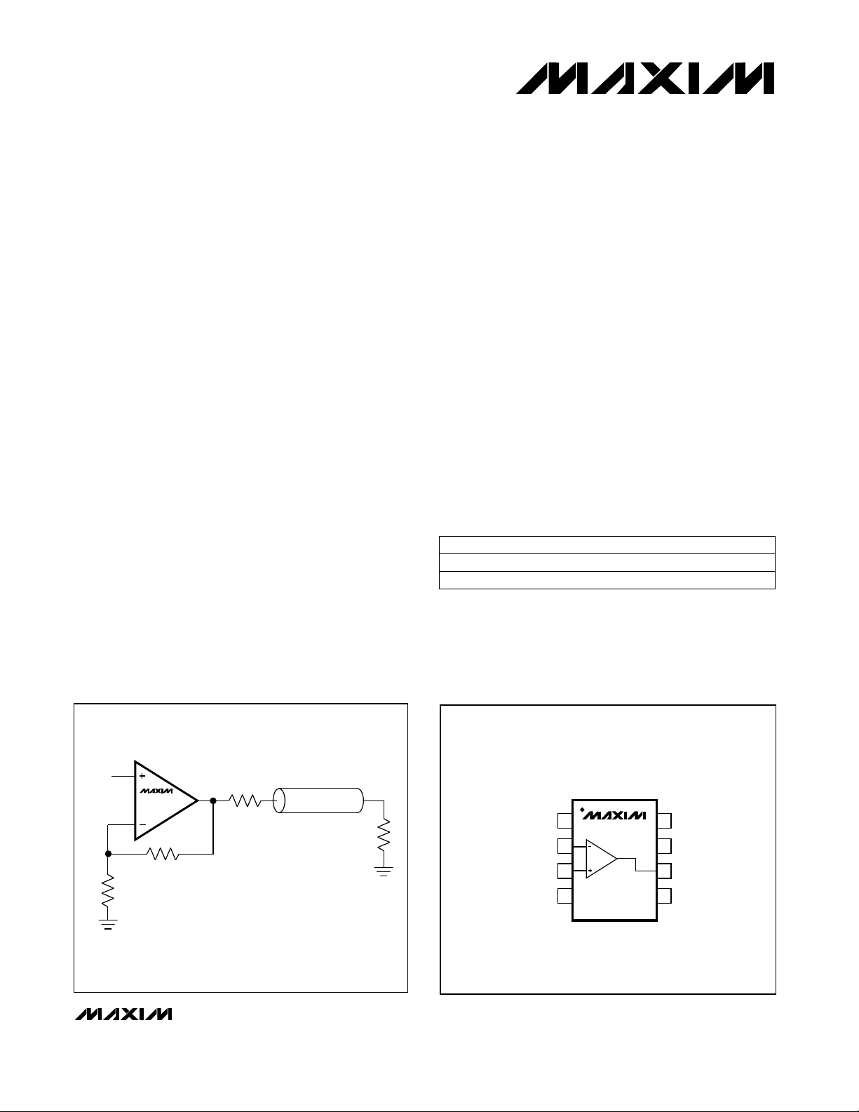
________Typical Application Circuit
INPUT
390Ω
MAX4102
MAX4103
390Ω
75Ω
75Ω
__________________Pin Configuration
TOP VIEW
N.C.
IN+
V
1
MAX4102
MAX4103
2
IN-
3
4
EE
SO
8
N.C.
V
7
CC
OUT
6
N.C.
5
VIDEO CABLE DRIVER
________________________________________________________________
Maxim Integrated Products
1
For free samples & the latest literature: http://www.maxim-ic.com, or phone 1-800-998-8800
Page 2
250MHz, Broadcast-Quality, Low-Power
Video Op Amps
ABSOLUTE MAXIMUM RATINGS
Supply Voltage (VCCto VEE)..................................................12V
Voltage on Any Pin to Ground or Any Other Pin.........V
Short-Circuit Duration (V
Continuous Power Dissipation (T
SO (derate 5.88mW/°C above +70°C).........................471mW
Stresses beyond those listed under “Absolute Maximum Ratings” may cause permanent damage to the device. These are stress ratings only, and functional
operation of the device at these or any other conditions beyond those indicated in the operational sections of the specifications is not implied. Exposure to
absolute maximum rating conditions for extended periods may affect device reliability.
to GND)........................Continuous
OUT
= +70°C)
A
CC
to V
EE
DC ELECTRICAL CHARACTERISTICS
(VCC= 5V, VEE= -5V, TA= T
DC SPECIFICATIONS
Input Offset Voltage
Input Offset Voltage Drift
Input Bias Current
MAX4102/MAX4103
Input Offset Current
Common-Mode Input Resistance
Common-Mode Input Capacitance
Input Voltage Noise
Integrated Voltage Noise
Input Current Noise
Integrated Current Noise
Common-Mode Input Voltage
Open-Loop Voltage Gain
Quiescent Supply Current
Output Voltage Swing
Short-Circuit Output Current
MIN
to T
, unless otherwise noted. Typical values are at TA= +25°C.)
MAX
V
OS
OS
B
OS
INCM
INCM
e
n
i
n
CM
A
VOL
SY
V
OUT
SC
= 0V
OUT
V
= 0V
OUT
V
= 0V, V
OUT
V
OUT
Either input
Either input
f = 100kHz
f = 1MHz to 100MHz
f = 100kHz
f = 1MHz to 100MHz
VS= ±4.5V to ±5.5V
V
OUT
VIN= 0V
RL= ∞
RL = 100Ω
RL = 30Ω, TA= 0°C to +85°C
Short to ground or either supply voltage
IN
= 0V, V
IN
= ±2.0V, VCM= 0V
Operating Temperature Range
MAX4102ESA/MAX4103ESA...........................-40°C to +85°C
Storage Temperature Range.............................-65°C to +160°C
Lead Temperature (soldering, 10sec).............................+300°C
CONDITIONS
= -V
OS
= -V
OS
MAX4102
MAX4103
MAX4102
MAX4103
MAX4102
MAX4103
MAX4102
MAX4103
RL = ∞
RL = 100Ω
66 96
70 100
±3.3 ±3.7
±3.1 ±3.4
7
5
88
63
1.0
1.0
12.5
12.5
UNITSMIN TYP MAXSYMBOLPARAMETER
µV/°C5TCV
nV/√Hz
µV
pA/√Hz
nA
mV0.5 8V
µA39I
µA0.04 0.5I
MΩ5R
pF1C
RMS
RMS
V-2.5 2.5V
dB75 100CMRCommon-Mode Rejection VCM= ±2.5V
dB70 100PSRPower-Supply Rejection
dB
mA4.6 6I
V
mA65 80Output Current
mA90I
2 _______________________________________________________________________________________
Page 3
250MHz, Broadcast-Quality, Low-Power
Video Op Amps
AC ELECTRICAL CHARACTERISTICS
(VCC= 5V, VEE= -5V, RL= 100Ω, A
AC SPECIFICATIONS
0.1dB Bandwidth
Settling Time
Rise/Fall Times tR, t
Differential Gain
Differential Phase DP
Input Capacitance C
Output Resistance R
Spurious-Free Dynamic Range SFDR
= +1 (MAX4102), A
VCL
SYMBOL UNITSCONDITIONS
V
BW-3dB Bandwidth
OUT
≤ 0.1V
MAX4102
MAX4103
OUT
-1V ≤ V
t
DG
s
F
OUT
10% to 90%, -2V ≤ V
10% to 90%, -50mV ≤ V
f = 3.58MHz,
RL= 150Ω
f = 3.58MHz,
RL= 150Ω
IN
f = 10MHz
OUT
fC= 5MHz,
V
= 2V
OUT
= +2 (MAX4103), TA= +25°C, unless otherwise noted.)
VCL
MIN TYP MAXPARAMETER
RMS
MAX4102
MAX4103
250
180
130
80
≤ 2V
≤ 1V ns
≤ 2V 13
OUT
≤ 50mV 1.5
OUT
to 0.1%
to 0.01%
MAX4102
MAX4103
MAX4102
MAX4103
18
30
0.002
0.008
0.002
0.003
degrees
2 pF
MAX4102
0.7
MAX4103 0.7
-78
-76
p-p
MAX4102
MAX4103
MAX4102/MAX4103
MHz
MHz
V/µsSRSlew Rate 350-2V ≤ V
ns
%
Ω
dBc
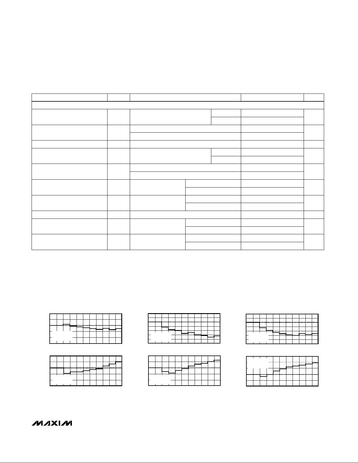
__________________________________________Typical Operating Characteristics
(VCC= 5V, VEE= -5V, RL= 100Ω, TA = +25°C, unless otherwise noted.)
= 2V/V
= 2V/V
MAX4103
IRE
IRE
100
0.004
0.002
0.000
MAX4102/03-02
-0.002
-0.004
-0.006
DIFF GAIN (%)
-0.008
-0.010
0.015
0.010
0.005
0.000
-0.005
DIFF PHASE (deg)
-0.010
DIFFERENTIAL GAIN AND PHASE
MAX4102
RL = 75Ω
= 1V/V
A
VCL
0
RL = 75Ω
= 1V/V
A
VCL
0 100
IRE
IRE
100
DIFFERENTIAL GAIN AND PHASE
MAX4102
0.004
0.002
0.000
-0.002
RL = 150Ω
DIFF GAIN (%)
-0.004
-0.006
0.004
0.002
0.000
-0.002
-0.004
DIFF PHASE (deg)
-0.006
= 1V/V
A
VCL
0
RL = 150Ω
= 1V/V
A
VCL
0 100
IRE
IRE
_______________________________________________________________________________________ 3
100
0.004
0.002
0.000
MAX4102/03-01
-0.002
-0.004
-0.006
DIFF GAIN (%)
-0.008
-0.010
0.004
0.002
0.000
-0.002
-0.004
DIFF PHASE (deg)
-0.006
DIFFERENTIAL GAIN AND PHASE
RL = 150Ω
A
VCL
0
RL = 150Ω
A
VCL
0 100
MAX4102/03-03
Page 4
250MHz, Broadcast-Quality, Low-Power
Video Op Amps
____________________________Typical Operating Characteristics (continued)
(VCC= 5V, VEE= -5V, RL= 100Ω, TA = +25°C, unless otherwise noted.)
DIFFERENTIAL GAIN AND PHASE
MAX4103
0.005
0.000
-0.005
-0.010
RL = 75Ω
DIFF GAIN (%)
-0.015
-0.020
0.020
0.015
0.010
0.005
0.000
-0.005
DIFF PHASE (deg)
-0.010
MAX4102/MAX4103
= 2V/V
A
VCL
0
RL = 75Ω
= 2V/V
A
VCL
0 100
IRE
IRE
100
MAX4102/03-04
-1
GAIN (dB)
-3
-5
MAX4102/MAX4103
OPEN-LOOP GAIN
200
100
0
GAIN (dB)
-100
-200
AND PHASE vs. FREQUENCY
MAX4102/03-07
200
100
0
-100
-200
PHASE (degrees)
VOLTAGE (25mv/div)
SMALL-SIGNAL GAIN vs. FREQUENCY
MAX4102
(A
= +1)
4
3
2
1
0
-2
-4
-6
0.1M 10M1M 100M 1G
VCL
FREQUENCY (Hz)
MAX4102
SMALL-SIGNAL
PULSE RESPONSE (A
VCL
= +1)
IN
OUT
MAX4102/03-09
MAX4102/03-05
GAIN (dB)
GND
GND
SMALL-SIGNAL GAIN vs. FREQUENCY
MAX4103
(A
= +2)
4
3
2
1
0
-1
-2
-3
-4
-5
-6
0.1M 10M1M 100M 1G
VCL
FREQUENCY (Hz)
MAX4102
SMALL-SIGNAL
PULSE RESPONSE (A
VCL
= +5)
IN
VOLTAGE (25mv/div)
OUT
MAX4102/03-06
MAX4102/03-10
GND
GND
= +1)
MAX4102/03-11
-300
VOLTAGE (500mv/div)
GND
TIME (10ns/div)
MAX4102
LARGE-SIGNAL
PULSE RESPONSE (A
IN GND
OUT
TIME (20ns/div)
= +5)
VCL
MAX4102/03-12
GND
VOLTAGE (25mv/div)
TIME (20ns/div)
SMALL-SIGNAL
PULSE RESPONSE (A
IN GND
OUT
-300
1 10k100 1M 100M 1G
FREQUENCY (Hz)
MAX4102
LARGE-SIGNAL
PULSE RESPONSE (A
VCL
IN GND
VOLTAGE (500mv/div)
OUT
TIME (10ns/div)
4 _______________________________________________________________________________________
MAX4103
TIME (10ns/div)
VCL
= +2)
MAX4102/03-13
GND
Page 5

250MHz, Broadcast-Quality, Low-Power
Video Op Amps
____________________________Typical Operating Characteristics (continued)
(VCC= 5V, VEE= -5V, RL= 100Ω, TA = +25°C, unless otherwise noted.)
MAX4103
SMALL-SIGNAL
PULSE RESPONSE (A
VCL
= +10)
IN GND
VOLTAGE (25mv/div)
OUT
TIME (20ns/div)
MAX4102
DISTORTION vs. FREQUENCY
(A
= +1)
-40
V
= 2Vp-p
OUT
= 100Ω
R
-50
L
-60
-70
-80
-90
HARMONIC DISTORTION (dBc)
-100
-110
2ND HARMONIC
0.1 1 10 100
VCL
3RD HARMONIC
FREQUENCY (MHz)
MAX4103
DISTORTION vs. FREQUENCY
(A
= +5)
-40
V
= 2Vp-p
OUT
= 100Ω
R
-50
L
-60
2ND HARMONIC
-70
-80
-90
HARMONIC DISTORTION (dBc)
-100
-110
0.1 1 10 100
VCL
3RD HARMONIC
FREQUENCY (MHz)
MAX4102/03-14
IN GND
GND
VOLTAGE (500mv/div)
OUT
1
V
OUT
= 100Ω
MAX4102/03-17
MAX4102/03-20
R
L
A
VCL
0.1
0.01
TOTAL HARMONIC DISTORTION (%)
0.001
0.1 1 10 100
1
V
OUT
= 100Ω
R
L
A
VCL
0.1
0.01
TOTAL HARMONIC DISTORTION (%)
0.001
0.1 1 10 100
MAX4103
LARGE-SIGNAL
PULSE RESPONSE (A
TIME (10ns/div)
= +2)
VCL
MAX4102/03-15
MAX4102
TOTAL HARMONIC DISTORTION
vs. FREQUENCY
= 2Vp-p
= +1
FREQUENCY (MHz)
MAX4103
TOTAL HARMONIC DISTORTION
vs. FREQUENCY
= 2Vp-p
= +2
FREQUENCY (MHz)
PULSE RESPONSE (A
IN GND
GND
VOLTAGE (500mv/div)
OUT
DISTORTION vs. FREQUENCY
-40
V
OUT
= 100Ω
R
-50
MAX4102/03-18
HARMONIC DISTORTION (dBc)
-100
-110
MAX4102/03-21
HARMONIC DISTORTION (dBc)
-100
L
-60
-70
-80
-90
0.1 1 10 100
-40
f
OUT
V
-50
-60
-70
-80
-90
OUT
A
VCL
10 100 1k
= 2Vp-p
2ND HARMONIC
5MHz DISTORTION vs. LOAD
LARGE-SIGNAL
TIME (20ns/div)
MAX4103
(A
FREQUENCY (MHz)
MAX4102
= 5MHz
= 2Vp-p
= +1
3RD HARMONIC
MAX4103
VCL
= +2)
VCL
3RD HARMONIC
2ND HARMONIC
LOAD (Ω)
= +10)
MAX4102/MAX4103
MAX4102/03-16
GND
MAX4102/03-19
MAX4102/03-22
_______________________________________________________________________________________
5
Page 6

250MHz, Broadcast-Quality, Low-Power
Video Op Amps
____________________________Typical Operating Characteristics (continued)
(VCC= 5V, VEE= -5V, RL= 100Ω, TA = +25°C, unless otherwise noted.)
MAX4103
5MHz DISTORTION vs. LOAD
-40
f
= 5MHz
OUT
= 2Vp-p
V
-50
-60
-70
-80
HARMONIC DISTORTION (dBc)
-90
-100
MAX4102/MAX4103
OUT
= +2
A
VCL
10 100 1k
2ND HARMONIC
3RD HARMONIC
LOAD (Ω)
-40
MAX4102/03-23
-50
-60
-70
-80
HARMONIC DISTORTION (dBc)
-90
-100
INPUT VOLTAGE NOISE
vs. FREQUENCY
100
MAX4102/03-26
MAX4102
10
NOISE (pA/√Hz)
VOLTAGE NOISE (nV/√Hz)
1
1
MAX4103
1k
FREQUENCY (Hz)
10k10 100 100k
5MHz DISTORTION vs. OUTPUT SWING
MAX4102
f
= 5MHz
OUT
= 100Ω
R
L
= +1
A
VCL
2ND HARMONIC
3RD HARMONIC
110
OUTPUT SWING (Vp-p)
MAX4102/03-24
-50
-60
-70
-80
HARMONIC DISTORTION (dBc)
-90
-100
INPUT CURRENT NOISE
vs. FREQUENCY
10
5
1
1
FREQUENCY (Hz)
1k
10k10 100 100k
100
MAX4102/03-27
POWER-SUPPLY REJECTION (dB)
5MHz DISTORTION vs. OUTPUT SWING
MAX4103
-40
f
= 5MHz
OUT
= 100Ω
R
L
= +2
A
VCL
2ND HARMONIC
3RD HARMONIC
110
OUTPUT SWING (Vp-p)
MAX4102/03-25
POWER-SUPPLY
REJECTION vs. FREQUENCY
90
80
70
60
50
40
30
20
10
0
0.2M 10M 100M1M 1G
FREQUENCY (Hz)
MAX4102/03-28
100
COMMON-MODE REJECTION
90
80
70
60
50
40
30
20
COMMON-MODE REJECTION (dB)
10
0
0.03M 0.1M 1M 10M 100M 1G
MAX4103
MAX4102
FREQUENCY (Hz)
MAX4102/03-29
OUTPUT RESISTANCE
vs. FREQUENCY
26.0
22.8
19.7
16.5
13.3
10.2
7.0
3.9
OUTPUT IMPEDANCE (Ω)
0.7
0.4
0
0.1M 10M 100M1M 1G
FREQUENCY (Hz)
0.65
0.60
MAX4102/03-30
0.55
0.50
0.45
VOLTAGE (mV)
0.40
0.35
0.30
INPUT OFFSET VOLTAGE
vs. TEMPERATURE
-75 -50 -25 50 75 125
0 25 100
TEMPERATURE (°C)
6 _______________________________________________________________________________________
MAX4102/03-31
Page 7

250MHz, Broadcast-Quality, Low-Power
Video Op Amps
____________________________Typical Operating Characteristics (continued)
(VCC= 5V, VEE= -5V, RL= 100Ω, TA = +25°C, unless otherwise noted.)
INPUT OFFSET CURRENT
vs. TEMPERATURE
0.055
0.050
0.045
0.040
0.035
CURRENT (µA)
0.030
0.025
0.020
-75 -50 -25 50 75 125
0 25 100
TEMPERATURE (°C)
NEGATIVE OUTPUT SWING
vs. TEMPERATURE
-3.2
-3.3
-3.4
-3.5
RL = 100Ω
4.0
3.5
MAX4102/03-32
3.0
2.5
2.0
1.5
OUTPUT SWING (Vp-p)
1.0
0.5
0
10 30 50 110 150
6
MAX4102/03-35
5
OUTPUT SWING
vs. LOAD RESISTANCE
70 90 130
LOAD RESISTANCE (Ω)
POWER-SUPPLY CURRENT
vs. TEMPERATURE
3.9
3.8
MAX4102/03-33
3.7
3.6
3.5
3.4
OUTPUT SWING (Vp-p)
3.3
3.2
8
7
MAX4102/03-36
6
5
POSITIVE OUTPUT SWING
vs. TEMPERATURE
RL = ∞
RL = 100Ω
-75 -50 -25 75 125
05025 100
TEMPERATURE (°C)
INPUT BIAS CURRENT
vs. TEMPERATURE
MAX4102/MAX4103
MAX4102/03-34
MAX4102/03-37
-3.6
-3.7
OUTPUT SWING (Vp-p)
-3.8
-3.9
-75 -50 -25 75 125
TEMPERATURE (°C)
RL = ∞
05025 100
_______________________________________________________________________________________
CURRENT (mA)
4
3
-75 -50 -25 75 125
05025 100
TEMPERATURE (°C)
4
CURRENT (µA)
3
2
1
-75 -50 -25 75 125
05025 100
TEMPERATURE (°C)
7
Page 8

250MHz, Broadcast-Quality, Low-Power
Video Op Amps
_____________________Pin Description
FUNCTIONNAMEPIN
Not internally connectedN.C.1
Inverting InputIN-2
Noninverting InputIN+3
4
7
_______________Detailed Description
MAX4102/MAX4103
The MAX4102/MAX4103 low-power, high-speed op
amps feature ultra-low differential gain and phase, and
are optimized for the highest quality video applications.
Differential gain and phase errors are 0.002%/0.002°
for the MAX4102 and 0.008%/0.003° for the MAX4103.
The MAX4102 also features a -3dB bandwidth of over
250MHz and 0.1dB gain-flatness of 130MHz. The
MAX4103 features a -3dB bandwidth of 180MHz and a
0.1dB bandwidth of 80MHz.
The MAX4102 is unity-gain stable, and the MAX4103 is
optimized for closed-loop gains of 2V/V (6dB) and higher.
Both devices drive back-terminated 50Ω or 75Ω cables to
±3.1V (min) and deliver an output current of 80mA.
Available in a small 8-pin SO package, the MAX4102/
MAX4103 are ideal for high-definition TV systems (in
RGB, broadcast, or consumer video applications) that
benefit from low power consumption and superior differential gain and phase characteristics.
V
EE
V
CC
Negative Power Supply. Connect
to -5V
Not internally connectedN.C.5
Amplifier OutputOUT6
Positive Power Supply. Connect
to +5V
Not internally connectedN.C.8
__________Applications Information
Grounding, Bypassing,
and PC Board Layout
In order to achieve the full bandwidth, Microstrip and
Stripline techniques are recommended in most cases.
To ensure your PC board does not degrade the amp’s
performance, it’s wise to design the board for a frequency greater than 1GHz. Even with very short runs,
it’s good practice to use this technique at critical
points, such as inputs and outputs. Whether you use a
constant-impedance board or not, observe the following guidelines when designing the board:
• Do not use wire-wrap boards, because they are too
inductive.
• Do not use IC sockets. They increase parasitic
capacitance and inductance.
• In general, surface-mount components have shorter
leads and lower parasitic reactance, and give better
high-frequency performance than through-hole components.
• The PC board should have at least two layers, with
one side a signal layer and the other a ground plane.
• Keep signal lines as short and as straight as possible. Do not make 90° turns; round all corners.
• The ground plane should be as free from voids as
possible.
On Maxim’s evaluation kit, the ground plane has been
removed from areas where keeping the trace capacitance to a minimum is more important than maintaining
ground continuity. For example, the ground plane has
been removed from beneath the IC to minimize pin
capacitance.
The bypass capacitors should include a 0.1µF at each
supply pin and the ground plane, located as close to the
package as possible. Then place a 10µF to 15µF lowESR tantalum at the point of entry (to the PC board) of
the power-supply pins. The power-supply trace should
lead directly from the tantalum capacitor to the V
V
pins to maintain the low differential gain and phase
EE
of these devices.
CC
and
Setting Gain
The MAX4102/MAX4103 are voltage-feedback op
amps that can be configured as an inverting or noninverting gain block, as shown in Figures 1a and 1b. The
gain is determined by the ratio of two resistors and
does not affect amplifier frequency compensation.
In the unity-gain configuration (Figure 1c), maximum
bandwidth and stability are achieved with the MAX4102
when a small feedback resistor is included. This resistor suppresses the negative effects of parasitic inductance and capacitance. A value of 24Ω provides the
best combination of wide bandwidth, low peaking, and
fast settling time. In addition, this resistor reduces the
errors from input bias currents.
Choosing Resistor Values
The values of feedback and input resistors used in the
inverting or noninverting gain configurations are not
critical (as is the case with current-feedback amplifiers), but should be kept small and noninductive.
8 _______________________________________________________________________________________
Page 9

250MHz, Broadcast-Quality, Low-Power
Video Op Amps
The input capacitance of the MAX4102/MAX4103 is
approximately 2pF. In either the inverting or noninverting configuration, the bandwidth limit caused by the
package capacitance and resistor time constant is
f
= 1 / (2Π RC), where R is the parallel combination
3dB
of the input and feedback resistors (RFand RGin
Figure 2) and C is the package and board capacitance
at the inverting input. RS1and RS2represent the input
termination resistors. Table 1 shows the typical bandwidth and resistor values for several gain configurations.
MAX4100
MAX4102
MAX4101
MAX4103
MAX4100
MAX4102
MAX4101
MAX4103
T
R
F
V
OUT
R
F
V
OUT
R
G
R
T
IN
V
= -(RF / RG)V
OUT
V
IN
Figure 1a. Inverting Gain Configuration
R
G
V
IN
V
= [1 + (RF / RG)]V
OUT
IN
R
Table 1. Resistor and Bandwidth Values
for Various Gain Configurations
DEVICE
MAX4102 ∞ 24 250
MAX4102 200 200 100
MAX4103 200 200 180
MAX4103 50 200 40
MAX4103 30 270 20
MAX4103 200 200 180
MAX4103 75 150 140
MAX4103 50 250 75
GAIN
(V/V)
1
2
2
5
10
-1
-2
-5
R
(Ω)
R
G
(Ω)
R
F
(Ω)
50
50
50
50
50
56
150
∞
MAX4103 50 500 35∞-10
Note: Refer to Figure 1a for inverting gain configurations and
Figure 1b for noninverting gain configurations. R
for 50Ω systems.
Resistor Types
Surface-mount resistors are the best choice for highfrequency circuits. They are of similar material to the
metal-film resistors, but are deposited using a thick-film
process in a flat, linear manner so that inductance is
minimized. Their small size and lack of leads also minimize parasitic inductance and capacitance, thereby
yielding more predictable performance.
R
V
IN
G
R
F
T
is calculated
T
BANDWIDTH
(MHz)
MAX4102/MAX4103
Figure 1b. Noninverting Gain Configuration
24Ω
MAX4100
MAX4102
MAX4101
MAX4103
V
IN
V
= V
OUT
IN
V
Figure 1c. MAX4102 Unity-Gain Buffer Configuration
_______________________________________________________________________________________ 9
OUT
R
S1
C
R
S2
MAX4100
MAX4102
MAX4101
MAX4103
V
OUT
Figure 2. Effect of Feedback Resistor Values and Parasitic
Capacitance on Bandwidth
Page 10

250MHz, Broadcast-Quality, Low-Power
Video Op Amps
Driving Capacitive Loads
When driving 50Ω or 75Ω back-terminated transmission
lines, capacitive loading is not an issue. The MAX4102/
MAX4103 can typically drive 5pF and 20pF, respectively.
Figure 3a illustrates how a capacitive load influences the
amplifier’s peaking without an isolation resistor (RS).
Figure 3b shows how an isolation resistor decreases the
amplifier’s peaking. By using a small isolation resistor
6
A
= +1
VCL
5
4
3
2
MAX4102/MAX4103
1
GAIN (dB)
0
-1
-2
-3
-4
0.1M 10M1M 100M 1G
CL = 15pF
CL = 10pF
CL = 5pF
FREQUENCY (Hz)
between the amplifier output and the load, large capacitance values may be driven without oscillation (Figure
4a). In most cases, less than 50Ωis sufficient. Use Figure
4b to determine the value needed in your application.
Determine the worst-case maximum capacitive load you
may encounter and select the appropriate resistor from
the graph.
4
CL = 10pF
3
2
1
0
-1
GAIN (dB)
-2
-3
-4
-5
-6
0.1M 10M1M 100M 1G
RS = 22Ω
RS = 33Ω
FREQUENCY (Hz)
RS = 10Ω
Figure 3a. MAX4102 Bandwidth vs. Capacitive Load
24Ω
))
S
R
S
C
L
R
L
(No Isolation Resistor (R
MAX4102
V
IN
Figure 4a. Using an Isolation Resistor (RS) for Large Capacitive
Figure 3b. MAX4102 Bandwidth vs. 10pF Capacitive Load and
Isolation Resistor
40
35
30
25
20
15
ISOLATION RESISTANCE (Ω)
10
5
0 100 150 200
MAX4102
MAX4103
50 250
CAPACITIVE LOAD (pF)
Figure 4b. Isolation vs. Capacitive Load
Loads (MAX4102)
10 ______________________________________________________________________________________
Page 11

250MHz, Broadcast-Quality, Low-Power
Video Op Amps
________________________________________________________Package Information
DIM
D
A
0.101mm
e
A1
B
0.004in.
C
L
0°-8°
Narrow SO
HE
SMALL-OUTLINE
PACKAGE
(0.150 in.)
A
A1
B
C
E
H
DIM
D
D
D
INCHES MILLIMETERS
MIN
0.053
0.004
0.014
0.007
0.150
e
0.228
L
0.016
PINS
8
14
16
MAX
0.069
0.010
0.019
0.010
0.157
0.244
0.050
INCHES MILLIMETERS
MIN
MAX
0.189
0.197
0.337
0.344
0.386
0.394
MIN
1.35
0.10
0.35
0.19
3.80
5.80
0.40
MIN
4.80
8.55
9.80
1.270.050
MAX
1.75
0.25
0.49
0.25
4.00
6.20
1.27
MAX
5.00
8.75
10.00
21-0041A
MAX4102/MAX4103
___________________Chip Information
TRANSISTOR COUNT: 51
SUBSTRATE CONNECTED TO: V
______________________________________________________________________________________ 11
EE
Page 12

250MHz, Broadcast-Quality, Low-Power
Video Op Amps
MAX4102/MAX4103
Maxim cannot assume responsibility for use of any circuitry other than circuitry entirely embodied in a Maxim product. No circuit patent licenses are
Maxim cannot assume responsibility for use of any circuitry other than circuitry entirely embodied in a Maxim product. No circuit patent licenses are
Maxim cannot assume responsibility for use of any circuitry other than circuitry entirely embodied in a Maxim product. No circuit patent licenses are
Maxim cannot assume responsibility for use of any circuitry other than circuitry entirely embodied in a Maxim product. No circuit patent licenses are
implied. Maxim reserves the right to change the circuitry and specifications without notice at any time.
implied. Maxim reserves the right to change the circuitry and specifications without notice at any time.
implied. Maxim reserves the right to change the circuitry and specifications without notice at any time.
implied. Maxim reserves the right to change the circuitry and specifications without notice at any time.
12
__________________Maxim Integrated Products, 120 San Gabriel Drive, Sunnyvale, CA 94086 (408) 737-7600
12
__________________Maxim Integrated Products, 120 San Gabriel Drive, Sunnyvale, CA 94086 (408) 737-7600
12
__________________Maxim Integrated Products, 120 San Gabriel Drive, Sunnyvale, CA 94086 (408) 737-7600
12
__________________Maxim Integrated Products, 120 San Gabriel Drive, Sunnyvale, CA 94086 (408) 737-7600
© 1996 Maxim Integrated Products Printed USA is a registered trademark of Maxim Integrated Products.
© 1996 Maxim Integrated Products Printed USA is a registered trademark of Maxim Integrated Products.
© 1996 Maxim Integrated Products Printed USA is a registered trademark of Maxim Integrated Products.
© 1996 Maxim Integrated Products Printed USA is a registered trademark of Maxim Integrated Products.
 Loading...