

Page 1
AVAILABLE
For pricing, delivery, and
ordering information, please contact Maxim Direct
at 1-888-629-4642, or visit Maxim’s website at www.maximintegrated.com.
General Description
The MAX4069–MAX4072 low-cost, bidirectional, highside, current-sense amplifiers are ideal for monitoring
battery charge and discharge currents in notebooks,
cell phones, and other portable equipment. They feature up to 24V input common-mode voltage range, low
100µA supply current (which drops to only 10µA in
shutdown), and a total output error of less than 1.5%.
The wide 1.35V to 24V input common-mode range is
independent of the supply voltage, ensuring that the
current-sense feedback remains accurate even when
connected to a battery pack in deep discharge.
To achieve maximum flexibility, an external current-sense
resistor is used along with a Gain Select pin to choose
either 50V/V or 100V/V. A single output pin continuously
monitors the transition from charge to discharge and
avoids the need for a separate polarity output. The
MAX4070 contains an internal 2.5V reference. The
charging current is represented by an output voltage
from 2.5V to V
CC
, while discharge current is given from
2.5V to GND. The MAX4071 is similar, but with a reference voltage of 1.5V. The MAX4069 has an adjustable
reference voltage, set by two external resistors. The
MAX4072 has an input for an external reference.
The MAX4069/MAX4071/MAX4072 operate from a 2.7V to
24V single supply. The MAX4070 operates from a 3.6V to
24V single supply. All devices are specified over the
automotive operating temperature range, -40°C to
+125°C. The MAX4070/MAX4071/MAX4072 are available
in 8-pin µMAX and 8-pin thin QFN packages. The
MAX4069 is available in a 10-pin µMAX
®
package.
Applications
Notebook Fuel Gauging
Smart-Battery Packs/Chargers
Motor Control
Power-Management Systems
Cell-Phone Battery-Current Monitoring
Features
♦ Bidirectional, Compact, Current-Sense Solution
♦ Total Output Error Less than 1.5%
♦ Selectable Gain of 50V/V or 100V/V
♦ Wide 1.35V to 24V Common-Mode Range
Independent of Supply Voltage
♦ 2.7V to 24V Single-Supply Operation
♦ Internal Precision Reference
Adjustable (MAX4069)
2.50V (MAX4070)
1.50V (MAX4071)
♦ Low 100µA Supply Current
♦ 10µA Supply Current in Shutdown
♦ Available in Space-Saving Packages
8-Pin Thin QFN (MAX4070/MAX4071/MAX4072)
8-Pin µMAX (MAX4070/MAX4071MAX4072)
10-Pin µMAX (MAX4069)
Bidirectional, High-Side, Current-Sense
Amplifiers with Reference
Ordering Information
MAX4070
V
BATT
= 1.35V TO 24V
VCC = 3.6V TO 24V
FROM BATTERY
CHARGER
R
SENSE
LOAD
TO ADC
2.5V
V
CC
GSEL
GND
RS- RS+
REFOUT
OUT
SHDN
Typical Operating Circuit
Pin Configurations and Selector Guide appear at end of
data sheet.
*
EP = Exposed pad.
µMAX is a registered trademark of Maxim Integrated Products, Inc.
19-2423; Rev 3; 11/08
MAX4069–MAX4072
PART TEMP RANGE PIN-PACKAGE
MAX4069AUB -40°C to +125°C 10 µMAX —
MAX4070AUA -40°C to +125°C 8 µMAX —
MAX4070ATA -40°C to +125°C 8 Thin QFN-EP* ABN
MAX4071AUA -40°C to +125°C 8 µMAX —
MAX4071ATA -40°C to +125°C 8 Thin QFN-EP* ABO
MAX4072AUA -40°C to +125°C 8 µMAX —
MAX4072ATA -40°C to +125°C 8 Thin QFN-EP* ABP
TOP
MARK
Page 2
Bidirectional, High-Side, Current-Sense
Amplifiers with Reference
ABSOLUTE MAXIMUM RATINGS
ELECTRICAL CHARACTERISTICS
(V
RS
+
= V
RS
-
= V
CC
= 2.7V to 24V, V
SENSE
= V
RS
+
- V
RS
-
= 0V, I
REFOUT
= 0, V
SHDN
= VCC, V
GSEL
= GND, V
REFIN
= 2.5V (MAX4072),
T
A
= T
MIN
to T
MAX
, unless otherwise noted. Typical values are at TA= +25°C and at VCC= V
RS
+
= 12V.) (Notes 1, 2)
Stresses beyond those listed under “Absolute Maximum Ratings” may cause permanent damage to the device. These are stress ratings only, and functional
operation of the device at these or any other conditions beyond those indicated in the operational sections of the specifications is not implied. Exposure to
absolute maximum rating conditions for extended periods may affect device reliability.
VCC, RS+, RS- to GND ...........................................-0.3V to +26V
OUT to GND....................-0.3V to Lesser of (V
CC
+ 0.3V) or 15V
Differential Input Voltage (V
RS
+
- V
RS
-
) ..............................±0.3V
GSEL, SHDN, REFOUT, REFIN
and ADJ to GND.....................................-0.3V to (V
CC
+ 0.3V)
OUT Short-Circuit Duration to GND
or to Lesser of (V
CC
or 15V)...................................Continuous
REFOUT Short Circuit to V
CC
or GND........................Continuous
Current into Any Pin ..........................................................±20mA
Continuous Power Dissipation (T
A
= +70°C)
8-Pin µMAX (derate 4.5 mW/°C above +70°C) ............362mW
8-Pin Thin QFN (derate 24.4mW/°C above +70°C) ...1951mW
10-Pin µMAX (derate 5.6 mW/°C above +70°C) .......444.4mW
Operating Temperature Range .........................-40°C to +125°C
Junction Temperature......................................................+150°C
Storage Temperature Range .............................-65°C to +150°C
Lead Temperature (soldering, 10s) .................................+300°C
MAX4069–MAX4072
2
Maxim Integrated
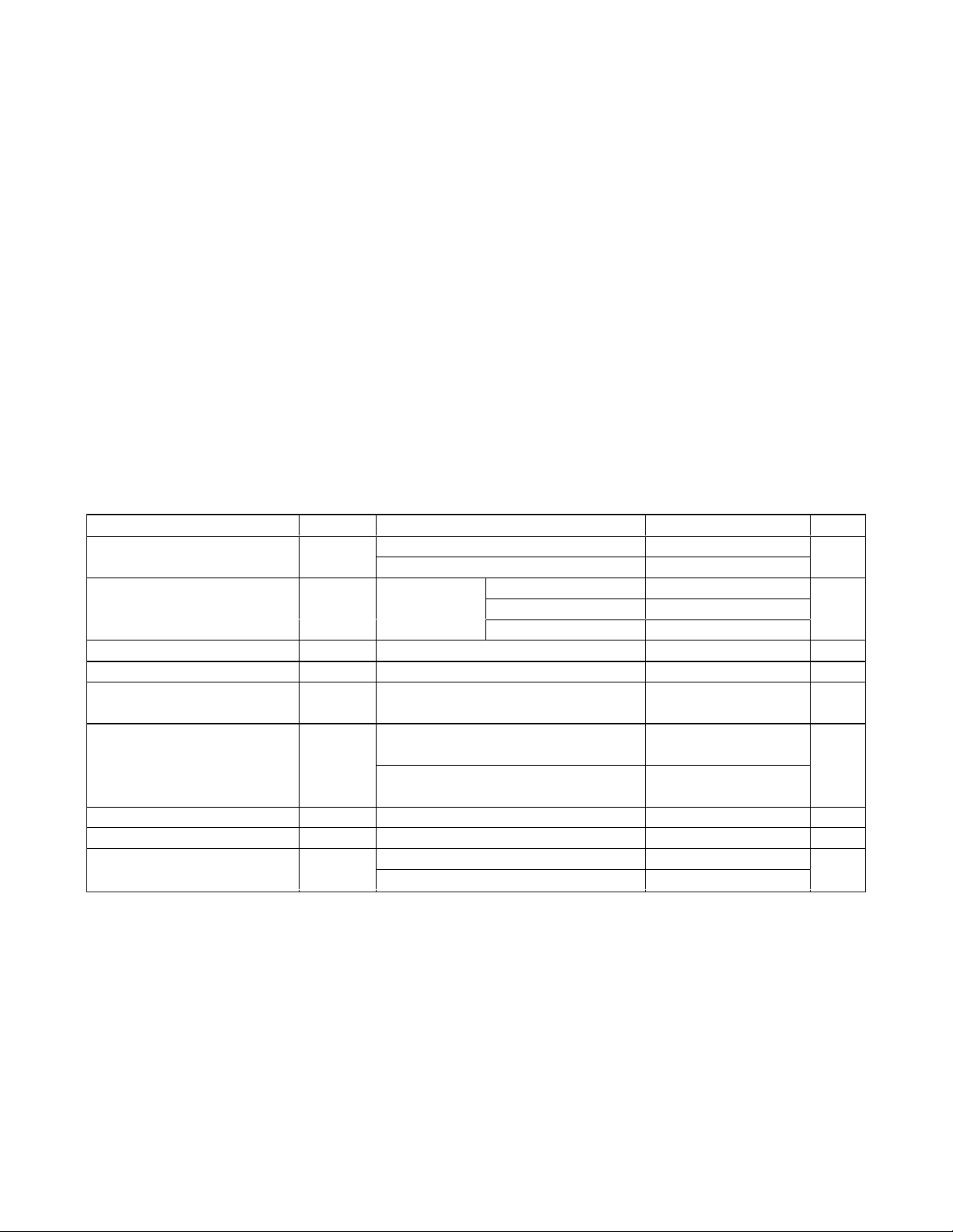
PARAMETER SYMBOL CONDITIONS MIN TYP MAX UNITS
Operating Voltage Range
(Note 3)
Input-Referred Offset Voltage
(Note 5)
V
CC
V
OS
Common-Mode Input Range CMVR Guaranteed by CMRR test 1.35 24 V
Common-Mode Rejection Ratio CMRR 1.35V ≤ V
Supply Current I
Shutdown Supply Current I
CC
CC SHDN
Leakage Current V
Input Bias Current I
Recommended Full-Scale Sense
Voltage (Note 6)
RS+, IRS-
V
SENSE
MAX4069/MAX4071/MAX4072 (Note 4) 2.7 24
MAX4070 3.6 24
V
= V
CC
RS-
CC
A
CC
= V
= T
= V
RS+
= 12V
RS+ = VRS-
RS+
MIN
RS+
to T
V
V
T
V
SHDN = GND, T
V
= V
CC
RS+
SHDN = GND
= V
RS+
RS-
V
= V
CC
RS+
Gain = 50V/V 75
Gain = 100V/V 50
TA = +25°C 0.08 0.25
=
TA = -40°C to +85°C 0.8
T
= T
A
≤ 24V, V
= V
= 24V, RL = open,
RS-
MAX
= V
= 5.5V,
RS-
= +25°C
A
= V
= 24V,
RS-
to T
MIN
MAX
= 12V 100 120 dB
CC
100 250 µA
9
10 30
1
= 24V, VCC = 0V 0.1 0.5 µA
= V
= 24V 0 2.4 5 µA
RS-
V
mV
µA
mV
Page 3
Bidirectional, High-Side, Current-Sense
Amplifiers with Reference
ELECTRICAL CHARACTERISTICS (continued)
(V
RS
+
= V
RS
-
= V
CC
= 2.7V to 24V, V
SENSE
= V
RS
+
- V
RS
-
= 0V, I
REFOUT
= 0, V
SHDN
= VCC, V
GSEL
= GND, V
REFIN
= 2.5V (MAX4072),
T
A
= T
MIN
to T
MAX
, unless otherwise noted. Typical values are at TA= +25°C and at VCC= V
RS
+
= 12V.) (Notes 1, 2)
MAX4069–MAX4072
Maxim Integrated
3
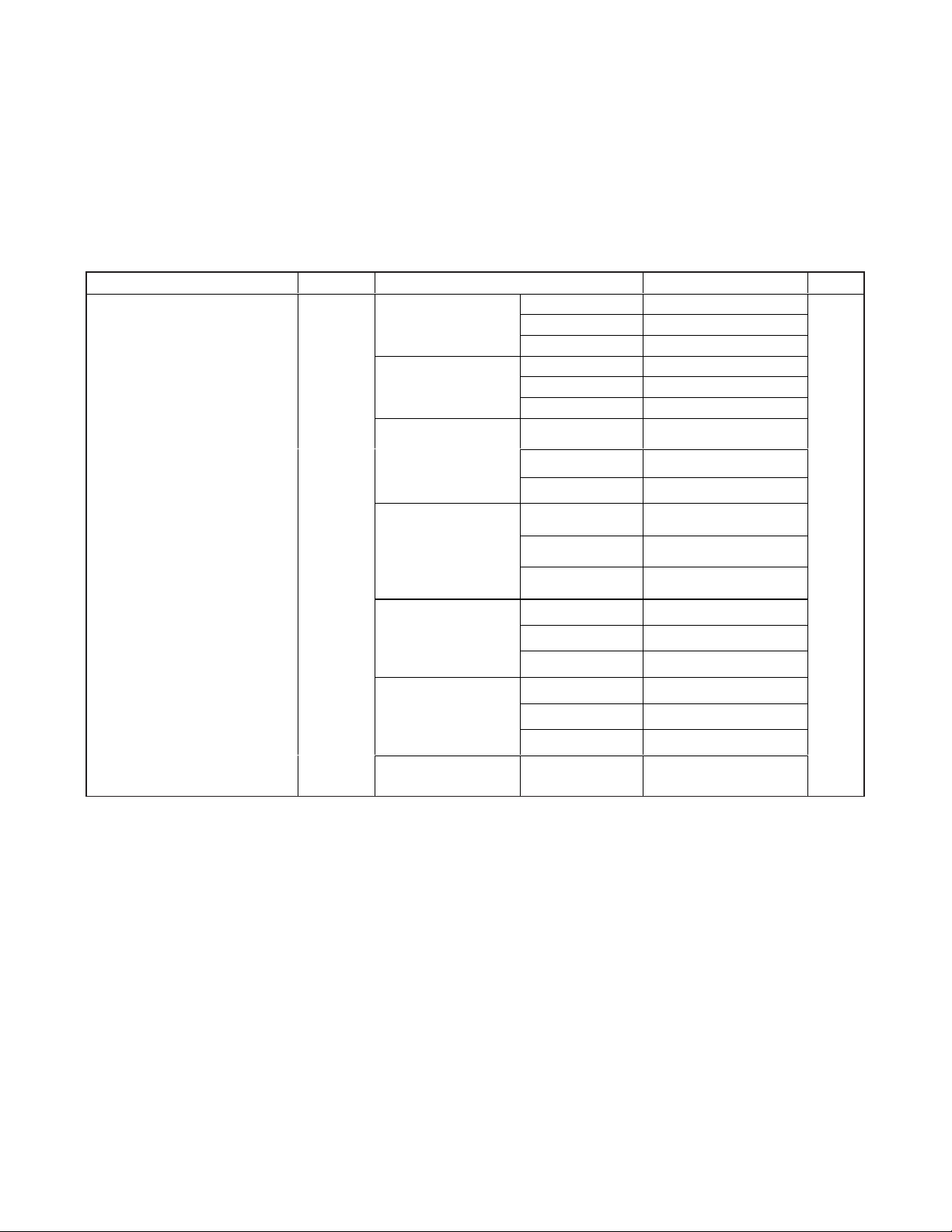
PARAMETER SYMBOL CONDITIONS MIN TYP MAX UNITS
Total OUT Voltage Error (Note 7)
V
SENSE
V
CC
gain = 50
V
SENSE
V
CC
gain = 100
MAX4069/MAX4070/
MAX4072:
V
SENSE
V
CC
gain = 50
MAX4069/MAX4070/
MAX4072:
V
SENSE
V
CC
gain = 100
= V
= V
= V
= V
= 75mV,
= 12V,
RS+
= 50mV,
= 12V,
RS+
= -35mV,
= 12V,
RS+
= -17.5mV,
= 12V,
RS+
TA = +25°C ±0.25 ±1.0
TA = - 40°C to + 85°C ±1.5
T
= T
MIN
to T
MAX
A
TA = +25°C ±0.25 ±1.0
TA = - 40°C to + 85°C ±1.5
T
= T
MIN
to T
MAX
A
TA = +25°C ±0.4 ±1.0
TA = - 40°C to + 85°C ±2.0
TA = T
MIN
to T
MAX
TA = +25°C ±0.8 ±2.0
TA = - 40°C to + 85°C ±4.0
= T
MIN
to T
MAX
T
A
±2.0
±2.5
±3.0
%
±6
MAX4071:
V
= -15mV,
SENSE
= V
V
CC
RS+
gain = 50
MAX4071:
V
= -7.5mV,
SENSE
= V
V
CC
RS+
gain = 100
V
= 3mV,
SENSE
V
= 12V , V
C C
= 12V,
= 12V,
= 12V
RS +
TA = +25°C ±1.0 ±2.5
TA = - 40°C to + 85°C ±4.0
T
= T
MIN
to T
MAX
A
±6.0
TA = +25°C ±2.0 ±5
TA = - 40°C to + 85°C ±10
T
= T
A
T
A
to T
MIN
MAX
= +25°C ±3
±15
Page 4
Bidirectional, High-Side, Current-Sense
Amplifiers with Reference
ELECTRICAL CHARACTERISTICS (continued)
(V
RS
+
= V
RS
-
= V
CC
= 2.7V to 24V, V
SENSE
= V
RS
+
- V
RS
-
= 0V, I
REFOUT
= 0, V
SHDN
= VCC, V
GSEL
= GND, V
REFIN
= 2.5V (MAX4072),
T
A
= T
MIN
to T
MAX
, unless otherwise noted. Typical values are at TA= +25°C and at VCC= V
RS
+
= 12V.) (Notes 1, 2)
MAX4069–MAX4072
4
Maxim Integrated
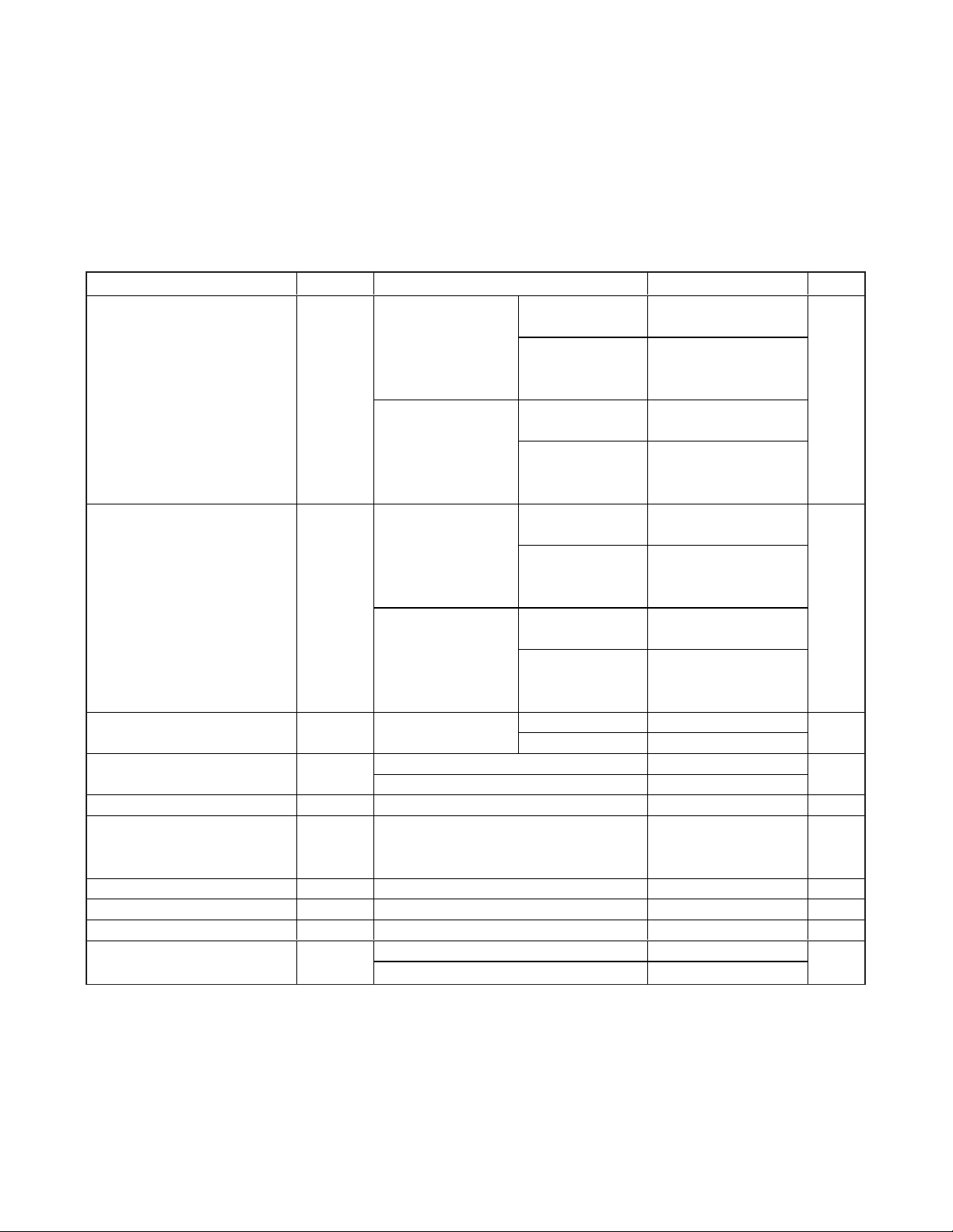
PARAMETER SYMBOL CONDITIONS MIN TYP MAX UNITS
OUT Voltage High V
OUT Voltage Low V
CC
- V
OL
-3dB Bandwidth BW
Gain A
Capacitive-Load Stability 100 pF
Power-Supply Rejection Ratio PSRR
Logic Low Voltage (GSEL, SHDN)VILVCC = 3.6V or 24V 0.6 V
Logic High Voltage (GSEL, SHDN)VIHVCC = 3.6V or 24V 2 V
Gain-Select Input Current I
Shutdown Input Current I
GSEL
SHDN
I
OUT
V
SENSE
V
RS+
I
OUT
V
SENSE
V
RS+
= 10µA,
= 100mV,
= V
= 500µA,
= 100mV,
= V
CC
CC
MAX4071,
V
= 2.7V
CC
MAX4069/MAX4070/
MAX4072,
V
= 3.6V
CC
MAX4071,
= 2.7V
V
CC
MAX4069/MAX4070/
MAX4072,
V
= 3.6V
CC
65 150
65 150
90 250
90 250
MAX4071,
V
= 2.7V
I
= -10µA,
OUT
V
= -100mV,
SENSE
= V
V
RS+
CC
I
= -500µA,
OUT
= -100mV,
V
SENSE
V
= V
RS+
CC
V
= 50mV,
SENSE
V
= 12V, CL = 100pF
CC
CC
MAX4069/MAX4070/
MAX4072,
V
= 3.6V
CC
MAX4071,
= 2.7V
V
CC
100 250
MAX4069/MAX4070/
MAX4072,
V
= 3.6V
CC
100 250
Gain = 50V/V 100
Gain = 100V/V 40
GSEL = GND 50
GSEL = V
V
CC
CC
= 2.7V to 24V
(MAX4069/MAX4071/MAX4072),
V
= 3.6V to 24V (MAX4070)
CC
100 120 dB
100
520
520
V
OH
GSEL = VCC = 24V or GND 0.01 1 µA
SHDN = V
SHDN = GND, V
= 24V 3 12
CC
= 24V 0.01 1
CC
mV
mV
kHz
V/V
µA
Page 5
Bidirectional, High-Side, Current-Sense
Amplifiers with Reference
ELECTRICAL CHARACTERISTICS (continued)
(V
RS
+
= V
RS
-
= V
CC
= 2.7V to 24V, V
SENSE
= V
RS
+
- V
RS
-
= 0V, I
REFOUT
= 0, V
SHDN
= VCC, V
GSEL
= GND, V
REFIN
= 2.5V (MAX4072),
T
A
= T
MIN
to T
MAX
, unless otherwise noted. Typical values are at TA= +25°C and at VCC= V
RS
+
= 12V.) (Notes 1, 2)
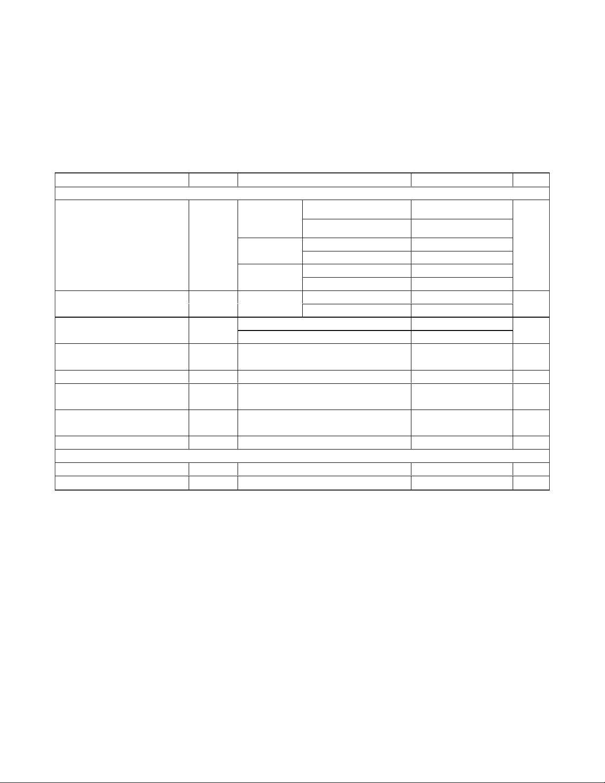
Note 1: All devices are 100% tested at TA= +25°C. Limits over temperature are guaranteed by design.
Note 2: R1 = 215kΩ, R2 = 210kΩ for the MAX4069 only (see
Functional Diagram
). This sets REFOUT to 2.49V nominal.
Note 3: Guaranteed by the PSRR test.
Note 4: The REFOUT voltage for the MAX4069 should be set such that it does not exceed V
CC
- 1.1V. Similarly, the maximum REFIN
voltage for the MAX4072 should also be less than V
CC
- 1.1V.
Note 5: Input-Referred Offset Voltage is defined as the voltage difference between OUT and REFOUT, divided by the selected gain
of either 50 or 100, when V
SENSE
= V
RS+
- V
RS-
= 0V.
Note 6: The negative full-scale sense voltage is limited by the voltage range of OUT from V
REFOUT
to GND.
Note 7: Total OUT Voltage Error is the sum of offset voltage and gain errors. The output voltage is measured relative to the reference
(REFOUT or REFIN).
MAX4069–MAX4072
Maxim Integrated
5
PARAMETER SYMBOL CONDITIONS MIN TYP MAX UNITS
REFOUT (MAX4069/MAX4070/MAX4071)
Reference Output Voltage V
Reference Output Voltage
Temperature Coefficient
Load Regulation
Line Regulation
TCV
ΔV
REFOUT
/ΔI
ΔV
ΔV
REF
REF I
REF/
REF Capacitive-Load Stability 500 pF
Reference Adjust Voltage
Threshold
V
ADJ
Reference Output Voltage Range
Reference Adjust Input Current I
ADJ
REFIN (MAX4072 only)
Input-Voltage Range VCC = 12V 1 4 V
Input Current REFIN = 2.5V, VCC = 12V -60 +20 µA
MAX4069,
= 12V
V
CC
(Note 2)
MAX4070,
V
= 12V
CC
MAX4071,
= 12V
V
CC
REFVCC
CC
= 12V
I
= 0 to 500µA 2
REFOUT
= 0 to -100µA 4
REFOUT
2.7V ≤ VCC ≤ 24V 20 µV/V
MAX4069, V
CC
MAX4069, range adjustable with R1
= 12V
V
CC
MAX4069, VCC = 12V, V
TA = +25°C 2.44 2.49 2.54
= T
MIN
to T
MAX
T
A
2.39 2.59
TA = +25°C 2.45 2.5 2.55
= T
MIN
to T
MAX
T
A
2.40 2.60
TA = +25°C 1.47 1.5 1.53
= T
MIN
to T
MAX
T
A
1.44 1.56
-40°C ≤ TA ≤ +85°C15
T
= T
MIN
to T
MAX
A
20
= 12V 1.230 V
and R2,
V
ADJ
to
+4
= 1.23V 100 nA
ADJ
V
ppm/°C
mV/mA
V
Page 6
Bidirectional, High-Side, Current-Sense
Amplifiers with Reference
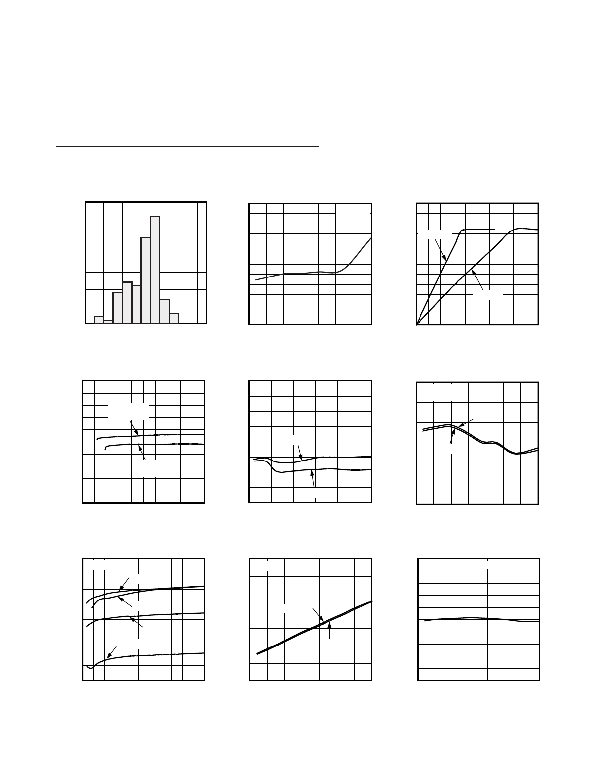
Typical Operating Characteristics
(V
CC
= V
RS+
= 12V, V
SENSE
= 50mV for gain of 100V/V and 75mV for gain of 50V/V, TA = +25°C, unless otherwise noted.)
MAX4069
REFOUT vs. TEMPERATURE
MAX4069-72 toc09
TEMPERATURE (°C)
REFOUT (V)
1007525 500-25
1.205
1.210
1.215
1.220
1.225
1.230
1.235
1.240
1.245
1.250
1.200
-50 125
REFOUT CONNECTED TO ADJ
SUPPLY CURRENT vs. TEMPERATURE
MAX4069-72 toc08
TEMPERATURE (°C)
SUPPLY CURRENT (μA)
1007550250-25
60
80
100
120
140
160
180
40
-50 125
AV = 50V/V
VCC = 24V
VCC = 12V
SUPPLY CURRENT vs. SUPPLY VOLTAGE
MAX4069-72 toc07
SUPPLY VOLTAGE (V)
SUPPLY CURRENT (μA)
22204 6 8 12 14 1610 18
70
80
90
100
110
120
130
140
60
224
AV = 100V/V
MAX4071
MAX4070
MAX4069
MAX4072
TOTAL ERROR vs. TEMPERATURE
MAX4069-72 toc06
TEMPERATURE (°C)
TOTAL ERROR (%)
1007550250-25
-1.0
-0.5
0
0.5
1.0
1.5
-1.5
-50 125
V
SENSE
= 50mV
A
V
= 100V/V
VCC = 24V
VCC = 12V
TOTAL ERROR vs. SUPPLY VOLTAGE
(V
SENSE
= 3mV)
MAX4069-72 toc05
SUPPLY VOLTAGE (V)
TOTAL ERROR (%)
1814610
-1.5
-1.0
-0.5
0
0.5
1.0
1.5
2.0
-2.0
222
AV = 100V/V
AV = 50V/V
TOTAL ERROR vs. SUPPLY VOLTAGE
MAX4069-72 toc04
SUPPLY VOLTAGE (V)
TOTAL ERROR (%)
222016 188 10 12 146
-0.4
-0.3
-0.2
-0.1
0
0.1
0.2
0.3
0.4
0.5
-0.5
424
V
SENSE
= 75mV
A
V
= 50V/V
V
SENSE
= 50mV
A
V
= 100V/V
(V
OUT
- V
REF
) vs. V
SENSE
MAX4069-72 toc03
V
SENSE
(V)
(V
OUT
- V
REF
) (V)
225200150 17550 75 100 12525
1
2
3
4
5
6
7
8
9
10
11
12
0
0 250
AV = 100V/V
AV = 50V/V
INPUT OFFSET VOLTAGE
vs. TEMPERATURE
MAX4069-72 toc02
TEMPERATURE (°C)
INPUT OFFSET VOLTAGE (μV)
1007525 500-25
-125
-100
-75
0
25
50
75
100
125
150
-150
-50 125
-50
-25
AV = 100V/V
INPUT OFFSET VOLTAGE DISTRIBUTION
MAX4069-72 toc01
VOS (μV)
PERCENTAGE OF UNITS (%)
160
120
80
40
0
-40
-80
-120
5
10
15
20
25
0
-160
200
-200
30
35
MAX4069–MAX4072
6
Maxim Integrated
Page 7
Bidirectional, High-Side, Current-Sense
Amplifiers with Reference
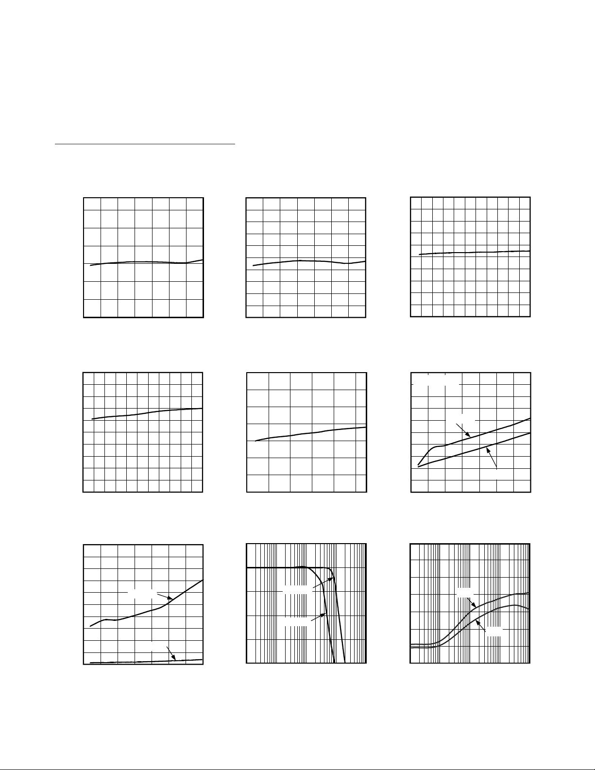
Typical Operating Characteristics (continued)
(V
CC
= V
RS+
= 12V, V
SENSE
= 50mV for gain of 100V/V and 75mV for gain of 50V/V, TA = +25°C, unless otherwise noted.)
0
-140
0.01 1 100.1 100
PSRR AND CMRR vs. FREQUENCY
MAX4069-72 toc18
FREQUENCY (Hz)
PSRR AND CMRR (dB)
-100
-80
-60
-40
-20
-120
CMRR
PSRR
SMALL-SIGNAL GAIN
vs. FREQUENCY
MAX4069-72 toc17
FREQUENCY (kHz)
GAIN (dB)
100101
-15
-10
-5
0
5
-20
0.1 1000
AV = 50V/V
AV = 100V/V
VOL vs. TEMPERATURE
MAX4069-72 toc16
TEMPERATURE (°C)
V
OL
(mV)
1007525 500-25
25
50
75
100
125
150
175
200
225
250
0
-50 125
IL = 500μA
IL = 10μA
VOH vs. TEMPERATURE
MAX4069-72 toc15
TEMPERATURE (°C)
V
OH
(mV)
1007525 500-25
20
40
60
80
100
120
140
160
180
200
0
-50 125
VOH = VCC - V
OUT
IL = 500μA
IL = 10μA
MAX4071
REFOUT vs. SUPPLY VOLTAGE
MAX4069-72 toc14
SUPPLY VOLTAGE (V)
REFOUT (V)
1814106
1.496
1.497
1.498
1.499
1.500
1.501
1.502
1.495
222
MAX4070
REFOUT vs. SUPPLY VOLTAGE
MAX4069-72 toc13
SUPPLY VOLTAGE (V)
REFOUT (V)
222016 186 8 10 12 144
2.491
2.492
2.493
2.494
2.495
2.496
2.497
2.498
2.499
2.500
2.490
224
MAX4069
REFOUT vs. SUPPLY VOLTAGE
MAX4069-72 toc12
SUPPLY VOLTAGE (V)
REFOUT (V)
222016 186 8 10 12 144
1.217
1.219
1.221
1.223
1.225
1.227
1.229
1.231
1.233
1.235
1.215
224
MAX4071
REFOUT vs. TEMPERATURE
MAX4069-72 toc11
TEMPERATURE (°C)
REFOUT (V)
1007525 500-25
1.480
1.485
1.490
1.495
1.500
1.505
1.510
1.515
1.520
1.525
1.475
-50 125
MAX4070
REFOUT vs. TEMPERATURE
MAX4069-72 toc10
TEMPERATURE (°C)
REFOUT (V)
1007550250-25
2.465
2.480
2.495
2.510
2.525
2.540
2.450
-50 125
MAX4069–MAX4072
Maxim Integrated
7
Page 8
Bidirectional, High-Side, Current-Sense
Amplifiers with Reference
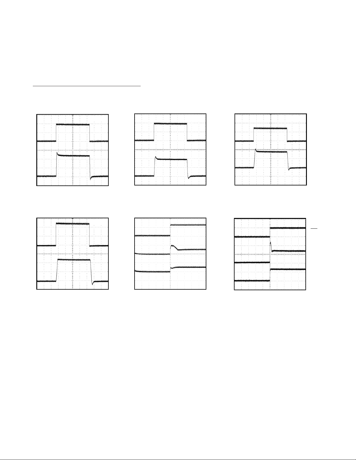
Typical Operating Characteristics (continued)
(V
CC
= V
RS+
= 12V, V
SENSE
= 50mV for gain of 100V/V and 75mV for gain of 50V/V, TA = +25°C, unless otherwise noted.)
EXITING SHUTDOWN
MAX4069-72 toc24
100μs/div
V
REFOUT
2V/div
V
OUT
2V/div
V
SHDN
5V/div
STARTUP DELAY
MAX4069-72 toc23
20μs/div
V
REFOUT
5V/div
V
OUT
5V/div
V
CC
10V/div
LARGE-SIGNAL TRANSIENT RESPONSE
MAX4069-72 toc22
100μs/div
OUTPUT
2V/div
INPUT
20mV/div
GAIN = 100
REF
LARGE-SIGNAL TRANSIENT RESPONSE
MAX4069-72 toc21
100μs/div
OUTPUT
2V/div
INPUT
50mV/div
GAIN = 50
REF
SMALL-SIGNAL TRANSIENT RESPONSE
MAX4069-72 toc20
100μs/div
OUTPUT
500mV/div
REF
INPUT
5mV/div
GAIN = 100
SMALL-SIGNAL TRANSIENT RESPONSE
MAX4069-72 toc19
100μs/div
OUTPUT
200mV/div
REF
INPUT
5mV/div
GAIN = 50
MAX4069–MAX4072
8
Maxim Integrated
Page 9
Bidirectional, High-Side, Current-Sense
Amplifiers with Reference
Functional Diagram
Pin Description
MAX4069–MAX4072
Maxim Integrated
9
PIN
MAX4069
111SHDN
2 2 2 RS- Negative Connection to the External Sense Resistor
3 3 3 RS+ Positive Connection to the External Sense Resistor
4 — — N.C. No Connection. Not internally connected.
5 4 4 GND
6 — — ADJ
7 5 — REFOUT Reference Output Voltage (MAX4069/MAX4070/MAX4071)
8 6 6 OUT
977V
10 8 8 GSEL
— — 5 REFIN Reference Input Voltage (MAX4072)
MAX4070/
MAX4071
MAX4072
NAME FUNCTION
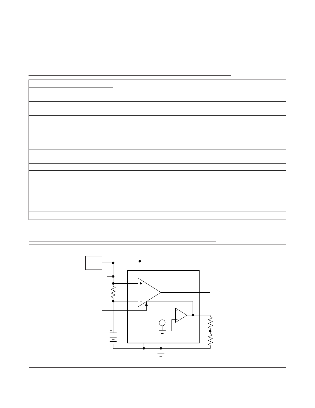
Shutdown Input. Drive SHDN low to select shutdown mode. Connect SHDN
to V
for normal operation.
CC
Ground. For thin QFN packages, also make an external connection from
GND to the under-side exposed paddle.
Adjustable Output Voltage Feedback Input. Connect a resistor-divider
between REFOUT, ADJ, and GND (MAX4069 only, see Functional Diagram).
Voltage Output. The difference voltage, V
the voltage difference between RS+ and RS- and indicates the correct
polarity.
Supply Voltage Input. Bypass VCC to GND with a 0.1µF capacitor.
CC
Gain-Setting Input. Connect GSEL low to select gain = 50V/V, or connect
GSEL high to select gain = 100V/V.
OUT
- V
, is proportional to
REF
LOAD
FROM BATTERY
CHARGER
R
SENSE
GAIN SELECT
SHUTDOWN
2.7V TO 24V
V
RS+
RS-
GSEL
SHDN
CC
MAX4069
OA
OUT TO ADC
REFOUT
ADJ
R1
R2
CSA
GND
V
REF
1.23V
Page 10
Detailed Description
The MAX4069–MAX4072 bidirectional, high-side, current-sense amplifiers are ideal for portable equipment.
The wide 1.35V to 24V input common-mode voltage
range is independent of the supply voltage, ensuring
that the current-sense feedback remains accurate even
when connected to a battery pack in deep discharge.
The MAX4069/MAX4071/MAX4072 operate from a 2.7V
to 24V single supply. Because the MAX4070 has a 2.5V
internal reference, it operates from 3.6V to 24V. All
devices have a low 100µA supply current that reduces
to only 10µA (typ) in shutdown mode. To achieve maximum flexibility, an external current-sense resistor is
used along with a gain select pin (GSEL) to choose
either 50V/V or 100V/V. Drive GSEL low to select gain of
50V/V or drive GSEL high to choose gain of 100V/V
(see
Functional Diagram
). The MAX4069 has an
adjustable reference voltage set by two external resistors between REFOUT and ADJ, and GND pins. The
MAX4070 contains an internal 2.5V reference. The
MAX4071 is similar to the MAX4070 but with a fixed
internal reference voltage of 1.5V. The MAX4072 has a
reference input pin to allow use of external references.
Charging current is represented by an output voltage
from the reference voltage to VCC, while discharge current is given from the reference voltage to GND. The
direction of V
SENSE
is totally arbitrary.
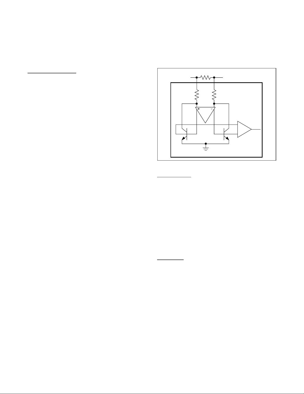
The input stage of the MAX4069–MAX4072 is shown in
Figure 1. Its unique topology allows for monitoring bidirectional currents through the sense resistor (R
SENSE
). If,
for instance, current flows from RS+ to RS-, the
MAX4069–MAX4072 match for the voltage drop over the
external sense resistor (R
SENSE
) by increasing the current through the internal Q1 and RG1. At the same time,
the current through Q2 and RG2 decreases, however,
internal circuitry not shown in Figure 1 prevents Q2 from
turning off completely. Likewise, if current flows from RSto RS+, the current through Q2 and RG2 increases and
the current through Q1 decreases. In this way, the voltages at the input terminals of the internal amplifier A1 are
kept constant and an accurate measurement of the sense
voltage is achieved. In the following amplifier stages of
the MAX4069–MAX4072, the output signal of amplifier A2
is level-shifted towards the reference voltage (V
REF
),
resulting in a voltage at the output pin (OUT) that swings
above the V
REF
voltage for positive-sense voltages and
below V
REF
for negative-sense voltages.
Applications Information
Bidirectional, Current-Sense Amplifier
Systems such as laptop computers and other devices
that have internal charge circuitry require a precise bidirectional, current-sense amplifier to accurately monitor
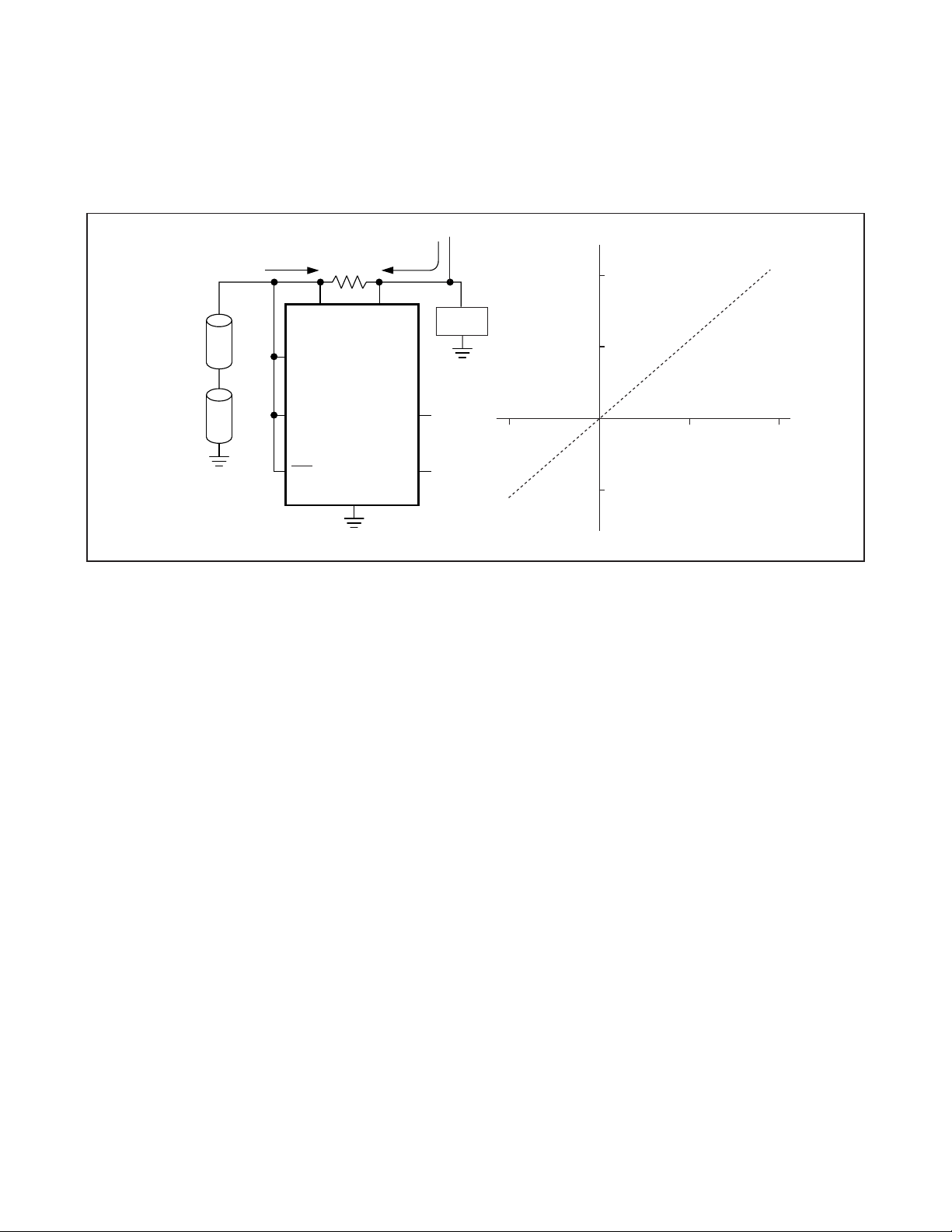
the battery’s current regardless of polarity. Figure 2
shows the MAX4069–MAX4072 used as a bidirectional
current monitor. In Figure 2, the direction of V
SENSE
is
assigned to charge and discharge, assuming charge is
greater than discharge. The practical choice of direction
is based on dynamic range at OUT, given that the range
of REF to VCCis usually greater than from REF to
ground. This is useful for implementing either smart battery packs or fuel gauges.
High-Current Measurement
The MAX4069–MAX4072 can achieve high-current
measurements by using low-value sense resistors,
which can be paralleled to further increase the currentsense limit.
Adjusting V
REF
(MAX4069)
The MAX4069 has an output reference voltage that can
be set to a desired voltage by a two-resistor divider
between REFOUT, ADJ, and GND. If REFOUT and ADJ
are connected together, the minimum output reference
voltage is obtained, 1.23V (typ). The maximum voltage
for REFOUT is 4V (that requires VCC≥ 5.1V). The recommended range for the external resistors is: R1 + R2
should be > 20kΩ and < 500kΩ.
Bidirectional, High-Side, Current-Sense
Amplifiers with Reference
Figure 1. Detailed Input Stage
Note: RG1= RG2= 104k (typ).
MAX4069–MAX4072
10
Maxim Integrated
R
Q1 Q2
SENSE
RS-RS+
RG2RG1
A1
MAX4069–MAX4072
OUT
I
OUT
A2
Page 11
External Reference (MAX4072)
The MAX4072 contains REFIN pin for external reference voltage. The allowable voltage range on REFIN is
1V (min) to 4V (max) with VCC≥ 5.1V.
Reference Output
(MAX4069/MAX4060/MAX4071)
The REFOUT of the MAX4069/MAX4070/MAX4071 can
sink 100µA and source 500µA. Keep the total capacitance on REFOUT under 500pF to maintain stability.
Recommended Component Values
Ideally, the maximum load current develops the fullscale sense voltage across the current-sense resistor.
Choose the gain needed to yield the maximum output
voltage required for the application:
V
OUT
= V
SENSE
x A
V
where V
SENSE
is the full-scale sense voltage, 75mV for
gain of 50V/V, or 50mV for gain of 100V/V. AVis the
gain of the device.
In applications monitoring high current, ensure that
R
SENSE
is able to dissipate its own I2R loss. If the resistor’s power dissipation is exceeded, its value may drift
or it may fail altogether, causing a differential voltage
across the terminals in excess of the absolute maximum ratings. Use resistors specified for current- sensing applications.
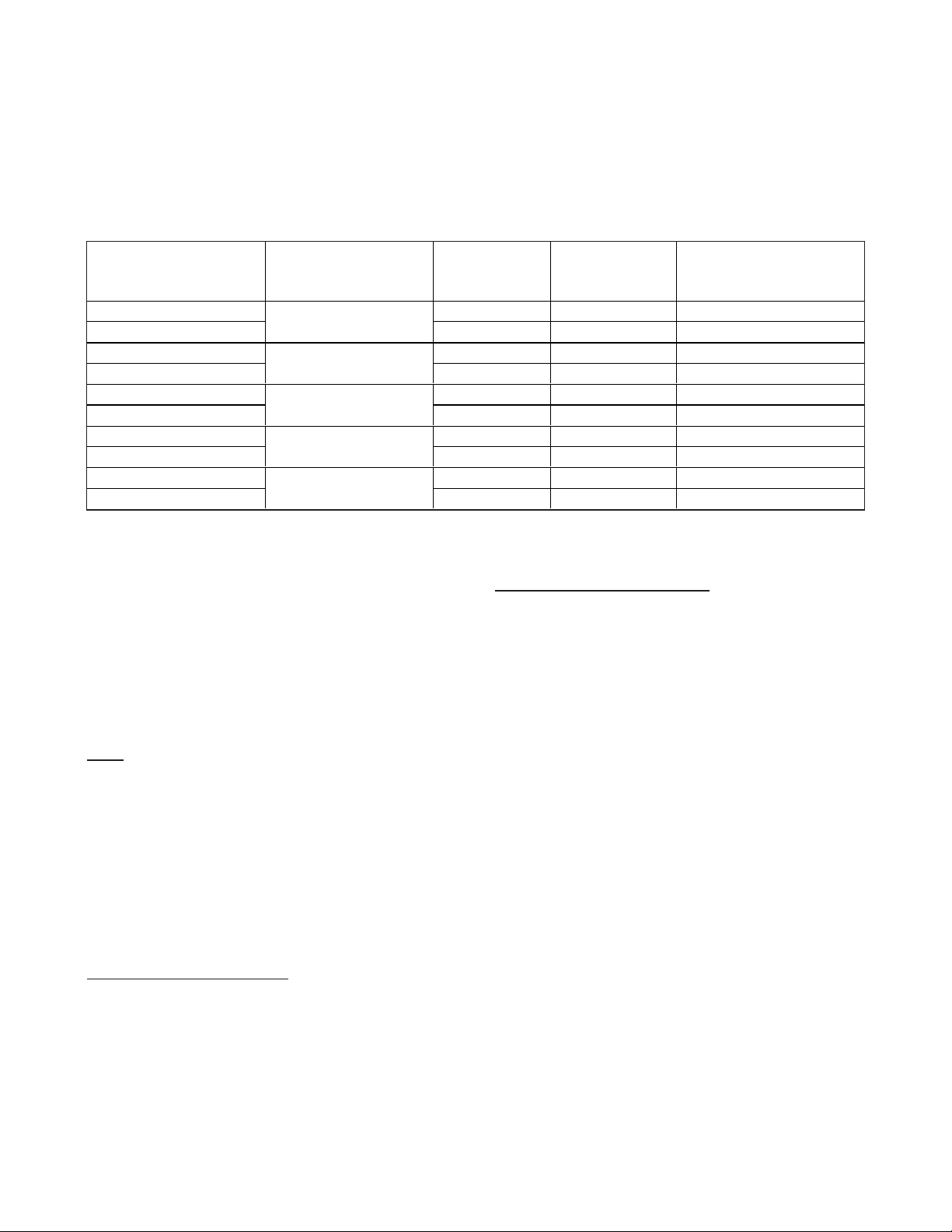
The MAX4069–MAX4072 sense a wide variety of currents with different sense-resistor values. Table 1 lists
common resistor values for typical operation of these
devices. Listed output voltage is with respect to REF.
Sense Resistor, R
SENSE
Choose R
SENSE
based on the following criteria:
Voltage Loss: A high R
SENSE
value causes the powersource voltage to degrade through IR loss. For minimal
voltage loss, use the lowest R
SENSE
value.
Accuracy: A high R
SENSE
value allows lower currents
to be measured more accurately. This is because offsets become less significant when the sense voltage is
larger. For best performance, select R
SENSE
to provide
approximately 75mV (gain of 50V/V) or 50mV (gain of
100V/V) of sense voltage for the full-scale current in
each application.
Efficiency and Power Dissipation: At high-current levels, the I2R losses in R
SENSE
can be significant. Take
this into consideration when choosing the resistor value
and its power dissipation (wattage) rating. Also, the
sense resistor’s value might drift if it is allowed to heat
up excessively.
Inductance: Keep inductance low if I
SENSE
has a large
high-frequency component. Wire-wound resistors have
the highest inductance, while metal film is somewhat
better. Low-inductance metal-film resistors are also
available. Instead of being spiral-wrapped round a
Bidirectional, High-Side, Current-Sense
Amplifiers with Reference
2
Figure 2. Bidirectional Current Monitor
MAX4069–MAX4072
Maxim Integrated
11
CELLS
I
I
DISCHARGE
RS- RS+
V
CC
GSEL
R
SENSE
MAX4070
CHARGE
OUT
LOAD
TO ADC
V
- V
OUT
REF
-25mV 25mV 50mV0
5V
2.5V
A
= 100
V
V
SENSE
CHARGE
CURRENT
GND
REFOUT
2.5V
SHDN
DISCHARGE
CURRENT
-2.5V
Page 12
Bidirectional, High-Side, Current-Sense
Amplifiers with Reference
core, as in metal-film or wire-wound resistors, they are
a straight band of metal and are available in values
under 1Ω.
Peak Current: The maximum current through R
SENSE
must be limited to:
I
PEAK
= 0.3V / (R
SENSE
+ R
TRACE
)
where R
TRACE
is the total stray resistance from RS+
and RS- to R
SENSE
. To prevent forwarding the back-toback diodes between the differential input, the absolute
maximum of the differential input voltage is 0.3V.
Dynamic Range Considerations
Although the MAX4069–MAX4072 have fully symmetrical, bidirectional, V
SENSE
input capability, the outputvoltage range is usually higher from REF to VCCand
lower from REF to GND (unless the supply voltage is at
the lowest end of the operating range). Therefore, the
user must consider the dynamic range of current monitored in both directions and choose the supply voltage
and the reference voltage (REFOUT or REFIN) to make
sure the output swing above and below REF is adequate to handle the swings without clipping or running
out of headroom.
Shutdown Mode
When SHDN is low, the MAX4069–MAX4072 are shut
down and consume only 10µA. In shutdown mode,
OUT is high impedance and turns off. Connect SHDN
to VCCfor normal operation.
Power-Supply Bypassing
and Grounding
The MAX4069–MAX4072 do not require special
bypassing and respond quickly to transient changes in
line current. You can place a large capacitor at the RSterminal (or “load” side) to decouple the load and,
thereby, reduce the current transients. These capacitors are not required for operation or stability and their
use does not degrade performance.
The MAX4069–MAX4072 have been designed as a highside current monitor to ease the task of grounding any
battery charger, thermistor, etc., that may be a part of
the battery pack. Grounding these devices requires no
special precautions; follow the same cautionary steps
that apply to the system as a whole. High-current systems can experience large voltage drops across a
ground plane, and this drop may add to or subtract from
V
OUT.
Using differential measurement between V
OUT
and REF prevents this problem. For highest current-measurement accuracy, use a single-point star ground.
On thin QFN packages, there is an exposed paddle that
does not carry any current, but should also be connected to the ground plane for rated power dissipation.
Table 1. Recommended Component Values
MAX4069–MAX4072
12
Maxim Integrated
FULL-SCALE
CURRENT
(A)
0.075 50 75 3.75
0.05
0.75 50 75 3.75
0.5
3.75 50 75 3.75
2.5
7.5 50 75 3.75
5.0
15.0 50 75 3.75
10.0
CURRENT-SENSE
RESISTOR (mΩ)
1000
100
20
10
5
GAIN
(V/V)
100 50 5.0
100 50 5.0
100 50 5.0
100 50 5.0
100 50 5.0
V
SENSE
(mV)
FULL-SCALE OUTPUT
VOLTAGE WITH RESPECT
TO REF (V)
Page 13
Layout
In order to dissipate sense-resistor heat from large
sense currents, solder the RS+ and the RS- pins to
large copper traces. Keep the part away from other
heat-generating devices.
For accurate measurement of V
SENSE
, the Kelvin
method is recommended. The current into RS+ and RSis only a few microamps; therefore, a short distance from
RS+ and RS- pins does not cause significant errors. It is
recommended to keep the value of R
SENSE
reasonably
higher than the values of the trace’s resistance.
Bidirectional, High-Side, Current-Sense
Amplifiers with Reference
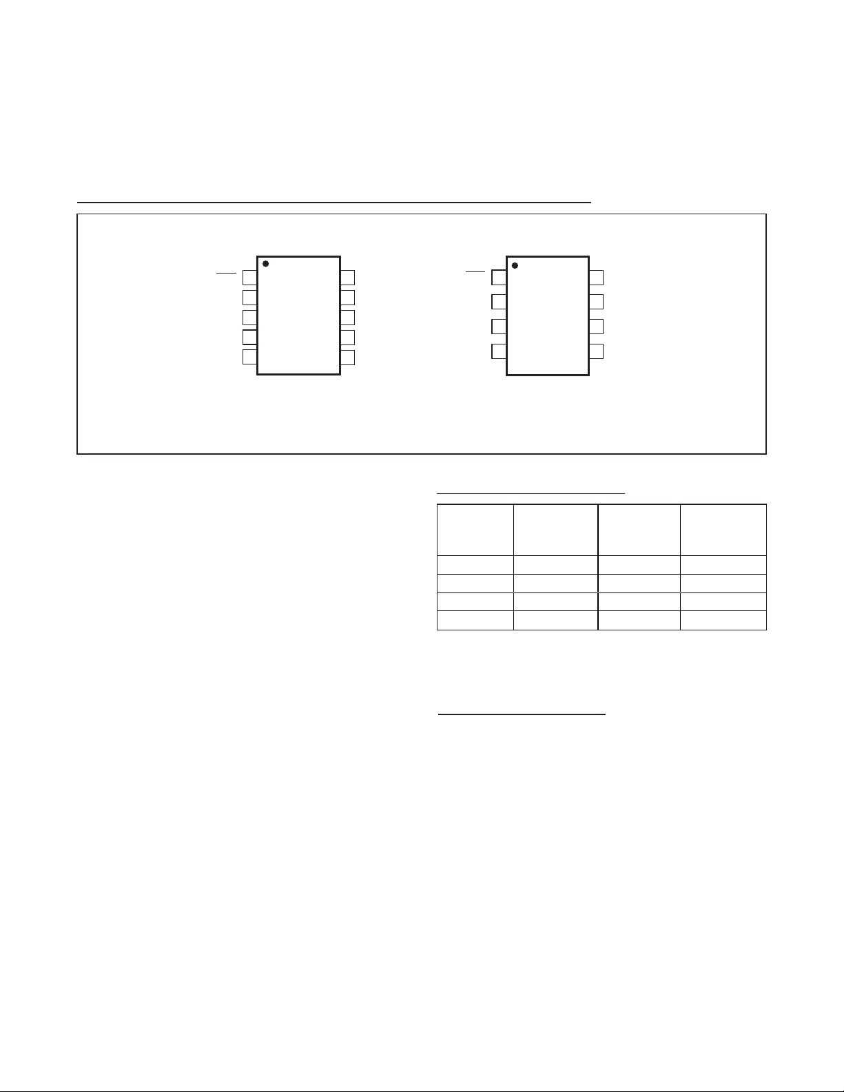
Pin Configurations
Chip Information
TRANSISTOR COUNT: 338
PROCESS: BiCMOS
Selector Guide
MAX4069–MAX4072
Maxim Integrated
13
TOP VIEW
SHDN
RS-
RS+
1
2
MAX4069
3
4
5
μMAX
10
GSEL
9
V
CC
OUT
8
REFOUTN.C.
7
ADJGND
6
1
SHDN
RS-
2
MAX4070
MAX4071
3
RS+
GND
(REFIN) FOR MAX4072 ONLY.
MAX4072
4
Thin QFN/μMAX
87GSEL
V
CC
OUT
6
REFOUT (REFIN)
5
SUPPLY
PART REFERENCE
MAX4069 ADJUSTABLE 2.7 to 24 1.35 to 24
MAX4070 2.5V 3.6 to 24 1.35 to 24
MAX4071 1.5V 2.7 to 24 1.35 to 24
MAX4072 EXTERNAL 2.7 to 24 1.35 to 24
VOLTAGE
RANGE (V)
COMMON-
MODE RANGE
(V)
Page 14
Bidirectional, High-Side, Current-Sense
Amplifiers with Reference
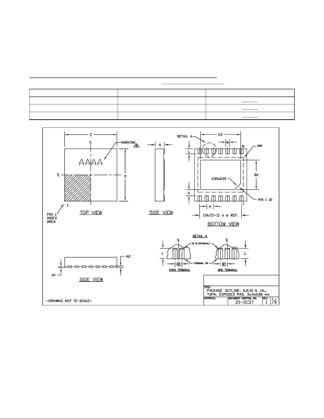
Package Information
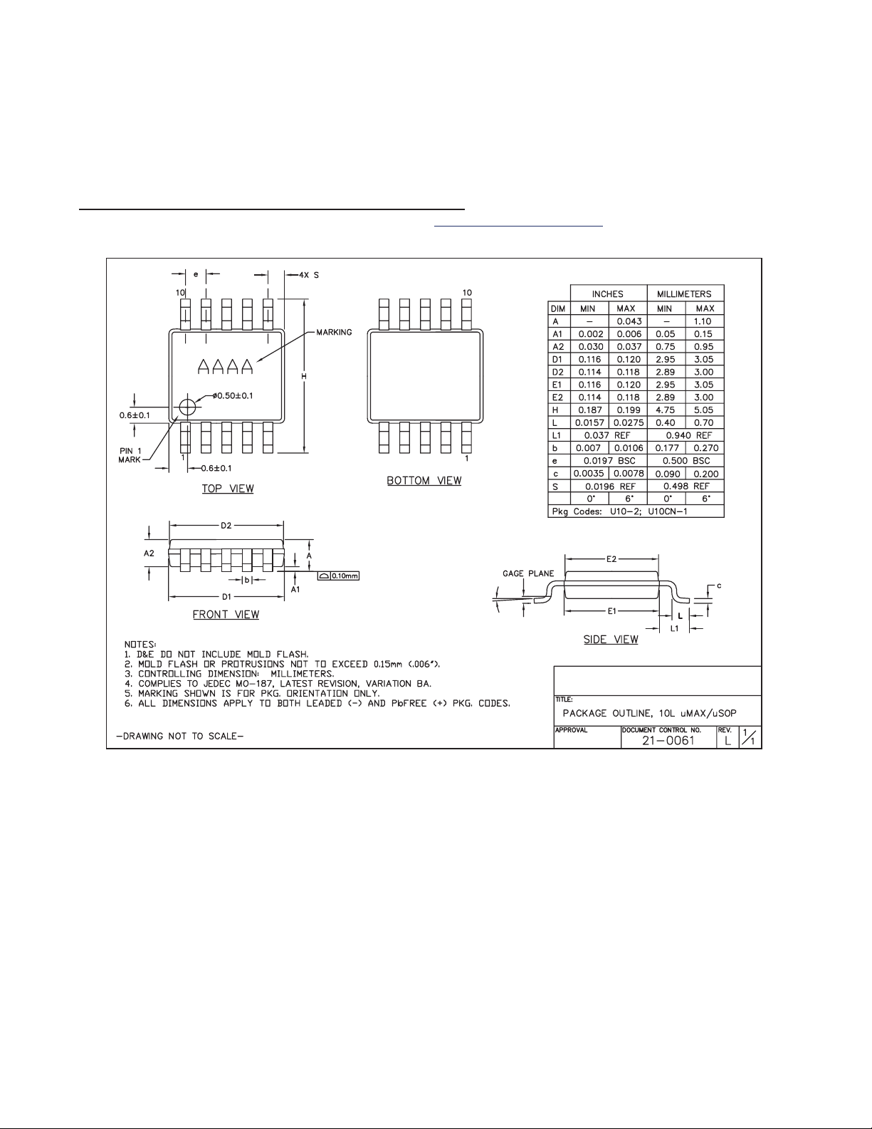
For the latest package outline information and land patterns, go to www.maxim-ic.com/packages.
PACKAGE TYPE PACKAGE CODE DOCUMENT NO.
8 TQFN-EP T833-2
21-0137
8 µMAX U8-1
21-0036
10 µMAX U10-2
21-0061
MAX4069–MAX4072
14
Maxim Integrated
6, 8, &10L, DFN THIN.EPS
Page 15
Bidirectional, High-Side, Current-Sense
Amplifiers with Reference
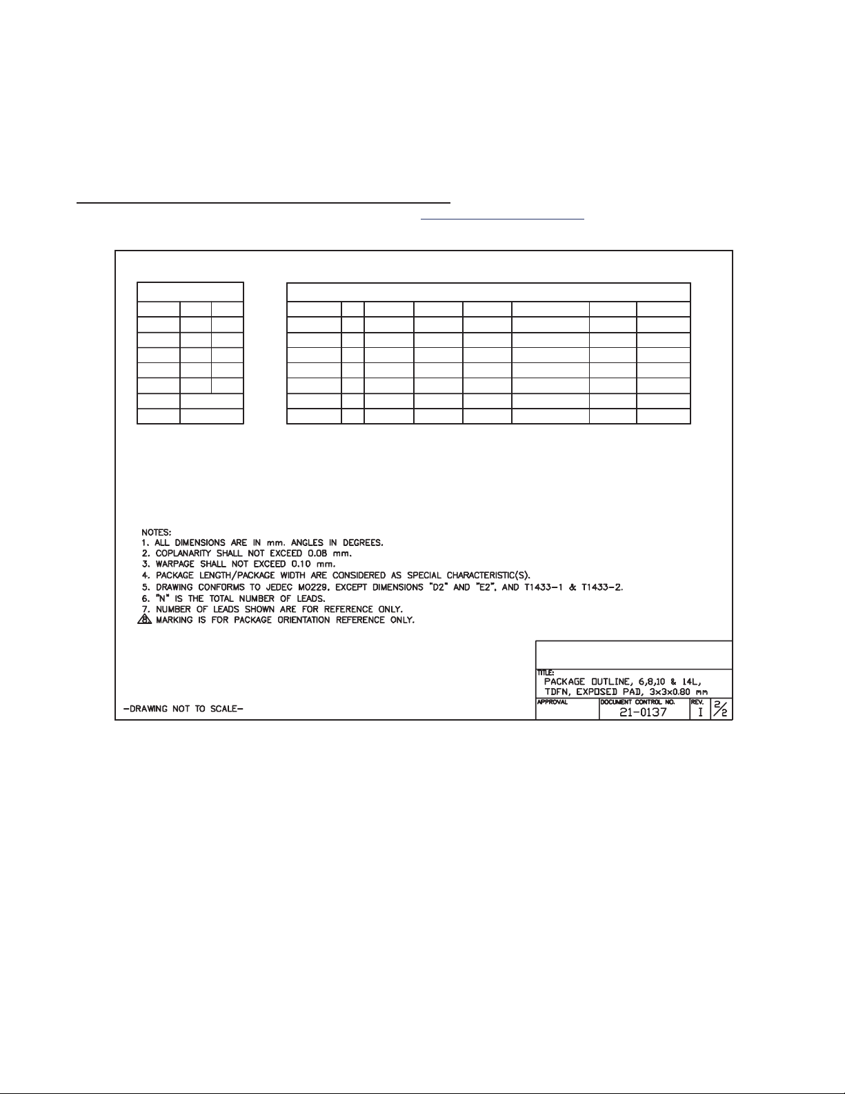
Package Information (continued)
For the latest package outline information and land patterns, go to www.maxim-ic.com/packages.
MAX4069–MAX4072
Maxim Integrated
15
COMMON DIMENSIONS
SYMBOL MIN. MAX.
A 0.70 0.80
D 2.90 3.10
E 2.90 3.10
A1
0.00 0.05
L 0.20 0.40
0.25 MIN.k
A2 0.20 REF.
PACKAGE VARIATIONS
PKG. CODE N D2 E2 e JEDEC SPEC b
T633-2 6 1.50±0.10 2.30±0.10 0.95 BSC MO229 / WEEA 0.40±0.05 1.90 REF
T833-2 8 1.50±0.10 2.30±0.10 0.65 BSC MO229 / WEEC 0.30±0.05 1.95 REF
T833-3 8 1.50±0.10 2.30±0.10 0.65 BSC MO229 / WEEC 0.30±0.05 1.95 REF
1.50±0.10 MO229 / WEED-3
2.30±0.10 MO229 / WEED-3 2.00 REF0.25±0.050.50 BSC1.50±0.1010T1033-2
0.40 BSC - - - - 0.20±0.05 2.40 REFT1433-2 14 2.30±0.101.70±0.10
[(N/2)-1] x e
2.00 REF0.25±0.050.50 BSC2.30±0.1010T1033-1
2.40 REF0.20±0.05- - - - 0.40 BSC1.70±0.10 2.30±0.1014T1433-1
Page 16
Bidirectional, High-Side, Current-Sense
Amplifiers with Reference
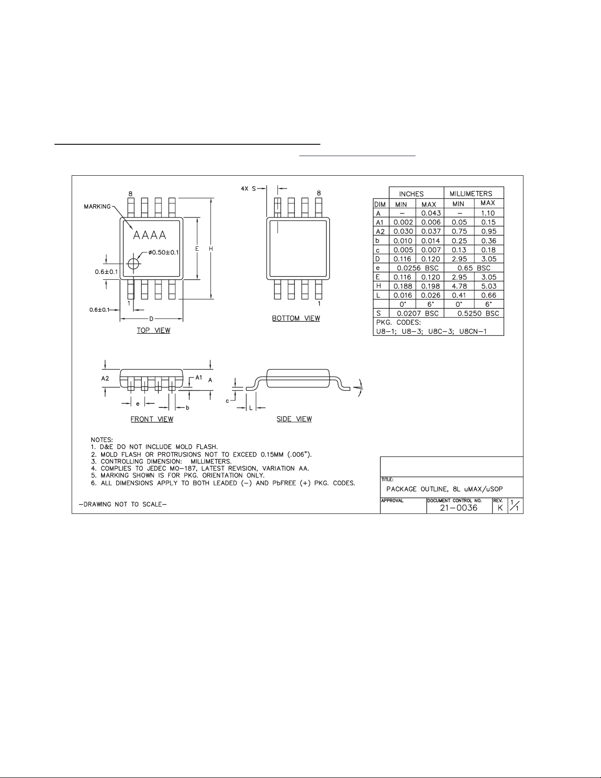
Package Information (continued)
For the latest package outline information and land patterns, go to www.maxim-ic.com/packages.
MAX4069–MAX4072
16
Maxim Integrated
α
8LUMAXD.EPS
α
Page 17
Bidirectional, High-Side, Current-Sense
Amplifiers with Reference
Package Information (continued)
For the latest package outline information and land patterns, go to www.maxim-ic.com/packages.
MAX4069–MAX4072
Maxim Integrated
17
α
10LUMAX.EPS
α
Page 18
Bidirectional, High-Side, Current-Sense
Amplifiers with Reference
Revision History
MAX4069–MAX4072
18
Maxim Integrated 160 Rio Robles, San Jose, CA 95134 USA 1-408-601-1000
Maxim cannot assume responsibility for use of any circuitry other than circuitry entirely embodied in a Maxim product. No circuit patent licenses are implied.
Maxim reserves the right to change the circuitry and specifications without notice at any time. The parametric values (min and max limits) shown in the Electrical
Characteristics table are guaranteed. Other parametric values quoted in this data sheet are provided for guidance.
©
2008 Maxim Integrated
The Maxim logo and Maxim Integrated are trademarks of Maxim Integrated Products, Inc.
REVISION
NUMBER
3 11/08 Added information for RG1 and RG2 10
REVISION
DATE
DESCRIPTION
PAGES
CHANGED
 Loading...