

Page 1
General Description
The MAX3890 serializer is ideal for converting 16-bitwide, 155Mbps parallel data to 2.5Gbps serial data in
ATM and SDH/SONET applications. Operating from a
single +3.3V supply, this device accepts low-voltage
differential-signal (LVDS) clock and data inputs for
interfacing with high-speed digital circuitry, and delivers PECL serial data and clock outputs. A fully integrated PLL synthesizes an internal 2.5GHz serial clock from
a 155.52MHz, 77.76MHz, 51.84MHz, or 38.88MHz reference clock. A loopback data output is provided to
facilitate system diagnostic testing.
The MAX3890 is available in the extended temperature
range (-40°C to +85°C) in a 64-pin TQFP exposedpaddle (EP) package.
Applications
2.5Gbps SDH/SONET Transmission Systems
2.5Gbps ATM/SONET Access Nodes
Add/Drop Multiplexers
Digital Cross-Connects
ATM Backplanes
Features
♦ Single +3.3V Supply
♦ 495mW Power Consumption
♦ Exceeds ANSI, ITU, and Bellcore Specifications
♦ 155Mbps (16-bit wide) Parallel to 2.5Gbps Serial
Conversion
♦ Clock Synthesis for 2.5Gbps
♦ Multiple Clock Reference Frequencies
(155.52MHz, 77.76MHz, 51.84MHz, 38.88MHz)
♦ LVDS Parallel Clock and Data Inputs
♦ Additional High-Speed Output for System
Loopback Testing
MAX3890
+3.3V, 2.5Gbps, SDH/SONET 16:1 Serializer
with Clock Synthesis and LVDS Inputs
________________________________________________________________
Maxim Integrated Products
1
Typical Operating Circuit
19-1498; Rev 0; 6/99
PART
MAX3890ECB -40°C to +85°C
TEMP. RANGE PIN-PACKAGE
64 TQFP-EP*
Ordering Information
For free samples & the latest literature: http://www.maxim-ic.com, or phone 1-800-998-8800.
For small orders, phone 1-800-835-8769.
Pin Configuration appears at end of data sheet.
EVALUATION KIT
AVAILABLE
*
EP = Exposed Paddle
155MHz REF. CLOCK INPUT
OVERHEAD
GENERATION
+3.3V
RCLK+ RCLK- V
PDI0+
PDI0-
PDI15+
PDI15-
PCLKI+
PCLKI-
PCLKO+
PCLKO-
GND
THIS SYMBOL REPRESENTS A TRANSMISSION LINE
OF CHARACTERISTIC IMPEDANCE (Z
FIL+
MAX3890
330nF
FIL-
CLKSET
SLBO+
= 50Ω).
0
CC
SLBO-
TTL
SOS
SDO+
SDO-
SCLKO+
SCLKO-
+3.3V
130Ω
82Ω
OPTIONAL CONNECTION TO MAX3880
FOR SYSTEM LOOPBACK TESTING.
130Ω
82Ω
+3.3V
130Ω
82Ω
130Ω
82Ω
+3.3V
V
CC
MAX3867
Page 2
MAX3890
+3.3V, 2.5Gbps, SDH/SONET 16:1 Serializer
with Clock Synthesis and LVDS Inputs
2 _______________________________________________________________________________________
ABSOLUTE MAXIMUM RATINGS
DC ELECTRICAL CHARACTERISTICS
(VCC= +3.0V to +3.6V, differential LVDS loads = 100Ω ±1%, PECL loads = 50Ω ±1% to (V
CC
- 2V), CML loads = 50Ω ±1% to VCC,
T
A
= -40°C to +85°C, unless otherwise noted. Typical values are at VCC= +3.3V, TA= +25°C.)
Stresses beyond those listed under “Absolute Maximum Ratings” may cause permanent damage to the device. These are stress ratings only, and functional
operation of the device at these or any other conditions beyond those indicated in the operational sections of the specifications is not implied. Exposure to
absolute maximum rating conditions for extended periods may affect device reliability.
Terminal Voltage (with respect to GND)
V
CC
.......................................................................-0.5V to +5V
All Inputs, FIL+, FIL-...............................-0.5V to (V
CC
+ 0.5V)
Output Current
LVDS Outputs (PCLKO±)................................................10mA
PECL Outputs (SDO±, SCLKO±)....................................50mA
CML Outputs (SLBO±)....................................................15mA
Continuous Power Dissipation (T
A
= +85°C)
TQFP-EP (derate 44.8mW/°C above +85°C) ......................1W
Operating Temperature Range ...........................-40°C to +85°C
Storage Temperature Range .............................-60°C to +150°C
Lead Temperature (soldering, 10sec) .............................+300°C
T
A
= 0°C to +85°C
PECL outputs unterminated,
SOS = low
TA= 0°C to +85°C
Differential input voltage = 100mV
CONDITIONS
V
VCC- 1.025 VCC- 0.88
V
OH
Output Voltage High
mA150 230I
CC
Supply Current
V0.925V
OL
Output Voltage Low
V1.475V
OH
Output Voltage High
Ω
85 100 115R
IN
Differential Input Resistance
mV60V
HYST
Threshold Hysteresis
V
VCC- 1.81 VCC- 1.62
V
OL
Output Voltage Low
V0 2.4V
I
Input Voltage Range
mV-100 100V
IDTH
Differential Input Threshold
UNITSMIN TYP MAXSYMBOLPARAMETER
Figure 5
%±2.5 ±10
∆R
O
Change in Magnitude of Single-Ended
Output Resistance for Complementary
Outputs
Ω
40 95 140R
O
Single-Ended Output Resistance
mV±25
∆V
OS
Change in Magnitude of Output Offset
Voltage for Complementary States
mV250 400
|VOD|
Differential Output Voltage
mV±25
∆|VOD|
Change in Magnitude of Differential
Output Voltage for Complementary
States
V1.125 1.275V
OS
Output Offset Voltage
TA= -40°C V
CC
- 1.085 VCC- 0.88
TA= -40°C VCC-1.83 VCC- 1.555
PECL OUTPUTS (SDO±, SCLKO±)
LVDS INPUTS AND OUTPUTS (PCLKO±, PDI_±, PCLKI±, RCLKI±)
Page 3
MAX3890
+3.3V, 2.5Gbps, SDH/SONET 16:1 Serializer
with Clock Synthesis and LVDS Inputs
_______________________________________________________________________________________ 3
Note 1: AC characteristics guaranteed by design and characterization.
Note 2: Setup and hold times are relative to the rising edge of PCLKI+, measured by applying a 155.52MHz differential parallel
clock with rise/fall time = 1ns (20% to 80%). See Figure 2.
Note 3: For f
RCLK
= 38.88MHz, the minimum reference clock amplitude is ≥ 200mV.
(Note 2)
(Note 2)
Figure 2
Jitter bandwidth = 12kHz to 20MHz,
RCLK amplitude >
|V
IDTH
| (Note 3)
20% to 80%
CONDITIONS
ps700t
H
Parallel Data-Hold Time
ps300t
SU
GHz2.488f
SCLK
Serial Clock Rate
Parallel Data Setup Time
ns0 +4.0t
SKEW
PCLKO to PCLKI Skew
ps
RMS
3
Φ
0
Output Jitter Generation (SCLKO±)
ps120t
R, tF
PECL Differential Output Rise/Fall
Time
UNITSMIN TYP MAXSYMBOLPARAMETER
AC ELECTRICAL CHARACTERISTICS
(VCC= +3.0V to +3.6V, differential LVDS load = 100Ω ±1%, PECL loads = 50Ω ±1% to (V
CC
- 2V), CML loads = 50Ω ±1% to VCC,
T
A
= -40°C to +85°C, unless otherwise noted. Typical values are at VCC= +3.3V, TA= +25°C.) (Note 1)
MHz155.52f
PCLKI
Parallel Input Clock Rate
20% to 80%, f = 155.52MHz ns1.0
t
R
, t
F
Reference Clock Input (RCLKI)
Rise/Fall Time
20% to 80% ns1.0
t
R
, t
F
Parallel Clock Output (PCLKO)
Rise/Fall Time
SCLKO rising edge to SDO edge ps110 290t
SCLK-SD
Serial Clock Output (SCLKO) to
Serial-Data Output (SDO) Delay
DC ELECTRICAL CHARACTERISTICS (continued)
(VCC= +3.0V to +3.6V, differential LVDS loads = 100Ω ±1%, PECL loads = 50Ω ±1% to (V
CC
- 2V), CML loads = 50Ω ±1% to V
CC,
TA= -40°C to +85°C, unless otherwise noted. Typical values are at VCC= +3.3V, TA= +25°C.)
CONDITIONS
µA-10 10I
IL
V0.8V
IL
Input Voltage Low
µA-10 10I
IH
Input Current High
Input Current Low
UNITSMIN TYP MAXSYMBOLPARAMETER
Ω50R
O
Single-Ended Output Resistance
mV100 400
|VOD|
Differential Output Voltage
CLKSET = 0 or V
CC
µA±500I
CLKSET
CLKSET Input Current
V2.0V
IH
Input Voltage High
TTL INPUT (SOS)
PROGRAMMING INPUT (CLKSET)
CURRENT MODE LOGIC (CML) OUTPUTS (SLBO±)
Page 4
MAX3890
+3.3V, 2.5Gbps, SDH/SONET 16:1 Serializer
with Clock Synthesis and LVDS Inputs
4 _______________________________________________________________________________________
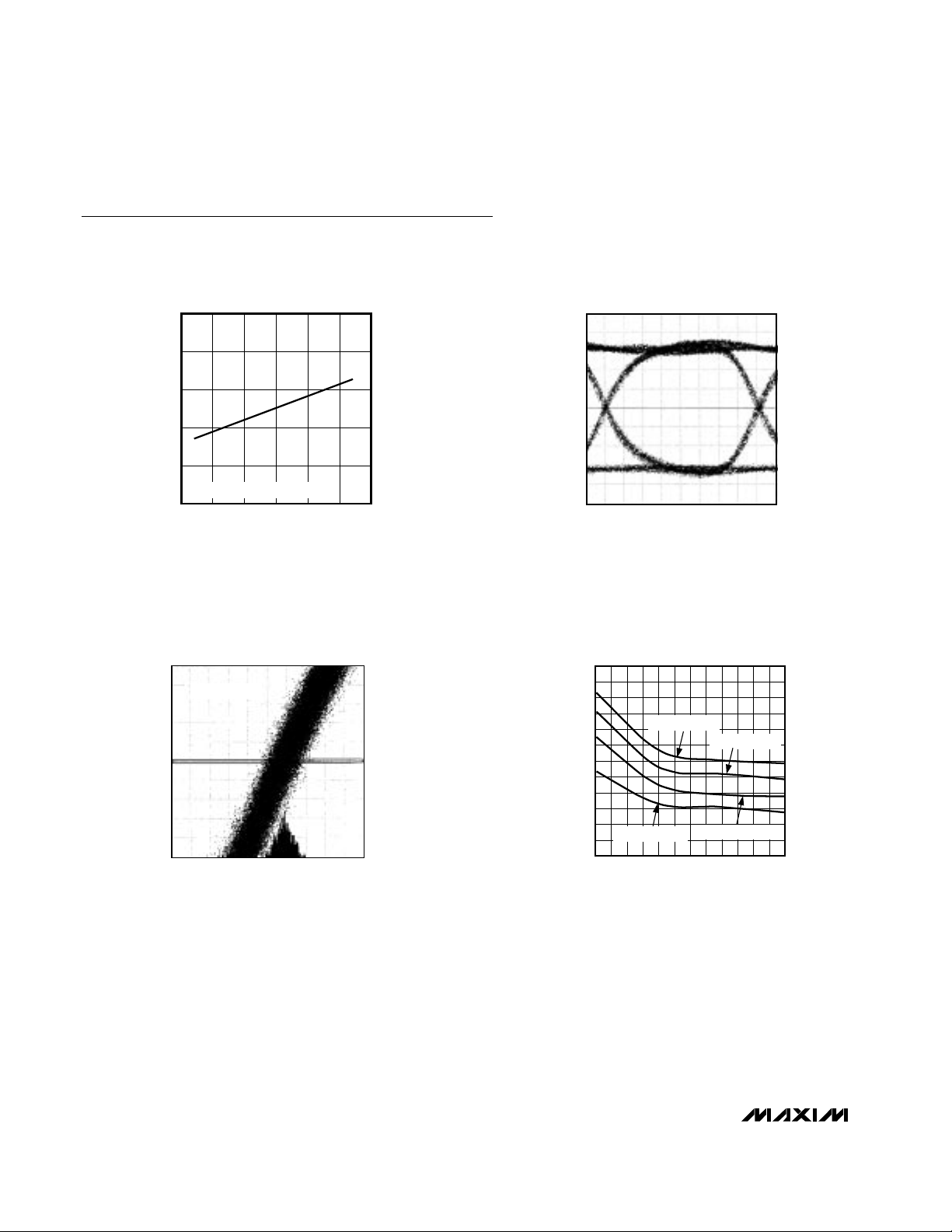
Typical Operating Characteristics
(VCC= +3.3V, PECL loads = 50Ω ±1%, TA= +25°C, unless otherwise noted.)
SUPPLY CURRENT
200
vs. TEMPERATURE
SERIAL-DATA OUTPUT EYE DIAGRAM
180
160
140
SUPPLY CURRENT (mA)
120
PECL OUTPUTS UNTERMINATED
100
-50 -25 25 100
SERIAL-DATA OUTPUT JITTER
f
RCK
050
TEMPERATURE (°C)
= 155.52MHz
MAX3890-01
75
50ps/div
MAX3890-02
OUTPUT JITTER GENERATION
vs. RCLK AMPLITUDE
f
= 38.88MHz
RCLK
f
RCLK
MAX3890 toc04
= 51.84MHz
MAX3890-03
3.0
2.5
2.0
1.5
1.0
f
= 155.52MHz
RCK
5ps/div
TOTAL WIDEBAND RMS JITTER = 2.155ps,
PEAK-TO-PEAK JITTER = 15.7ps
OUTPUT JITTER GENERATION (ps)
0.5
f
= 155.52MHz
RCLK
0
100 150 200 250 300 350 400
RCLK AMPLITUDE (mV)
f
RCLK
= 77.76MHz
Page 5

MAX3890
+3.3V, 2.5Gbps, SDH/SONET 16:1 Serializer
with Clock Synthesis and LVDS Inputs
_______________________________________________________________________________________ 5
Pin Description
NAME FUNCTION
1, 17, 33, 48, 49, 63 GND Ground
2, 5, 7, 10, 13,
14, 32, 56, 60, 64
V
CC
+3.3V Supply Voltage
PIN
3 SLBO- System Loopback Inverting Output. Enabled when SOS is high.
4 SLBO+ System Loopback Noninverting Output. Enabled when SOS is high.
12 SDO+ Noninverting PECL Serial-Data Output
9 SCLKO+ Noninverting PECL Serial Clock Output
6 SOS System Loopback Output Select. System loopback disabled when low.
55 PCLKO-
Inverting LVDS Parallel Clock Output. Use positive transition of PCLKO to clock the overhead management circuit.
54 PCLKO+
Noninverting LVDS Parallel Clock Output. Use positive transition of PCLKO to clock the
overhead management circuit.
57 RCLK+
Noninverting LVDS Reference Clock Input. Connect an LVDS-compatible crystal reference clock to the RCLK inputs.
59 CLKSET
Reference Clock Rate Programming Pin:
CLKSET = VCC: Reference Clock Rate = 155.52MHz
CLKSET = Open: Reference Clock Rate = 77.76MHz
CLKSET = 20kΩ to GND: Reference Clock Rate = 51.84MHz
CLKSET = GND: Reference Clock Rate = 38.88MHz
58 RCLK-
Inverting LVDS Reference Clock Input. Connect an LVDS-compatible crystal reference
clock to the RCLK inputs.
61 FIL- Filter Capacitor Input. Connect a 330nF capacitor between FIL+ and FIL-.
18, 20, 22, 24, 26,
28, 30, 34, 36, 38,
40, 42, 44, 46, 50, 52
PDI15+ to
PDI0+
Noninverting LVDS Parallel Data Inputs. Data is clocked on the PCLKI positive transition.
62 FIL+ Filter Capacitor Input. Connect a 330nF capacitor between FIL+ and FIL-.
8 SCLKO- Inverting PECL Serial Clock Output
11 SDO- Inverting PECL Serial-Data Output
15 PCLKI+
Noninverting LVDS Parallel Clock Input. Connect the incoming parallel-clock signal to the
PCLKI inputs. Note that data is updated on the positive transition of the PCLKI signal.
16 PCLKI-
Inverting LVDS Parallel Clock Input. Connect the incoming parallel-clock signal to the PCLKI
inputs. Note that data is updated on the positive transition of the PCLKI signal.
19, 21, 23, 25, 27,
29, 31, 35, 37, 39,
41, 43, 45, 47, 51, 53
PDI15- to
PDI0-
Inverting LVDS Parallel Data Inputs. Data is clocked on the PCLKI positive transition.
Page 6

MAX3890
+3.3V, 2.5Gbps, SDH/SONET 16:1 Serializer
with Clock Synthesis and LVDS Inputs
6 _______________________________________________________________________________________
_______________Detailed Description
The MAX3890 converts 16-bit-wide, 155Mbps data to
2.5Gbps serial data (Figure 1). It is composed of a 16bit parallel input register, a 16-bit shift register, control
and timing logic, PECL output buffers, LVDS input/output buffers, and a frequency-synthesizing PLL (consisting of a phase/frequency detector, loop filter/amplifier,
voltage-controlled oscillator (VCO), and prescaler).
The PLL synthesizes an internal 2.5Gbps reference
used to clock the output shift register. This clock is
generated by locking onto the external 155.52MHz,
77.76MHz, 51.84MHz, or 38.88MHz reference-clock
signal (RCLK).
The incoming parallel data is clocked into the
MAX3890 on the rising transition of the parallel-clockinput signal (PCLKI). Proper operation is ensured if the
parallel input register is latched within a window of time
(t
SKEW
) that is defined with respect to the parallelclock-output signal (PCLKO). PCLKO is the synthesized 2.5Gbps internal serial-clock signal divided by
16. The allowable PCLKO-to-PCLKI skew is 0 to +4ns.
This defines a timing window after the PCLKO rising
edge, during which a PCLKI rising edge may occur
(Figure 2).
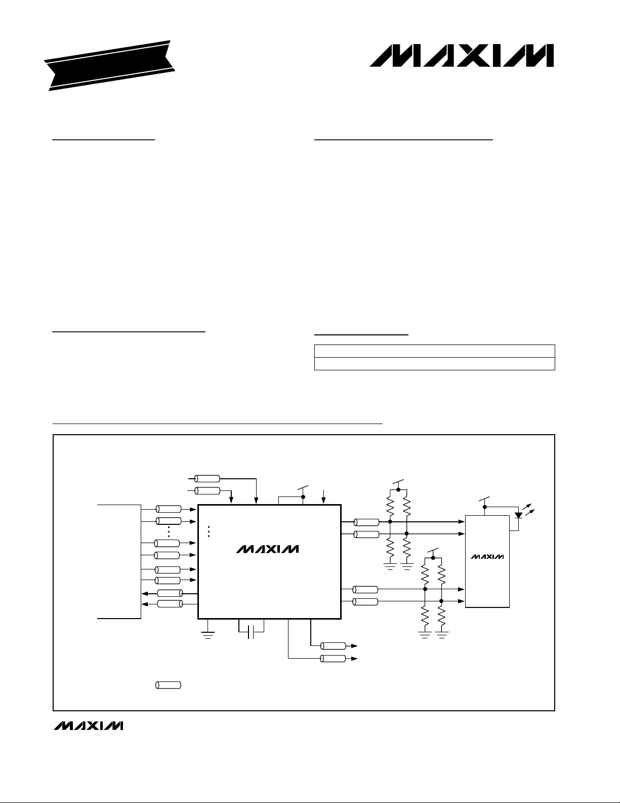
System Loopback
The MAX3890 is designed to allow system loopback testing. The loopback outputs (SLBO+, SLBO-) of the
MAX3890 may be directly connected to the loopback
inputs of a deserializer (such as the MAX3880) for system
diagnostics. To enable the SLBO outputs, apply a TTL
logic-high signal to the SOS input. Note: The same signal
that controls the SOS enable input may also be used to
control the SIS enable input on the MAX3880.
Figure 1. Functional Diagram
PDI15+
PDI15-
LVDS
16-BIT
PARALLEL
INPUT
REGISTER
MAX3890
PDI1+
PDI1-
PDI0+
PDI0-
PCLKI+
PCLKI-
RCLKI+
RCLKI-
LVDS
LVDS
LVDS
LVDS
PHASE/FREQ
PLL
DETECT
PRESCALER
FILTER
FIL+
FIL-
CLKSET
VCO
PCLKO+
DIVIDE
BY 16
LVDS
PCLKO-
SHIFT
LATCH
16-BIT
SHIFT
REGISTER
CML
PECL
PECL
SOS
SLBO+
SLBO-
SDO+
SDO-
SCLKO+
SCLKO-
Page 7

MAX3890
+3.3V, 2.5Gbps, SDH/SONET 16:1 Serializer
with Clock Synthesis and LVDS Inputs
_______________________________________________________________________________________ 7
Low-Voltage Differential-Signal
Inputs and Outputs
The MAX3890 has LVDS inputs and outputs for interfacing with high-speed digital circuitry. The LVDS
standard is based on the IEEE 1596.3 LVDS specification. This technology uses 250mV to 400mV differential low-voltage swings to achieve fast transition
times, minimized power dissipation, and noise immunity.
For proper operation, the parallel clock LVDS outputs
(PCLKO+, PCLKO-) require 100Ω differential DC termination between the inverting and noninverting outputs.
Do not terminate these outputs to ground.
The parallel data and parallel clock LVDS inputs
(PDI_+, PDI_-, PCLKI+, PCLKI-, RCLK+, RCLK-) are
internally terminated with 100Ω differential input resistance, and therefore do not require external termination.
PECL Outputs
The serial-data PECL outputs (SDO+, SDO-, SCLKO+,
SCLKO-) require 50Ω DC termination to (VCC- 2V) (see
the
Alternative PECL-Output Termination
section).
Current-Mode Logic Outputs
The system loopback outputs (SLBO+, SLBO-) of the
MAX3890 are designed using CML. The configuration
of the MAX3890 current-mode logic (CML) output circuit includes internal 50Ω back termination to V
CC
(Figure 3). These outputs are intended to drive a 50Ω
transmission line terminated with a matched load
impedance.
Figure 2. Timing Diagram
PCLKO
PCLKI
PARALLEL
INPUT DATA
(PDI_)
SERIAL
OUTPUT DATA
(SDO)
NOTE: SIGNALS SHOWN ARE DIFFERENTIAL. FOR EXAMPLE, PCLKO = (PCLKO+) - (PCLKO-).
*PDI 15 = D15; PDI14 = D14; ...PDI0 = D0.
THIS FIGURE IS NOT INTENDED TO SHOW A SPECIFIC TIMING RELATIONSHIP BETWEEN PARALLEL
INPUT DATA AND SERIAL OUTPUT DATA.
t
SU
VALID PARALLEL DATA*
t
SKEW
t
H
*D15
D14
D13
D12
D11
D10
D9D8D7D6D5D4D3D2D1
D0
Page 8

MAX3890
+3.3V, 2.5Gbps, SDH/SONET 16:1 Serializer
with Clock Synthesis and LVDS Inputs
8 _______________________________________________________________________________________
Figure 4. Alternative PECL-Output Termination
Applications Information
Alternative PECL-Output Termination
Figure 4 shows alternative PECL-output termination
methods. Use Thevenin-equivalent termination when a
(VCC- 2V) termination voltage is not available. If ACcoupling is necessary, be sure that the coupling capacitor is placed following the 50Ω or Thevenin-equivalent
DC termination.
Layout Techniques
For best performance, use good high-frequency layout
techniques. Filter voltage supplies and keep ground
connections short. Use multiple vias where possible.
Also, use controlled-impedance transmission lines to
interface with the MAX3890 clock and data inputs and
outputs.
Figure 3. Current-Mode Logic
V
CC
50Ω 50Ω
GND
OUTPUT CIRCUIT
STRUCTURE
ESD
SLBO+
SLBO-
MAX3890
SCLKO+
OR SDO+
SCLKO-
OR SDO-
MAX3890
SCLKO+
OR SDO+
SCLKO-
OR SDO-
V
CC
SLBI+
SLBI-
50Ω
INPUT CIRCUIT
+3.3V
130Ω
= 50Ω
Z
0
Z
= 50Ω
0
= 50Ω
Z
0
Z
= 50Ω
0
50Ω
130Ω
PECL
INPUTS
82Ω 82Ω
HIGHIMPEDANCE
INPUTS
50Ω 50Ω
V
- 2V
CC
Page 9

MAX3890
+3.3V, 2.5Gbps, SDH/SONET 16:1 Serializer
with Clock Synthesis and LVDS Inputs
_______________________________________________________________________________________ 9
Figure 5. Driver Output Levels
D
V
PD-
SINGLE-ENDED OUTPUT
V
PD+
- V
V
PD+
PD-
DIFFERENTIAL OUTPUT
PD+
PD-
0V (DIFF)
= 100Ω
R
L
V
V
OD
V
OH
V
ODp-p
V
OS
V
OL
= V
- V
PD+
PD-
V
|
OD|
+V
OD
0V
-V
OD
Page 10

MAX3890
+3.3V, 2.5Gbps, SDH/SONET 16:1 Serializer
with Clock Synthesis and LVDS Inputs
10 ______________________________________________________________________________________
___________________Chip Information
TRANSISTOR COUNT: 4126
SDO-
FIL+
PDI15+
TQFP-EP
TOP VIEW
PDI15-
PDI14+
PDI14-
PDI13+
PDI13-
PDI12+
PDI12-
PDI11+
PDI11-
PDI10+
PDI10-
PDI9+
PDI9-
V
CC
GND
V
CC
FIL-
RCLK-
CLKSET
V
CC
RCLK+
PCLKO+
PCLKO-
PDI0+
PDI0-
PDI1+
PDI1-
GND
PDI2-
PDI2+
PDI3-
PDI3+
PDI4-
PDI4+
PDI5-
PDI5+
PDI6-
PDI6+
PDI7-
PDI7+
PDI8-
PDI8+
GND
V
CC
SCLKO+
SCLKO-
V
CC
SOS
PCLKI-
PCLKI+
V
CC
V
CC
SDO+
V
CC
SLBO+
SLBO-
V
CC
GNDGND
GND
V
CC
5859606162 5455565763
38
39
40
41
42
43
44
45
46
47
5253
49
5051
33
34
35
36
37
48
64
2322212019 2726252418 2928 32313017
11
10
9
8
7
6
5
4
3
2
16
15
14
13
12
1
MAX3890
Pin Configuration
Page 11

MAX3890
+3.3V, 2.5Gbps, SDH/SONET 16:1 Serializer
with Clock Synthesis and LVDS Inputs
______________________________________________________________________________________ 11
Package Information
48L,TQFP.EPS
48L,TQFP.EPS
Page 12

MAX3890
+3.3V, 2.5Gbps, SDH/SONET 16:1 Serializer
with Clock Synthesis and LVDS Inputs
Maxim cannot assume responsibility for use of any circuitry other than circuitry entirely embodied in a Maxim product. No circuit patent licenses are
implied. Maxim reserves the right to change the circuitry and specifications without notice at any time.
12
____________________Maxim Integrated Products, 120 San Gabriel Drive, Sunnyvale, CA 94086 408-737-7600
© 1999 Maxim Integrated Products Printed USA is a registered trademark of Maxim Integrated Products.
Package Information (continued)
 Loading...