

Page 1
General Description
The MAX3875 is a compact, low-power clock recovery
and data retiming IC for 2.488Gbps SDH/SONET applications. The fully integrated phase-locked loop recovers a synchronous clock signal from the serial NRZ
data input, which is retimed by the recovered clock.
Differential PECL-compatible outputs are provided for
both clock and data signals, and an additional
2.488Gbps serial input is available for system loopback
diagnostic testing. The device also includes a TTLcompatible loss-of-lock (LOL) monitor.
The MAX3875 is designed for both section-regenerator
and terminal-receiver applications in OC-48/STM-16
transmission systems. Its jitter performance exceeds all
of the SONET/SDH specifications.
This device operates from a single +3.3V to +5.0V supply
over a -40°C to +85°C temperature range. The typical
power consumption is only 400mW with a +3.3V supply. It is
available in a 32-pin TQFP package, as well as in die form.
Applications
SDH/SONET Receivers and Regenerators
Add/Drop Multiplexers
Digital Cross-Connects
2.488Gbps ATM Receiver
Digital Video Transmission
SDH/SONET Test Equipment
Features
♦ Exceeds ANSI, ITU, and Bellcore SONET/SDH
Regenerator Specifications
♦ 400mW Power Dissipation (at +3.3V)
♦ Clock Jitter Generation: 0.003UI
RMS
♦ Single +3.3V or +5V Power Supply
♦ Fully Integrated Clock Recovery and Data Retiming
♦ Additional High-Speed Input Facilitates System
Loopback Diagnostic Testing
♦ Tolerates >2000 Consecutive Identical Digits
♦ Loss-of-Lock Indicator
♦ Differential PECL-Compatible Data and Clock
Outputs
For free samples & the latest literature: http://www.maxim-ic.com, or phone 1-800-998-8800.
For small orders, phone 1-800-835-8769.
MAX3875
2.5Gbps, Low-Power, +3.3V
Clock Recovery and Data Retiming IC
________________________________________________________________
Maxim Integrated Products
1
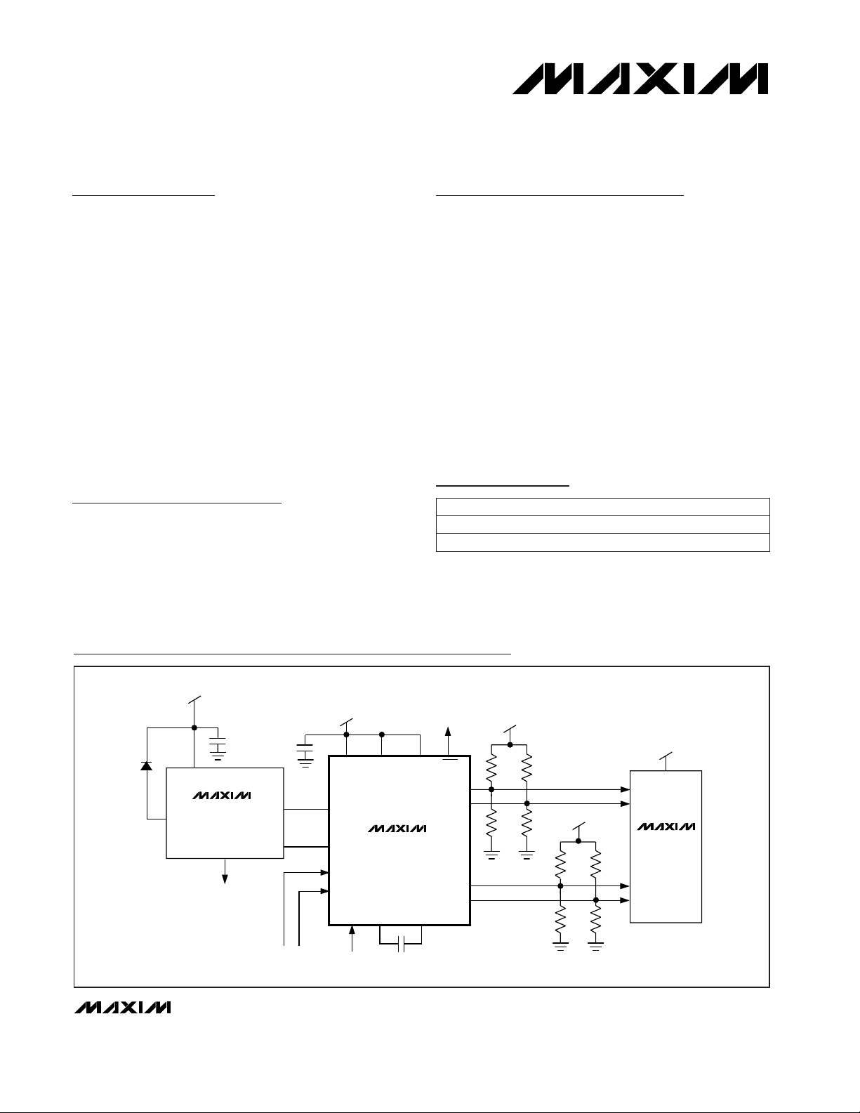
PRE/POSTAMPLIFIER
PHOTODIODE
+3.3V
SDI-
SDI+
SLBISLBI+
SDO-
SCLKO+
SCLKO-
SDO+
MAX3875
MAX3866
+3.3V
+3.3V
+3.3V
+3.3V
OUT+
OUT-
TTL
LOP
IN
LOLPHADJ-PHADJ+V
CC
V
CC
SIS FIL+ FIL-
SYSTEM
LOOPBACK
TTL
TTL
1µF
0.01µF
0.01µF
82Ω 82Ω
130Ω 130Ω
82Ω 82Ω
130Ω 130Ω
1:16
DESERIALIZER
MAX3885
Typical Application Circuit
19-4789; Rev 0; 10/98
PART
MAX3875EHJ -40°C to +85°C
TEMP. RANGE PIN-PACKAGE
32 TQFP
Ordering Information
Pin Configuration appears at end of data sheet.
MAX3875E/D -40°C to +85°C Dice*
*
Dice are designed to operate over this range, but are tested
and guaranteed at TA= +25°C only. Contact factory for
availability.
Page 2
MAX3875
2.5Gbps, Low-Power, +3.3V
Clock Recovery and Data Retiming IC
2 _______________________________________________________________________________________
ABSOLUTE MAXIMUM RATINGS
DC ELECTRICAL CHARACTERISTICS
(VCC= +3.0V to +5.5V, TA= -40°C to +85°C, unless otherwise noted. Typical values are at +3.3V and TA= +25°C.) (Note 1)
Stresses beyond those listed under “Absolute Maximum Ratings” may cause permanent damage to the device. These are stress ratings only, and functional
operation of the device at these or any other conditions beyond those indicated in the operational sections of the specifications is not implied. Exposure to
absolute maximum rating conditions for extended periods may affect device reliability.
Supply Voltage, VCC..............................................-0.5V to +7.0V
Input Voltage Levels
(SDI+, SDI-, SLBI+, SLBI-)...........(V
CC
- 0.5V) to (VCC+ 0.5V)
Input Current Levels (SDI+, SDI-, SLBI+, SLBI-)..............±10mA
PECL Output Voltage
(SDO+, SDO-, SCLKO+, SCLKO-).......................(V
CC
+ 0.5V)
PECL Output Current, (SDO+, SDO-, SCLKO+, SCLKO-).....56mA
Voltage at LOL, SIS, PHADJ+, PHADJ-,
FIL+, FIL-.................................................-0.5V to (V
CC
+ 0.5V)
Continuous Power Dissipation (T
A
= +85°C)
TQFP (derate 16.1mW/°C above +85°C)........................1.0W
Operating Temperature Range
MAX3875EHJ..................................................-40°C to +85°C
Operating Junction Temperature (die)..............-55°C to +150°C
Storage Temperature Range.............................-60°C to +160°C
Processing Temperature (die).........................................+400°C
Lead Temperature (soldering, 10sec).............................+300°C
Figure 1
Excluding PECL output termination
TA= 0°C to +85°C
TA= 0°C to +85°C
CONDITIONS
VVCC- 0.4 VCC+ 0.2V
IS
Single-Ended Input Voltage
(SDI±, SLBI±)
mVp-p50 800 V
ID
mA122 167I
CC
Supply Current
Differential Input Voltage
(SDI±, SLBI±)
V2.4 V
CC
V
OH
TTL Output High Voltage (LOL)
µA-10 +10TTL Input Current (SIS)
V0.8V
IL
TTL Input Low Voltage (SIS)
Ω45R
IN
Input Termination to V
CC
(SDI±, SLBI±)
V
VCC- 1.025 VCC- 0.88
V
OH
PECL Output High Voltage
(SDO±, SCLKO±)
V
VCC- 1.81 VCC- 1.62
V
OL
PECL Output Low Voltage
(SDO±, SCLKO±)
V2.0V
IH
TTL Input High Voltage (SIS)
UNITSMIN TYP MAXSYMBOLPARAMETER
TTL Output Low Voltage (LOL)
V
OL
0.4 V
VCC- 1.085 VCC- 0.88
VCC- 1.83 VCC- 1.555
TA = -40°C
TA = -40°C
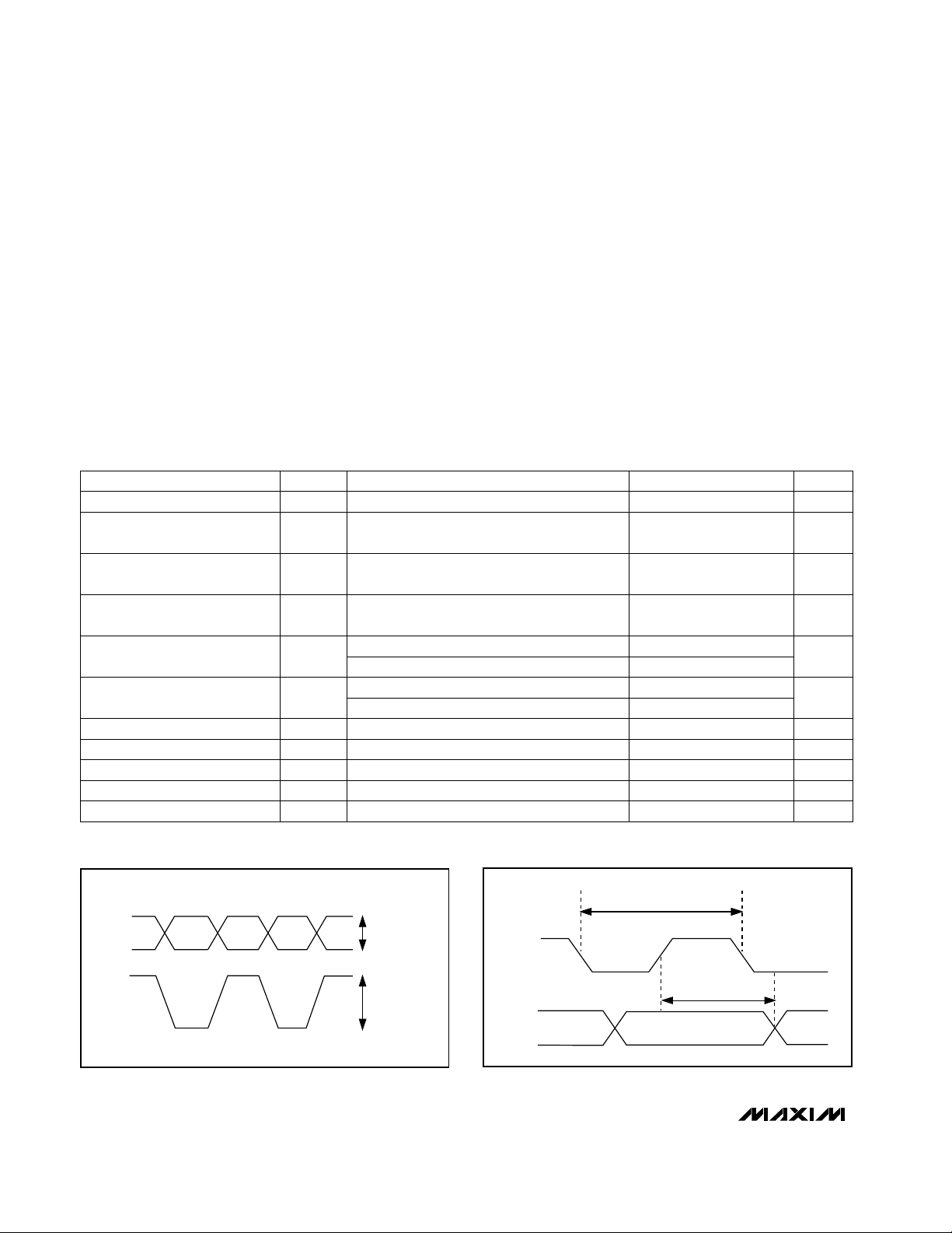
Figure 1. Input Amplitude Figure 2. Output Clock-to-Q Delay
SCLKO+
SDO
t
CK
t
CK-Q
Note 1: Dice are tested at TA= +25°C only.
SDI+
SDI-
(SDI+) -
(SDI-)
V
ID
25mV MIN
400mV MAX
50mVp-p MIN
800mVp-p MAX
Page 3
MAX3875
2.5Gbps, Low-Power, +3.3V
Clock Recovery and Data Retiming IC
_______________________________________________________________________________________ 3
AC ELECTRICAL CHARACTERISTICS
(VCC= +3.0V to +5.5V, TA= -40°C to +85°C, unless otherwise noted. Typical values are at +3.3V and TA= +25°C.) (Note 2)
Clock Output Edge Speed 20% to 80%
f ≤ 2MHz
70 ps
Figure 2
1.76 2.75
0.21 0.45
f = 100kHz
f = 10MHz (Note 3)
f = 70kHz
f = 1MHz
CONDITIONS
dB0.1J
P
Jitter Peaking
ps110 290
Gbps2.488Serial Output Clock Rate
Clock-to-Q Delay
UIp-p0.026 0.056
UI
RMS
0.003 0.006
J
GEN
Jitter Generation
MHz1.1 2.0J
BW
Jitter Transfer Bandwidth
UIp-p
1.91 3.6
Jitter Tolerance
0.41 0.67
UNITSMIN TYP MAXSYMBOLPARAMETER
Data Output Edge Speed 20% to 80% 108 ps
Tolerated Consecutive
Identical Digits
2000
Bits
100kHz to 2.5GHz -17
2.5GHz to 4.0GHz -15
Jitter BW = 12kHz to 20MHz
Note 2: AC characteristics are guaranteed by design and characterization.
Note 3: See
Typical Operating Characteristics
for worst-case distribution.
Input Return Loss
(SDI±, SLBI±)
dB
Typical Operating Characteristics
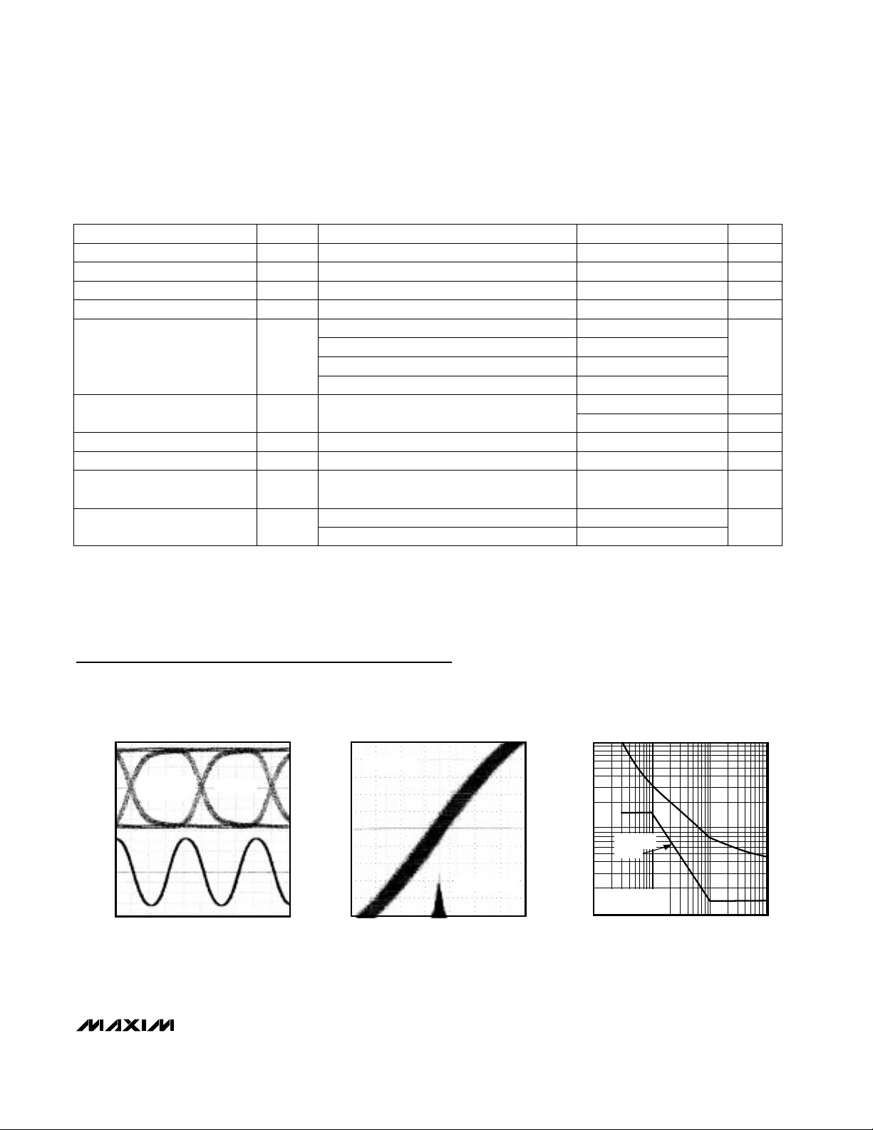
(VCC= +3.3V, TA = +25°C, unless otherwise noted.)
RECOVERED CLOCK JITTER
MAX3875 toc02
10ps/div
PRBS = 2
15
- 1
RMS∆ = 1.2ps
0.1
10k 10M100k 1M
JITTER TOLERANCE
1
10
MAX3875 toc03
JITTER FREQUENCY (Hz)
INPUT JITTER (UIp-p)
PRBS = 223 - 1
50mVp-p INPUT
BELLCORE
MASK
RECOVERED DATA AND CLOCK
(DIFFERENTIAL OUTPUT)
MAX3875 toc01
100ps/div
CLOCK
DATA
2
23
- 1 PATTERN
V
IN
= 20mV
P-P
TA = +85°C
Page 4
MAX3875
2.5Gbps, Low-Power, +3.3V
Clock Recovery and Data Retiming IC
4 _______________________________________________________________________________________
10
-10
10
-7
10
-8
10
-5
10
-6
10
-4
10
-3
6.0 6.3 6.46.1 6.2 6.5 6.6
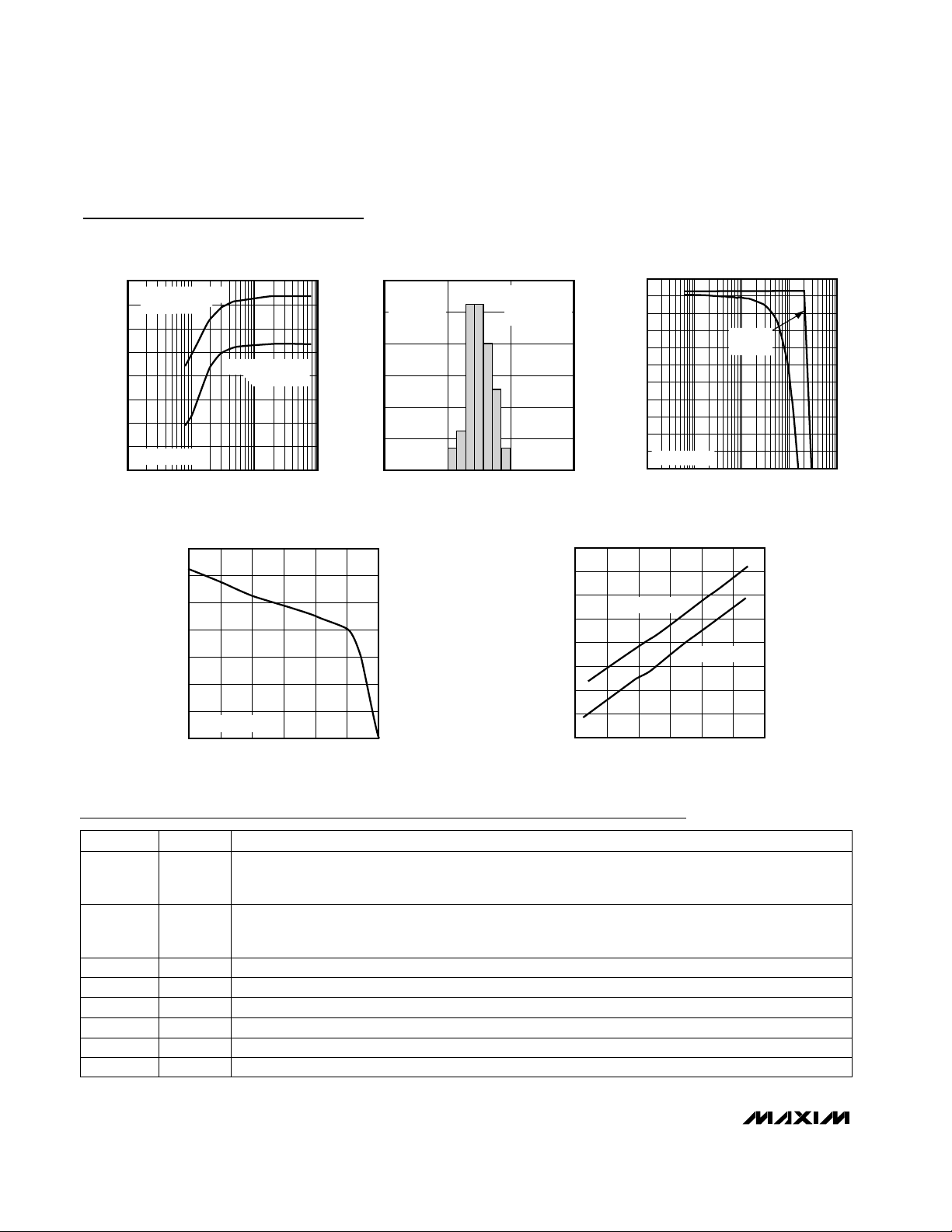
BIT ERROR RATE vs. INPUT VOLTAGE
MAX3875toc06
INPUT VOLTAGE (mVp-p)
BIT ERROR RATE
PRBS = 223 - 1
10
-9
105
120
125
115
110
135
130
140
145
-50 25 50-25 0 75 100
SUPPLY CURRENT
vs. TEMPERATURE
MAX3875toc07
AMBIENT TEMPERATURE (°C)
SUPPLY CURRENT (mA)
VCC = +3.3V
VCC = +5.0V
NAME FUNCTION
1, 2, 8, 9,
10, 16, 26,
29, 32
GND Supply Ground
3, 6, 11,
14, 15, 17,
20, 21, 24
V
CC
Positive Supply Voltage
PIN
4 SDI+ Positive Data Input. 2.488Gbps serial data stream.
5 SDI- Negative Data Input. 2.488Gbps serial data stream.
13 SLBI- Negative System Loopback Input. 2.488Gbps serial data stream.
12 SLBI+ Positive System Loopback Input. 2.488Gbps serial data stream.
7 SIS Signal Input Selection, TTL. Low for normal data input. High for system loopback input.
Pin Description
0.8
0
0.1
0.2
1 100 1000
JITTER TOLERANCE vs. INPUT VOLTAGE
0.3
0.4
0.5
0.6
0.7
MAX3875toc04
INPUT VOLTAGE (mVp-p)
JITTER TOLERANCE (UIp-p)
10
JITTER FREQUENCY
= 1MHz
JITTER FREQUENCY
= 5MHz
PRBS = 223 - 1
0.3
-3.0
-2.7
1k 100k 1M10k 10M
JITTER TRANSFER
-2.4
-2.1
MAX3875 toc05
JITTER FREQUENCY (Hz)
-1.8
-1.5
-1.2
-0.9
JITTER TRANSFER (dB)
-0.6
-0.3
0
PRBS = 223 - 1
BELLCORE
MASK
0
20
15
10
5
25
30
0.20 0.480.34 0.62
DISTRIBUTION OF JITTER TOLERANCE
MAX3875toc05a
JITTER TOLERANCE (UIp-p)
PERCENT OF UNITS (%)
MEAN = 0.41
σ = 0.028
f
JITTER
= 10MHz
V
CC
= +3.0V
T
A
= -40°C
Typical Operating Characteristics (continued)
(VCC= +3.3V, TA = +25°C, unless otherwise noted.)
18
SCLKO- Negative Serial Clock Output, PECL, 2.488GHz. SDO- is clocked out on the falling edge of SCLKO-.
Page 5

MAX3875
2.5Gbps, Low-Power, +3.3V
Clock Recovery and Data Retiming IC
_______________________________________________________________________________________ 5
SDI+
SDI-
SLBI+
SLBI-
SCLKO-
SCLKO+
SDO+
SDO-
PHASE &
FREQUENCY
DETECTOR
PHADJ- FIL+ FIL-
LOOP
FILTER
MAX3875
LOL
PHADJ+SISSIS
MUX
AMP
AMP
CK
D Q
VCO
I
Q
PECL
PECL
TTL
Figure 3. Functional Diagram
NAME FUNCTIONPIN
27 PHADJ- Negative Phase-Adjust Input. Used to optimally align internal PLL phase. Connect to VCCif not used.
25
LOL
Loss-of-Lock Output, TTL, PLL loss-of-lock monitor, active low (internal 10kΩ pull-up resistor)
23 SDO+ Positive Data Output, PECL compatible, 2.488Gbps
22 SDO- Negative Data Output, PECL compatible, 2.488Gbps
19 SCLKO+ Positive Serial Clock Output, PECL, 2.488GHz. SDO+ is clocked out on the rising edge of SCLKO+.
28
PHADJ+
Positive Phase-Adjust Input. Used to optimally align internal PLL phase. Connect to VCCif not used.
30 FIL- Negative Filter Input. PLL loop filter connection. Connect a 1.0µF capacitor between FIL+ and FIL-.
31 FIL+ Positive Filter Input. PLL loop filter connection. Connect a 1.0µF capacitor between FIL+ and FIL-.
Pin Description (continued)
Detailed Description
The MAX3875 consists of a fully integrated phaselocked loop (PLL), input amplifier, data retiming block,
and PECL output buffer (Figure 3). The PLL consists of
a phase/frequency detector (PFD), a loop filter, and a
voltage-controlled oscillator (VCO).
This device is designed to deliver the best combination
of jitter performance and power dissipation by using a
fully differential signal architecture and low-noise
design techniques.
Input Amplifier
Input amplifiers are implemented for both the main data
and system loopback inputs. These amplifiers accept a
differential input amplitude from 50mVp-p up to
800mVp-p. The bit error rate is better than 1
· 10
-10
for
input signals as small as 10mVp-p, although the jitter
tolerance performance will be degraded. For interfacing
with PECL signal levels, see
Applications Information
.
Phase Detector
The phase detector incorporated in the MAX3875 produces a voltage proportional to the phase difference
between the incoming data and the internal clock.
Because of its feedback nature, the PLL drives the
error voltage to zero, aligning the recovered clock to
the center of the incoming data eye for retiming. The
external phase adjust pins (PHADJ+, PHADJ-) allow the
user to vary the internal phase alignment.
Page 6

Frequency Detector
The digital frequency detector (FD) aids frequency
acquisition during start-up conditions. The frequency
difference between the received data and the VCO
clock is derived by sampling the in-phase and quadrature VCO outputs on both edges of the data input signal. Depending on the polarity of the frequency
difference, the FD drives the VCO until the frequency
difference is reduced to zero. Once frequency acquisition is complete, the FD returns to a neutral state. False
locking is completely eliminated by this digital frequency detector.
Loop Filter and VCO
The phase detector and frequency detector outputs are
summed into the loop filter. An external capacitor, CF,
is required to set the PLL damping ratio. Refer to
Design Procedure
for guidelines on selecting this
capacitor.
The loop filter output controls the on-chip LC VCO run-
ning at 2.488GHz. The VCO provides low phase noise
and is trimmed to the correct frequency. Clock jitter
generation is typically 1.2ps
RMS
within a jitter band-
width of 12kHz to 20MHz.
Loss-of-Lock Monitor
A loss-of-lock (LOL) monitor is incorporated in the
MAX3875 frequency detector. A loss-of-lock condition
is signaled immediately with a TTL low. When the PLL is
frequency locked, LOL switches to TTL high in approximately 800ns.
Note that the LOL monitor is only valid when a data
stream is present on the inputs to the MAX3875. As a
result, LOL does not detect a loss-of-power condition
resulting from a loss of the incoming signal.
Design Procedure
Setting the Loop Filter
The MAX3875 is designed for both regenerator and
receiver applications. Its fully integrated PLL is a classic second-order feedback system, with a loop bandwidth (fL) fixed at 1.1MHz. The external capacitor, CF,
can be adjusted to set the loop damping. Figures 4 and
5 show the open-loop and closed-loop transfer functions.
The PLL zero frequency, fZ, is a function of external
capacitor CF, and can be approximated according to:
For an overdamped system (f
Z/fL
) < 0.25, the jitter peaking (MP) of a second-order system can be approximated by:
For example, using CF= 0.1µF results in a jitter peaking
of 0.2dB. Reducing CFbelow 0.01µF may result in PLL
instability. The recommended value for CF= 1.0µF to
guarantee a maximum jitter peaking of less than 0.1dB.
CFmust be a low TC, high-quality capacitor of type
X7R or better.
M
f
f
P
Z
L
=
20log 1+
f
60 C
z
F
=
( )
1
2π
MAX3875
2.5Gbps, Low-Power, +3.3V
Clock Recovery and Data Retiming IC
6 _______________________________________________________________________________________
CF = 1.0µF
f
Z
= 2.6kHz
C
F
= 0.1µF
f
Z
= 26kHz
H
O
(j2πf) (dB)
OPEN-LOOP GAIN
1000
f (kHz)
100
101
Figure 4. Open-Loop Transfer Function
CF = 1.0µF
H(j2πf) (dB)
1000
100
10
1
f (kHz)
-3
0
CLOSED-LOOP GAIN
CF = 0.1µF
Figure 5. Closed-Loop Transfer Function
Page 7

Input and Output Terminations
The MAX3875’s digital outputs (SDO+, SDO-, SCLKO+,
SCLKO-) are designed to interface with PECL signal
levels. It is important to bias these ports appropriately.
A circuit that provides a Thevenin equivalent of 50Ω to
VCC- 2V can be used with fixed impedance transmission lines for proper termination. To ensure best performance, the differential outputs must have balanced
loads. The input termination can be driven differentially,
or can be driven single-ended by externally biasing
SDI- or SLBI- to the center of the voltage swing.
Jitter Tolerance and Input
Sensitivity Trade-Offs
When the received data amplitude is higher than
50mVp-p, the MAX3875 provides a typical jitter tolerance of 0.45UI at jitter frequencies greater than 10MHz.
The SDH/SONET jitter tolerance specification is 0.15UI,
leaving a jitter allowance of 0.3UI for receiver preamplifier and postamplifier design.
The BER is better than 1 · 10
-10
for input signals greater
than 10mVp-p. At 10mVp-p, jitter tolerance will be
degraded, but will still be above the SDH/SONET
requirement. The user can make a trade-off between jitter tolerance and input sensitivity according to the specific application. Refer to the
Typical Operating
Characteristics
for Jitter Tolerance and BER vs. Input
Amplitude graphs.
Applications Information
Consecutive Identical Digits (CID)
The MAX3875 has a low phase and frequency drift in
the absence of data transitions. As a result, long runs of
consecutive zeros and ones can be tolerated while
maintaining a BER of 1 · 10
-10
. The CID tolerance is
tested using a 2
13
- 1 PRBS, substituting a long run of
zeros to simulate the worst case. A CID tolerance of
2000 bits is typical.
Phase Adjust
The internal clock is aligned to the center of the data
eye. For specific applications this sampling position
can be shifted using the PHADJ inputs to optimize BER
performance. The PHADJ inputs operate with differential input voltages up to ±1.5V. A simple resistor-divider
with a bypass capacitor is sufficient to set these levels.
When the PHADJ inputs are not used, they should be
tied directly to VCC.
System Loopback
The MAX3875 is designed to allow system loopback
testing. The user can connect a serializer output in a
transceiver directly to the SLBI+ and SLBI- inputs of the
MAX3875 for system diagnostics. To select the SLBI±
inputs, apply a TTL logic high to the SIS pin.
PECL Input Levels
When interfacing with differential PECL input levels, it is
important to attenuate the signal while still maintaining
50Ω termination (Figure 6). AC coupling is also
required to maintain the input common-mode level.
Layout
The MAX3875’s performance can be significantly
affected by circuit board layout and design. Use good
high-frequency design techniques, including minimizing ground inductance and using fixed-impedance
transmission lines on the data and clock signals.
Power-supply decoupling should be placed as close to
VCCas possible. Take care to isolate the input from the
output signals to reduce feedthrough.
MAX3875
2.5Gbps, Low-Power, +3.3V
Clock Recovery and Data Retiming IC
_______________________________________________________________________________________ 7
MAX3875
50Ω
50Ω
V
CC
100Ω
PECL
LEVELS
SDI+
25Ω
25Ω
0.1µF
0.1µF
SDI-
Figure 6. PECL Input Interface
Page 8
MAX3875
2.5Gbps, Low-Power, +3.3V
Clock Recovery and Data Retiming IC
Maxim cannot assume responsibility for use of any circuitry other than circuitry entirely embodied in a Maxim product. No circuit patent licenses are
implied. Maxim reserves the right to change the circuitry and specifications without notice at any time.
8
_____________________Maxim Integrated Products, 120 San Gabriel Drive, Sunnyvale, CA 94086 408-737-7600
© 1998 Maxim Integrated Products Printed USA is a registered trademark of Maxim Integrated Products.
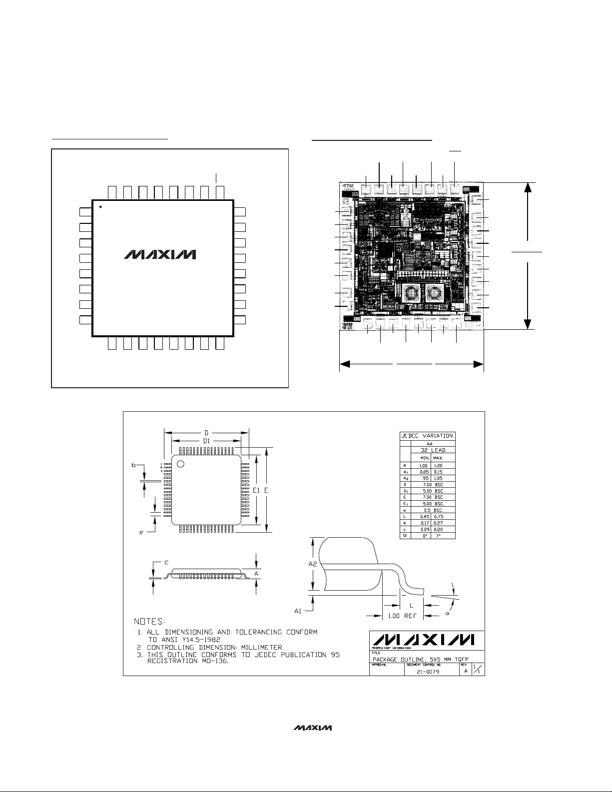
________________________________________________________Package Information
Pin Configuration
MAX3875
TQFP
TOP VIEW
32 28
293031
25
26
27
FIL+
FIL-
GND
PHADJ+
GND
PHADJ-
GND
LOL
10
13
15
14
1611 12
9
GND
V
CC
GND
SLBI-
SLBI+
V
CC
V
CC
GND
17
18
19
20
21
22
23
SDO+
24 V
CC
SDOV
CC
V
CC
SCLKO+
SCLKOV
CC
2
3
4
5
6
7
8GND
SIS
V
CC
SDI-
SDI+
V
CC
GND
1GND
Chip Topography
GND
V
CC
SLBI+
SLBI-
V
CC
N.C.
V
CC
N.C.
0.072"
(1.828mm)
0.071"
(1.803mm)
V
CC
SDO+
SDO-
V
CC
V
CC
SCLKO+
SCLKOV
CC
GND
GND
GND
V
CC
SDI+
SDI-
V
CC
SIS
GND
GND
FIL+
FIL-
GND
PHADJ+
PHADJ-
GND
LOL
TRANSISTOR COUNT: 1515
32TQFP.EPS
 Loading...