

Page 1
For free samples & the latest literature: http://www.maxim-ic.com, or phone 1-800-998-8800.
For small orders, phone 1-800-835-8769.
General Description
The MAX3866 combined transimpedance preamplifier
and limiting postamplifier is intended for application in
SDH/SONET systems operating at 2.488Gbps. It operates from a single +3.3V or +5V supply and provides a
differential output signal. The differential outputs are
each 50Ω reverse terminated (100Ω differential termination) for low-noise and high-speed signal performance.
The small-signal bandwidth and noise performance is
specified for a source capacitance of 0.5pF. When the
MAX3866 is used with the PIN photodetector, sensitivities better than -22dBm can be achieved. The
MAX3866 is equipped with a programmable TTL lossof-power (LOP) output.
Applications
SDH/SONET Transmission Systems
PIN/Preamplifier Receivers
2.488Gbps ATM Receivers
Regenerators for SDH/SONET
Features
♦ Input Sensitivities Better than -22dBm (7.8µAp-p)
♦ Overdrive Capability Better than +1.4dBm
(2.5mAp-p)
♦ Single +3.3V or +5V Supply
♦ 165mW Power Dissipation (at 3.3V)
♦ 1.8GHz Analog Input Bandwidth
♦ Programmable Loss-of-Power Indicator
♦ 100Ω Differential Output
MAX3866
2.5Gbps, +3.3V Combined
Transimpedance/Limiting Amplifier
________________________________________________________________
Maxim Integrated Products
1
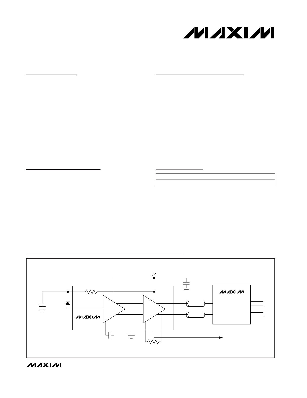
Zo = 50Ω
Zo = 50Ω
+3.3V
PHOTODIODE
CHF+ PDCCHF- INV
C
HF
R
PD
FIL
IN+
MAX3866
LIMITING
POSTAMP
PREAMP
LOP
OUT+
VCCS
VCCD
OUT-
CLOCK AND DATA
RECOVERY
MAX3875
200Ω
Typical Application Circuit
19-1433; Rev 1; 3/99
PART
MAX3866E/D (see Note)
TEMP. RANGE PIN-PACKAGE
Dice
Note: Dice are designed to operate over a -40°C to +120°C
junction temperature (T
j
) range, but are tested and guaranteed
at TA= +25°C.
Pad Configuration appears at end of data sheet.
Ordering Information
Page 2
MAX3866
2.5Gbps, +3.3V Combined
Transimpedance/Limiting Amplifier
2 _______________________________________________________________________________________
ABSOLUTE MAXIMUM RATINGS
DC ELECTRICAL CHARACTERISTICS
(VCCD = VCCS = +3.3V ±5% or VCCD = +5.0V ±10%, VCCS = open, Tj= -40°C to +120°C, unless otherwise noted. Typical values
are at +3.3V and T
j
= +25°C.)
Stresses beyond those listed under “Absolute Maximum Ratings” may cause permanent damage to the device. These are stress ratings only, and functional
operation of the device at these or any other conditions beyond those indicated in the operational sections of the specifications is not implied. Exposure to
absolute maximum rating conditions for extended periods may affect device reliability.
Note 1: CIN= total capacitance on IN.
Note 2: AC parameters are guaranteed by design and characterization.
Note 3: See
Typical Operating Characteristics
for worst-case distribution.
Note 4: Hysteresis = 20 log (V
DEASSERT
/ V
ASSERT
).
Note 5: I
IN
= 2.5mA.
Note 6: PWD = [(2 · Pulse Width) - Period] / 2.
Note 7: External load not required for normal operation.
VCCD Voltage .......................................................-0.5V to +7.0V
VCCS Voltage...............0 ≤ VCCS ≤ VCCD and if VCCD ≥ 3.13V
then 3.13V ≤ VCCS ≤ VCCD
CHF+, CHF-, FIL, INV, LOP Voltage.......-0.5V to (VCCD + 0.5V)
IN-, IN+ Voltage.....................................................-0.5V to +1.0V
CPD+, CPD- Voltage................(VCCD - 1.6V) to (VCCD + 0.5V)
OUT+, OUT- Voltage................(VCCD - 1.1V) to (VCCD + 0.5V)
IN Current.......................................................................0 to 3mA
PDC Current..................................................................-1mA to 0
Operating Junction Temperature Range (T
j
).....-55°C to +125°C
Storage Temperature Range.............................-60°C to +160°C
Processing Temperature (Die).........................................+400°C
Load = 4.7kΩ to V
CCD
(Note 7)
Load = 4.7kΩ to V
CCD
(Note 7)
RL= 100Ω (differential), IIN≥ 7µAp-p
RL= 100Ω (differential)
CONDITIONS
Ω90 105 120Z
OUT
Differential Output Impedance
V0.84 0.95V
IN
mA50 73I
VCC
Supply Current
Input Bias Voltage
VV
CCD
- 0.1 V
CCD
V
OH
LOP Output High Voltage
V0.4V
OL
LOP Output Low Voltage
mVp-p100 145V
OD
Differential Output Voltage Swing
VV
CCD
- 0.12V
CM
Output Common-Mode Voltage
UNITSMIN TYP MAXSYMBOLPARAMETER
(Notes 5, 6)
20% to 80% (Note 5)
RPD= 510Ω
RPD= 510Ω
CIN= 0.5pF, Tj= +120°C
2.5Gbps, 223- 1 PRBS, BER ≤ 10
-10
,
CIN= 0.5pF, Tj= +120°C
Electrical (Note 4), low LOP assert,
RPD= 510Ω
f ≤ 2MHz, 100mVp-p
CONDITIONS
ps21 80PWDPulse-Width Distortion
ps50 70tr, t
f
Output Edge Speed
µA8.0LOP Deassert Level
µA0.9LOP Assert Level
dB3LOP Hysteresis
dB25 30PSRRPower-Supply Rejection Ratio
kHz100f
L
Low-Frequency Cutoff
nA433 566N
IN
Input-Referred RMS Noise
µAp-p7.8 (Note 3)I
IN
Input Sensitivity
GHz1.8BWSmall-Signal Bandwidth
UNITSMIN TYP MAXSYMBOLPARAMETER
AC ELECTRICAL CHARACTERISTICS
(VCCD = VCCS = +3.3V ±5% or VCCD = +5.0V ±10%, VCCS = open, Tj= -40°C to +120°C, unless otherwise noted. Typical values
are at +3.3V and T
j
= +25°C.) (Notes 1, 2)
Page 3
MAX3866
2.5Gbps, +3.3V Combined
Transimpedance/Limiting Amplifier
_______________________________________________________________________________________
3
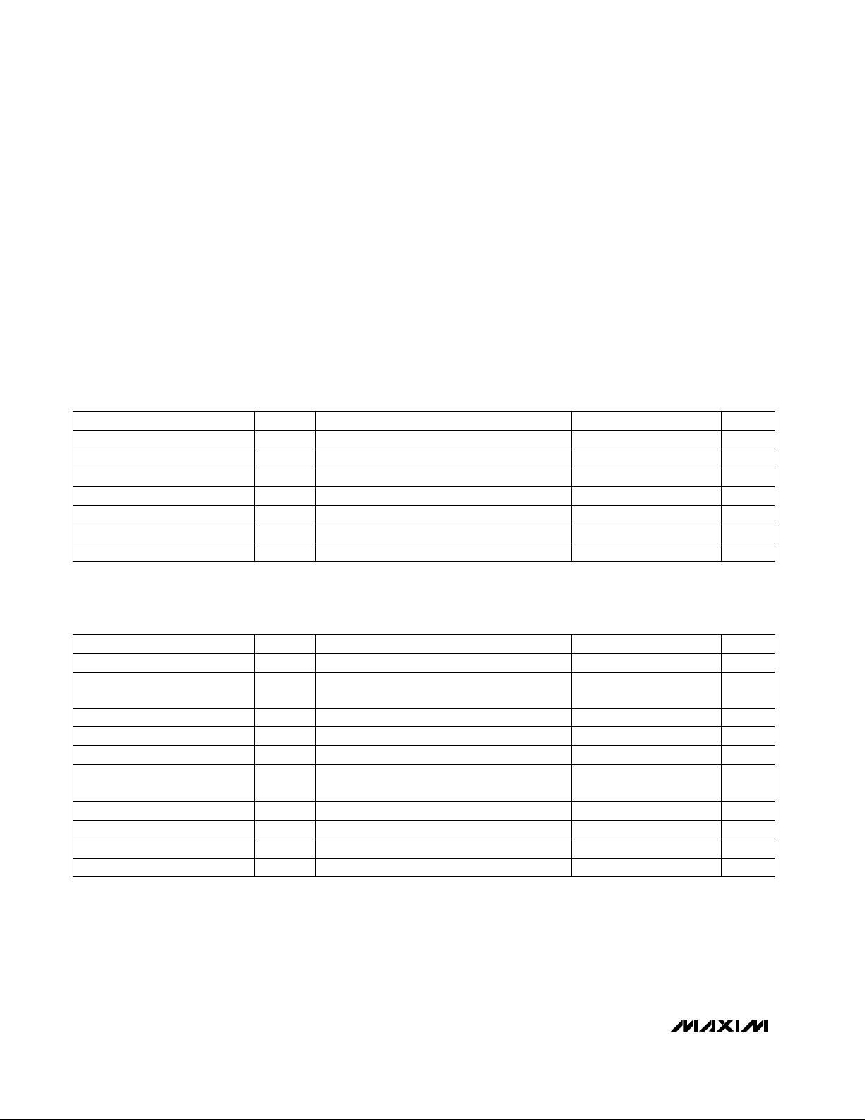
90
0
10 100
LOP ASSERT/DEASSERT
vs. R
PD
50
40
30
20
10
MAX3866 TOC01
RPD (Ω)
ASSERT/DEASSERT (µA)
60
70
80
ASSERT
DEASSERT
0
4
2
8
6
10
12
14
16
-60 -20 0-40 20 40 60 80 100
PULSE-WIDTH DISTORTION
vs. TEMPERATURE
MAX3866 TOC02
TEMPERATURE (¡C)
PWD (ps)
IN+ = 100µA
3.00
3.35
3.30
3.25
3.20
3.15
3.10
3.05
3.45
3.40
3.50
-50 -20 0-30 20 40 60 80 100
OUTPUT COMMON-MODE VOLTAGE
vs. TEMPERATURE
MAX3866 toc03
TEMPERATURE (°C)
COMMON-MODE VOLTAGE (V)
OUT+
OUT-
100
105
115
110
125
120
130
135
145
140
150
-60 -40 -20 0 20 40 60 80 100
DIFFERENTIAL OUTPUT VOLTAGE
vs. TEMPERATURE
MAX3866 TOC04
TEMPERATURE (°C)
DIFFERENTIAL OUTPUT VOLTAGE (mVp-p)
1k 10k
-20
-15
-10
-5
0
10
5
15
20
1 10 100
PULSE-WIDTH DISTORTION
vs. INPUT CURRENT
MAX3866 TOC07
INPUT CURRENT (µA)
PWD (ps)
30
40
60
50
70
80
90
100
-50 -10 10-30 30 50 70 90
SUPPLY CURRENT
vs. TEMPERATURE
MAX3866 TOC05
TEMPERATURE (°C)
SUPPLY CURRENT (mA)
3.14V
3.47V
1k 10k
100
105
110
115
120
130
125
135
140
1 10 100
OUTPUT VOLTAGE vs. INPUT CURRENT
MAX3866 TOC06
INPUT CURRENT (µA)
OUTPUT VOLTAGE (mVp-p)
ELECTRICAL EYE DIAGRAM
MAX3866 TOC08
50ps
INPUT = 8µAp-p, 2.5Gbps,
2
23
-1PRBS
R
L
= 100Ω DIFFERENTIAL
20mV/
div
ELECTRICAL EYE DIAGRAM
MAX3866 TOC09
50ps
20mV/
div
INPUT = 2.5mAp-p, 2.5Gbps,
2
23
-1PRBS
R
L
= 100Ω DIFFERENTIAL
Typical Operating Characteristics
(V
CCD
= V
CCS
= +3.3V, TA = +25°C, unless otherwise noted.)
Page 4
MAX3866
2.5Gbps, +3.3V Combined
Transimpedance/Limiting Amplifier
4 _______________________________________________________________________________________
Typical Operating Characteristics (continued)
(V
CCD
= V
CCS
= +3.3V, TA = +25°C, unless otherwise noted.)
99
98
97
89
0.01 1 10
100
0.1
1000
SMALL-SIGNAL IMPEDANCE
vs. FREQUENCY
91
90
MAX3866 toc10
FREQUENCY (MHz)
TRANSIMPEDANCE
(20log (V
OUT
p-p/IN+))
93
96
95
94
92
0
10
5
20
15
25
30
7.717.28 8.14 8.57
DISTRIBUTION OF ELECTRICAL
SENSITIVITY (WORST CASE)
MAX3866 toc11
ELECTRICAL SENSITIVITY (µAp-p)
PERCENT OF UNITS (%)
VCC = +3.14V TO +5.5V
T
j
= +120°C
FUNCTION
VCCS
Positive Supply Voltage of Input Stage. Apply +3.3V if VCCD = +3.3V. If VCCD > +3.47V, disconnect from supply and decouple to GND.
CHF+
External Filter Capacitor. A capacitor connected between CHF+ and CHF- is used for setting the low-frequency
cutoff.
PAD NAME
CHF-
External Filter Capacitor. A capacitor connected between CHF+ and CHF- is used for setting the low-frequency
cutoff.
FIL On-Chip Resistor for Filtering Photodiode Supply Voltage (connected to VCCD on chip)
PDC
The voltage at this node programs the gain of the power detector. Connect a resistor between PDC and INV to
adjust the LOP threshold.
IN- No Connect
IN+ Signal Input
GND Electrical Ground
OUT+ Noninverted Data-Signal Output
OUT- Inverted Data-Signal Output
CPD+
Filter Node for Power Detector. A capacitor connected between CPD+ and CPD- will provide additional filtering
to the rectifier output within the power detector.
CPD-
Filter Node for Power Detector. A capacitor connected between CPD+ and CPD- will provide additional filtering
to the rectifier output within the power detector.
INV
Used for programming the gain of the power detector. Connect a resistor between PDC and INV to adjust the
LOP threshold.
Pad Description
VCCD Power-Supply Voltage
LOP TTL Output, Loss-of-Power, active high
Page 5

MAX3866
2.5Gbps, +3.3V Combined
Transimpedance/Limiting Amplifier
_______________________________________________________________________________________ 5
MAX3866
OUT+
LOP
100nF
10nF
3.3V
100nF
C
HF
100nF
OUT-
OUT+
OUT-
CPD+
CPD-
CHF- CHF+
3.3V OPERATION
5.0V OPERATION
INV
PDC
VCCD
VCCS
IN+
FIL
INGND
MAX3866
OUT+
LOP
100nF
5.0V
100nF
C
HF
100nF
R
PD
*
510Ω
R
PD
*
510Ω
* NOTE: IF LOP OPERATION IS NOT DESIRED, R
PD
= 0Ω
OUT-
OUT+
OUT-
CPD+
CPD-
CHF- CHF+
INV
PDC
VCCD
VCCS
IN+
FIL
INGND
Typical Operating Circuits
Circuit Description
Data Path
The combined preamplifier and limiting postamplifier
(Figure 1) accepts an input current from a photodiode
attached to the input pad IN+. The transimpedance
input amplifier stage converts the input current to an
output voltage with a typical transimpedance of 1.4kΩ.
The second stage of the data path is an active highpass filter. This filter converts the single-ended input
signal to a differential signal, eliminating the DC component and adding approximately 16dB of gain. The
output of the highpass filter drives the power detector
and limiting amplifier circuitry.
The limiting amplifier circuit is the third stage of the
data signal path. It amplifies and limits the differential
input signal. The output stage is a differential pair with
internal 50Ω load resistors. The limited output voltage is
typically 145mVp-p.
Power Detector
The power detect circuit consists of an adjustable-gain
amplifier and combined rectifier with a lowpass filter.
The adjustable-gain amplifier is controlled by an op amp.
The gain is adjusted by means of an external resistor
connected between the PDC and INV pins.
The output voltage of the adjustable gain amplifier
drives the combined rectifier and lowpass filter circuitry. The resulting DC voltage is fed to a Schmitt trigger,
which generates a high-level output signal if the DC
input signal is below the LOP assert level, thus causing
an LOP condition on the LOP output.
Design Procedure
Power Supply
The complete amplifier is supplied by a single supply
voltage, V
CCD
. For operation at 3.3V, the supply volt-
age is applied at both the VCCD and VCCS pins (see
Typical Operating Circuit
). For operation at 5.0V, the
voltage is only applied at VCCD. In this case, VCCS is
on-chip controlled to approximately 3.2V. In the 5.0V
configuration, an external 10nF grounded capacitor is
required at the VCCS pin.
External Filter Capacitor C
HF
The value of CHFaffects the maximum speed at which
the compensation loop adjusts the input offset current.
CHFshould be chosen between 10nF and 100nF. The
loop should be as slow as possible to reduce patterndependent jitter. Maxim recommends a value of CHF=
100nF.
Page 6

External Filter Capacitor C
PD
The LF cutoff of the power detector can be reduced by
adding external capacitance across the CPD pins. This
capacitor is only needed when this circuit is operated
at lower data rates and lower edge speeds. In this way,
the remaining ripple of power detector output voltage is
reduced.
Loss-of-Power Threshold
If the LOP function is desired, Maxim recommends R
PD
= 510Ω. If the LOP function is not desired, RPD= 0Ω
(shorted). See Figure 2 for LOP definitions. If desired,
the LOP threshold can be adjusted (see Assert/
Deassert vs. RPDin the
Typical Operating Charac-
teristics.
MAX3866
2.5Gbps, +3.3V Combined
Transimpedance/Limiting Amplifier
6 _______________________________________________________________________________________
MAX. DEASSERT
INPUT CURRENT
DEASSERT
ASSERT
MIN. ASSERT
HYSTERESIS > 3dB
Figure 2. Loss-of-Power Definitions with RPD= 510
Ω
CHF+
IN
VCCS
VCCD
GND
ICC
R
F
TIA LIM
DATA SIGNAL PATH
ADJ
RECTIFIER
RMS DETECTOR
OP AMP
OUT
OUT+
OUT-
LOP
HPF
VREF
VOLTAGE
REGULATOR
CHF-
INV
PDC
R
PD
CPD+ CPD-
MAX3866
FIL
Figure 1. Functional Diagram of the Combined Preamplifier and Limiting Postamplifier
Page 7

MAX3866
2.5Gbps, +3.3V Combined
Transimpedance/Limiting Amplifier
_______________________________________________________________________________________ 7
Internal Input/Output Schematics
Figure 3. OUT Pads Figure 4. IN Pads
Figure 5. FIL Pads
Figure 6. CHF Pads
VCCD
200Ω
GND
FIL
ESD
STRUCTURE
VCCD
50Ω 50Ω
OUT+
OUT-
ESD
STRUCTURE
GND
IN+
ESD
STRUCTURE
VCCD
VCCS
IN-
ESD
STRUCTURE
GND
CHF-CHF+
ESD
STRUCTURES
GND
Page 8

MAX3866
2.5Gbps, +3.3V Combined
Transimpedance/Limiting Amplifier
8 _______________________________________________________________________________________
Internal Input/Output Schematics (continued)
VCCD
10k
LOP
GND
ESD
STRUCTURE
Figure 8. PDC Pad
Figure 10. CPD Pad
Figure 9. LOP Pad
VCCD
INV
GND
ESD
STRUCTURE
Figure 7. INV Pad
PDC
VCCD
ESD
STRUCTURE
GND
VCCD
GND
CPD+ CPD-
ESD
STRUCTURES
Page 9

Applications Information
Converting Average Optical Power
to Signal Amplitude
Many of the MAX3866’s specifications relate to input
signal amplitude. When working with fiber optic
receivers, the input is usually expressed in terms of
average optical power and extinction ratio. The relations given in Table 1 are helpful for converting optical
power to input signal when designing with the
MAX3866.
In an optical receiver, the input current to the transimpedance amplifier can be found by multiplying the
power relationships in Table 1 with the photodiode
responsivity.
Wire Bonding
Make corrections to the die with gold wire only, using
ball bonding techniques. Die pad size is 4mils (100µm)
square and die thickness is 12mils (~300µm).
Layout Techniques
The MAX3866’s performance can be greatly affected
by circuit board layout and design. Use good high-frequency design techniques, including minimizing
ground inductances and using fixed-impedance transmission lines on all data signals.
MAX3866
2.5Gbps, +3.3V Combined
Transimpedance/Limiting Amplifier
_______________________________________________________________________________________ 9
PARAMETER SYMBOL RELATION
Average
Power
P
AVE
P
AVE
= (P0 + P1) / 2
Extinction
Ratio
r
e
re= P1 / P0
Optical Power
of a “1”
P1
Optical Power
of a “0”
P0 P0 = 2P
AVE
/ (re+1)
Signal
Amplitude
P
IN
Table 1. Optical-Power Relations*
*
Assuming a 50% average input mark density.
Pad Configuration
CPD+
VCCS
VCCS
CHF+
CHF-
LOP
GND
FIL GND IN+ IN- N.C.
CPD-
GND
GND
INV
PDC
GND
OUT+
OUT-
GND
VCCD
VCCD
0.057"
(1.45mm)
0.066"
(1.68mm)
TRANSISTOR COUNT: 851
P1 = 2P
P = P1 - P0 = 2P
AVE
re + 1
IN AVE
r
e
(re - 1)
(re + 1)
Page 10

MAX3866
2.5Gbps, +3.3V Combined
Transimpedance/Limiting Amplifier
10 ______________________________________________________________________________________
NOTES
Page 11

MAX3866
2.5Gbps, +3.3V Combined
Transimpedance/Limiting Amplifier
______________________________________________________________________________________ 11
NOTES
Page 12

MAX3866
2.5Gbps, +3.3V Combined
Transimpedance/Limiting Amplifier
Maxim cannot assume responsibility for use of any circuitry other than circuitry entirely embodied in a Maxim product. No circuit patent licenses are
implied. Maxim reserves the right to change the circuitry and specifications without notice at any time.
12
____________________Maxim Integrated Products, 120 San Gabriel Drive, Sunnyvale, CA 94086 408-737-7600
© 1999 Maxim Integrated Products Printed USA is a registered trademark of Maxim Integrated Products.
NOTES
 Loading...