

Page 1
General Description
The MAX3864 is a transimpedance preamplifier for
applications in SDH/SONET systems operating up to
2.5Gbps. It features 490nA (typ) input-referred noise,
2.0GHz bandwidth, and 2mA input overload.
The MAX3864 operates from a single +3.0V to +5.5V
supply. It includes an integrated low-frequency compensation capacitor, as well as a filter connection that
provides positive bias through a 750Ω resistor to VCC.
These features save external components, simplifying
design and assembly into a TO-46 header with a photodiode.
The MAX3864 has a typical optical dynamic range of
-24dBm to 0dBm using a PIN photodetector.
Applications
SDH/SONET Transmission Systems
PIN Preamplifier Receivers
APD Preamplifier Receivers
2.5Gbps ATM Receivers
Regenerators for SDH/SONET
Features
♦ 490nA (typ) Input-Referred Noise
♦ 2000MHz Bandwidth
♦ 2mA Input Overload
♦ 100Ω Differential Output Impedance
♦ 112mW Power Dissipation at +3.3V
♦ Integrated Filter Resistor
♦ CML Outputs
♦ Single +3.0V to +5.5V Supply Voltage
MAX3864
2.5Gbps, +3V to +5.5V, Wide Dynamic Range
Transimpedance Preamplifier
________________________________________________________________ Maxim Integrated Products 1
19-1790; Rev 0; 8/00
For free samples and the latest literature, visit www.maxim-ic.com or phone 1-800-998-8800.
For small orders, phone 1-800-835-8769.
OUT-
GNDFILTER
1
2
87GND
OUT+N.C.
IN
V
CC
SO
TOP VIEW
3
4
6
5
MAX3864
0.01µF
PHOTODIODE
750Ω
V
CC
V
CC
GND
FILTER
IN
0.1µF
OUT+
OUT-
0.1µF
C
FILTER
400pF
100Ω
MAX3864
LIMITING
AMPLIFIER
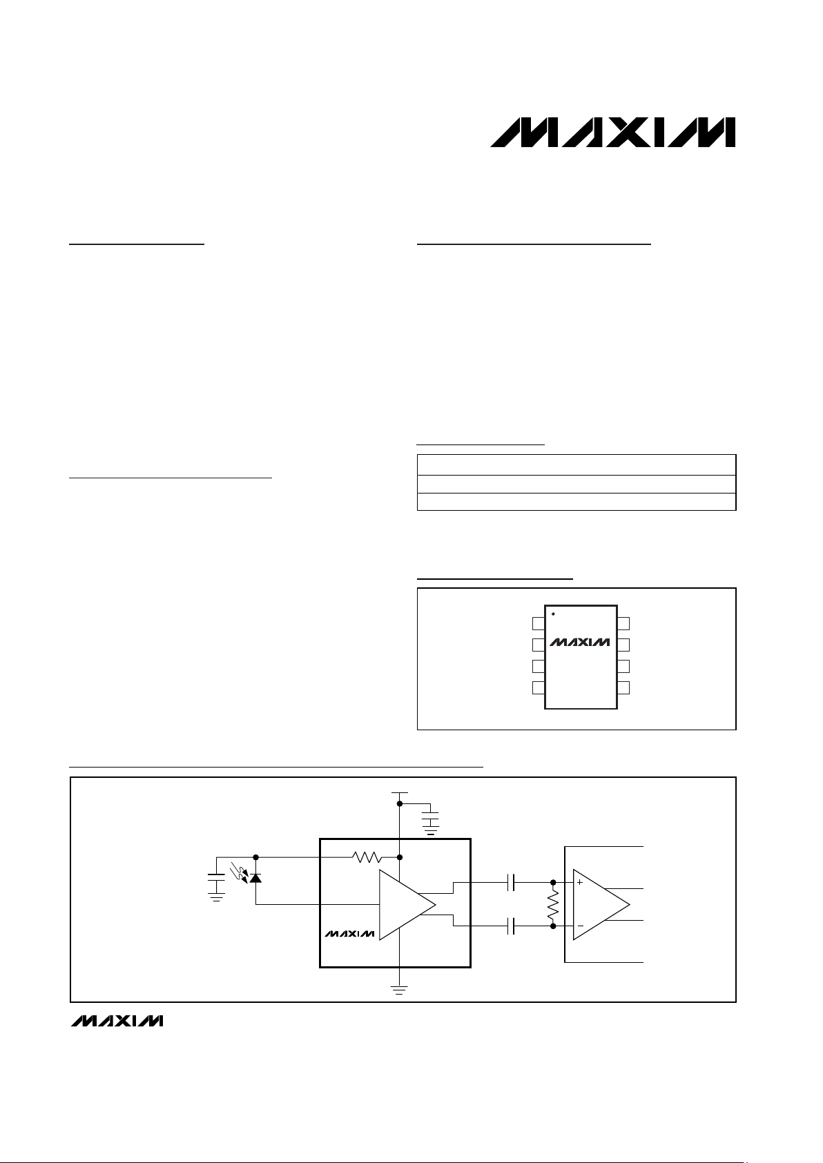
Typical Application Circuit
Pin Configuration
Ordering Information
PART TEMP. RANGE PIN-PACKAGE
MAX3864ESA
-40°C to +85°C
8 SO
MAX3864E/D
-40°C to +85°C
Dice*
* Dice are designed to operate with junction temperatures of -40°C
to +140°C but are tested and guaranteed only at T
A
= +25°C.
Page 2
MAX3864
2.5Gbps, +3V to +5.5V, Wide Dynamic Range
Transimpedance Preamplifier
2 _______________________________________________________________________________________
ABSOLUTE MAXIMUM RATINGS
Stresses beyond those listed under “Absolute Maximum Ratings” may cause permanent damage to the device. These are stress ratings only, and functional
operation of the device at these or any other conditions beyond those indicated in the operational sections of the specifications is not implied. Exposure to
absolute maximum rating conditions for extended periods may affect device reliability.
Note 1: Source capacitance represents the total capacitance at the IN pin during characterization of noise and bandwidth parame-
ters. Noise and bandwidth will be affected by the source capacitance. See the Typical Operating Characteristics for more
information.
Note 2: Input-referred noise is calculated as (RMS output noise) / (Gain at f = 10MHz). Noise density is (Input-Referred Noise) /
(Bandwidth)
1/2
. No external filters are used for the noise measurements.
Note 3: Deterministic jitter is defined as the arithmetic sum of pulse-width distortion and pattern dependent jitter measured with a
repeating 20-bit pattern of 00111110101100000101 (K28.5). See Typical Operating Characteristics.
Supply Voltage (V
CC
- GND).................................-0.5V to +6.0V
IN Current..............................................................-4mA to +4mA
FILTER Current......................................................-8mA to +8mA
Voltages at OUT+, OUT- .................(V
CC
- 1.5V) to (VCC+ 0.5V)
Continuous Power Dissipation (T
A
= +85°C)
8-Pin SO package (derate 6.7mW/°C above +85°C) ..436mW
Storage Temperature Range .............................-55°C to +150°C
Operating Junction Temperature ......................-55°C to +150°C
Processing Temperature (die) .........................................+400°C
Lead Temperature (soldering, 10s) .................................+300°C
ELECTRICAL CHARACTERISTICS
(VCC= +3.0V to +5.5V, 100Ω load between OUT+ and OUT-, 0.1µF coupling capacitors on OUT+ and OUT-, TA= -40°C to +85°C,
unless otherwise noted. Typical values are at +3.3V, source capacitance = 0.85pF, and T
A
= +25°C.) (Note 1)
PARAMETER CONDITIONS MIN TYP MAX UNITS
Input Bias Voltage 0.66 0.83 0.99 V
Supply Current 34 63 mA
Transimpedance Differential, measured with 40µAp-p input 2100 2750 3400 Ω
Output Impedance Single ended (per side) 48 50 52 Ω
Maximum Differential Output Voltage
Input = 2mAp-p with 100Ω differential output
termination
220 380 575 mVp-p
Filter Resistor 600 750 930 Ω
AC Input Overload 2 mAp-p
DC Input Overload 1mA
Input-Referred RMS Noise 490 668 nA
Input-Referred Noise Density Bandwidth = 2.0GHz (Note 2) 11 pA/√(Hz)
Small-Signal Bandwidth 1525 2000 MHz
Low-Frequency Cutoff -3dB, input ≤ 20µADC 30 kHz
Transimpedance Linear Range
Gain at 40µAp-p is within 5% of the smallsignal gain
40 µAp-p
3.13V < VCC < 5.5V (Note 3) 24 67
Deterministic Jitter
3.0V ≤ V
CC
≤ 3.13V (Note 3) 24 77
ps
Power-Supply Rejection Ratio (PSRR)
Output referred, f < 2MHz,
PSRR = -20log(∆V
OUT
/∆Vcc)
50 dB
Page 3
MAX3864
2.5Gbps, +3V to +5.5V, Wide Dynamic Range
Transimpedance Preamplifier
_______________________________________________________________________________________ 3
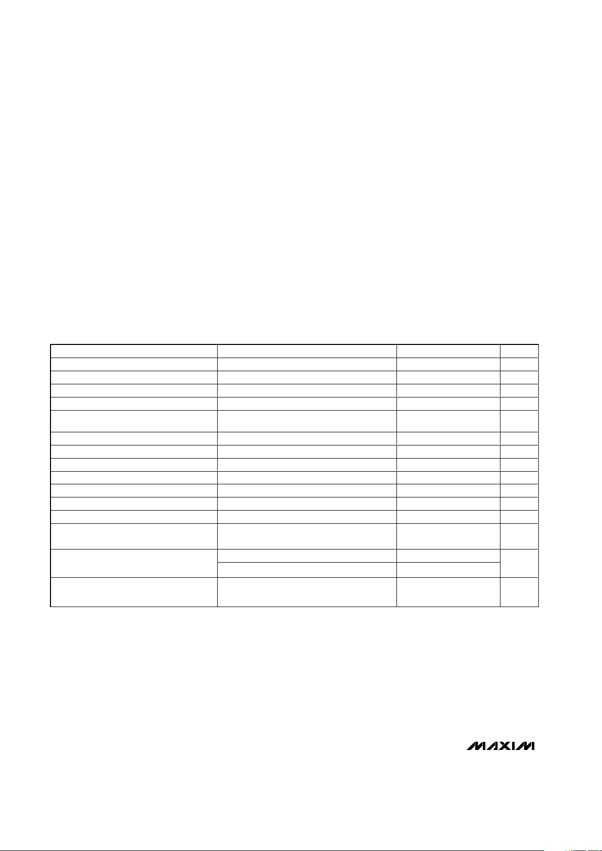
200
300
250
400
350
550
500
450
600
-40 0-20 20406080100
INPUT-REFERRED RMS NOISE
vs. TEMPERATURE
MAX3864 toc01
JUNCTION TEMPERATURE (°C)
INPUT-REFERRED NOISE (nA
RMS
)
CIN = 1.5pF
CIN = 1.0pF
CIN = 0.5pF
CIN IS SOURCE CAPACITANCE
PRESENTED TO DIE, INCLUDES
PACKAGE PARASITIC, PIN DIODE,
AND PARASITIC INTERCONNECT
CAPACITANCE.
50
55
65
60
70
75
FREQUENCY RESPONSE
MAX3864 toc02
FREQUENCY (MHz)
TRANSIMPEDANCE (dBΩ)
110010 1k 10k
0
30
20
10
40
50
60
70
80
90
100
10 100 1000 10,000
DETERMINISTIC JITTER
vs. INPUT AMPLITUDE
MAX3864 toc03
INPUT CURRENT AMPLITUDE (µAp-p)
PEAK-TO-PEAK JITTER (ps)
0
300
200
100
400
500
600
700
800
900
1000
1 10 100 1000
INPUT-REFERRED RMS NOISE CURRENT
vs. DC INPUT CURRENT
MAX3864 toc04
DC INPUT CURRENT (µA)
INPUT-REFERRED NOISE (nA
RMS
)
60
63
62
61
65
64
69
68
67
66
70
-40-200 20406080100
SMALL-SIGNAL TRANSIMPEDANCE
vs. TEMPERATURE
MAX3864 toc05
AMBIENT TEMPERATURE (°C)
TRANSIMPEDANCE dBΩ)
1.4
1.6
1.5
1.9
1.8
1.7
2.2
2.1
2.0
2.3
-40 0 20-20 40 60 80 100
BANDWIDTH vs. TEMPERATURE
MAX3864 toc06
JUNCTION TEMPERATURE (°C)
BANDWIDTH (GHz)
CIN = 1.5pF
CIN = 1.0pF
CIN = 0.5pF
CIN IS SOURCE CAPACITANCE
PRESENTED TO DIE, INCLUDES
PACKAGE PARASITIC, PIN DIODE,
AND PARASITIC INTERCONNECT
CAPACITANCE.
300
360
340
320
400
380
480
460
440
420
500
-40-200 20406080100
DIFFERENTIAL OUTPUT AMPLITUDE
vs. TEMPERATURE
MAX3864 toc07
AMBIENT TEMPERATURE (°C)
DIFFERENTIAL OUTPUT AMPLITUDE (mVp-p)
INPUT = 2mA
EYE DIAGRAM (INPUT = 2mAp-p)
MAX3864 toc11
80ps/div
50mV/div
INPUT = 2
13
-1 PRBS WITH 72 CID
V
CC
= 3.0V AT TA = -40°C
EYE DIAGRAM (INPUT = 2mAp-p)
MAX3864 toc12
80ps/div
50mV/div
INPUT = 2
13
-1 PRBS WITH 72 CID
V
CC
= 3.13V AT TA = -40°C
Typical Operating Characteristics
(V
CC
= 3.3V, TA = +25°C and MAX3864 EV kit source capacitance = 0.85pF, unless otherwise noted).
Page 4
MAX3864
Detailed Description
The MAX3864 transimpedance amplifier is designed for
2.5Gbps fiber optic applications. As shown in Figure 1,
the MAX3864 comprises a transimpedance amplifier, a
voltage amplifier, an output buffer, an output filter, and
a DC cancellation circuit.
Transimpedance Amplifier
The signal current at the input flows into the summing
node of a high-gain amplifier. Shunt feedback through
RFconverts this current to a voltage. Schottky diodes
clamp the output voltage for large input currents
(Figure 2).
Voltage Amplifier
The voltage amplifier converts single-ended signals to
differential signals and introduces a voltage gain.
Output Buffer
The output buffer provides a back-terminated voltage
output. The buffer is designed to drive a 100Ω differential load between OUT+ and OUT-. The output voltage
is divided between internal 50Ω load resistors and the
external load resistor. In the typical operating circuit,
this creates a voltage-divider with a ratio of 1/2. The
MAX3864 can also be terminated with higher output
impedances, which increases gain and output voltage
swings.
2.5Gbps, +3V to +5.5V, Wide Dynamic Range
Transimpedance Preamplifier
4 _______________________________________________________________________________________
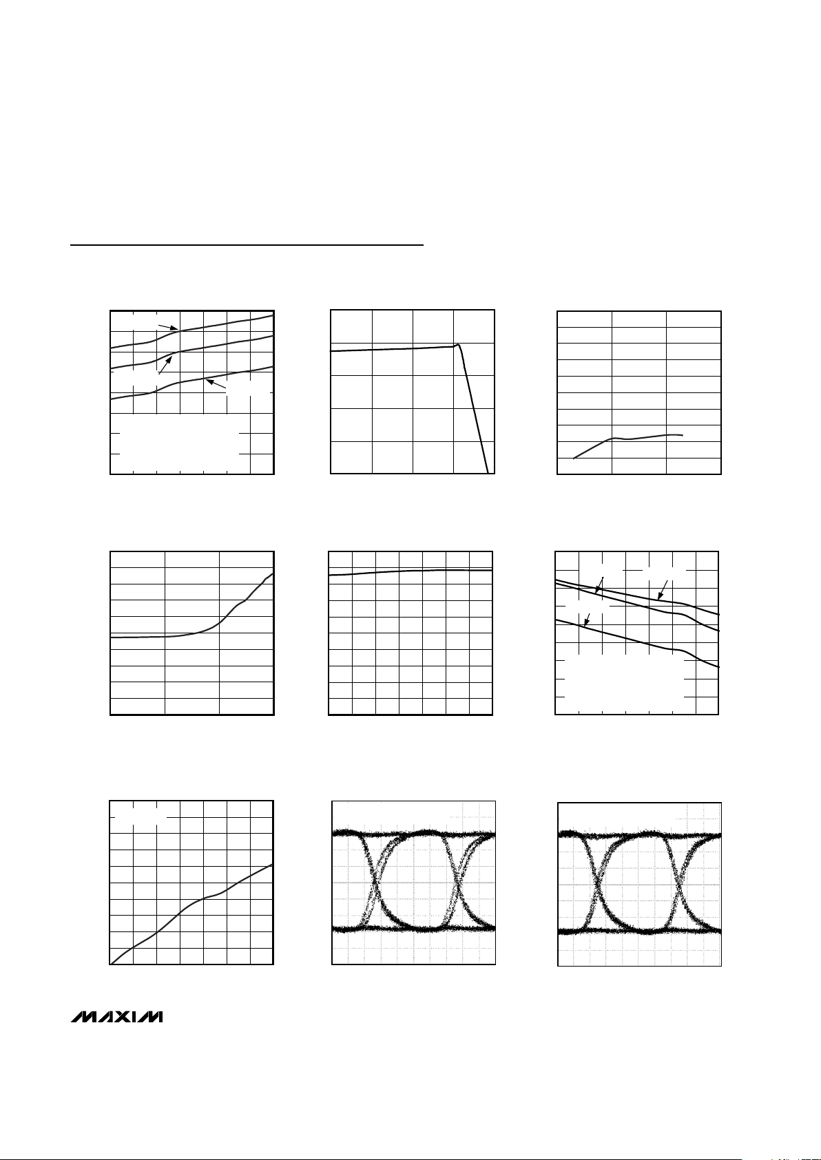
Typical Operating Characteristics (continued)
V
CC
= 3.3V, TA = +25°C and MAX3864 EV kit source capacitance = 0.85pF, unless otherwise noted).
Pin Description
200
100
0
-100
-200
-100 0-50 50 100
DC TRANSFER FUNCTION
MAX3864 toc10
INPUT CURRENT (µA)
DIFFERENTIAL OUITPUT VOLTAGE (mVp-p)
EYE DIAGRAM (INPUT = 20µAp-p)
MAX3864 toc09
80ps/div
10mV/div
INPUT = 223 -1 PRBS
PIN NAME FUNCTION
1VCCSupply Voltage
2 N.C. No Connection
3 IN Amplifier Input
4 FILTER
Provides bias voltage for the photodiode through a 750Ω resistor to V
CC
. When grounded, this pin
disables the DC cancellation amplifier to allow a DC path from IN to OUT+ and OUT- for testing.
5 GND Ground
6 OUT- Inverting Output. Current flowing into IN causes V
OUT-
to decrease.
7 OUT+ Noninverting Output. Current flowing into IN causes V
OUT+
to increase.
8 GND Ground
EYE DIAGRAM (INPUT = 2mAp-p)
MAX3864 toc08
80ps/div
50mV/div
INPUT = 223 -1 PRBS
Page 5

For optimum supply-noise rejection, the MAX3864
should be terminated with a differential load. If a singleended output is required, the unused output should be
terminated with 50Ω to VCC. The MAX3864 will not drive
a DC-coupled, 50Ω grounded load.
Output Filter
The MAX3864 includes a one-pole lowpass filter that
limits the circuit bandwidth and improves noise performance.
DC Cancellation Circuit
The DC cancellation circuit uses low-frequency feedback to remove the DC component of the input signal
(Figure 3). This feature centers the input signal within the
transimpedance amplifier’s linear range, thereby reducing pulse-width distortion (PWD) on large input signals.
The DC cancellation circuit is internally compensated
and therefore does not require external capacitors. This
circuit minimizes PWD for data sequences that exhibit a
50% duty cycle and mark density. A duty cycle or mark
density significantly different from 50% causes the
MAX3864 to generate PWD.
DC cancellation current is drawn from the input and
creates noise. For low-level signals with little or no DC
component, this is not a problem. Amplifier noise will
increase for signals with significant DC component (see
Typical Operating Characteristics).
MAX3864
2.5Gbps, +3V to +5.5V, Wide Dynamic Range
Transimpedance Preamplifier
_______________________________________________________________________________________ 5
VOLTAGE
AMPLIFIER
TRANSIMPEDANCE
AMPLIFIER
OUTPUT
BUFFER
OUTPUT
FILTER
OUT+
50Ω
50Ω
OUT-
V
CC
RF = 1k
V
CC
LOWPASS FILTER
750Ω
FILTER
IN
GND
DC CANCELLATION
CIRCUIT
DISABLE
MAX3864
Figure 1. Functional Diagram
AMPLITUDE
OUTPUT (LARGE SIGNALS)
TIME
OUTPUT (SMALL SIGNALS)
Figure 2. Limited Output
AMPLITUDE INPUT FROM PHOTODIODE
TIME
INPUT (AFTER DC CANCELLATION)
Figure 3. DC Cancellation Effect on Input
Page 6

Applications Information
Optical Power Relations
Many of the MAX3864 specifications relate to the input
signal amplitude. When working with fiber optic receivers,
the input is usually expressed in terms of average optical
power and extinction ratio. Figure 4 shows relations that
are helpful for converting optical power to input signal
when designing with the MAX3864.
Optical power relations are shown in Table 1; the definitions are true if the average duty cycle and mark density of the input data are 50%.
Optical Sensitivity Calculations
The MAX3864 input-referred RMS noise current (IN)
generally determines the receiver sensitivity. To obtain
a system bit-error rate (BER) of 1E-10, the minimum signal-to-noise ratio (SNR) is 12.7. The input sensitivity,
expressed in average power, can be estimated as:
where ρ is the photodiode responsivity, including fiberto-photodiode coupling efficiency in A/W and I
N
in µA.
For example, if SNR = 12.7, I
N
= 0.490µA, re= 10, and
ρ = 1, then sensitivity is -24dBm.
Input Optical Overload
The overload is the largest input that the MAX3864
accepts while meeting deterministic jitter specifications.
The optical overload can be estimated in terms of average power with the following equation (assumes
r
e
= ∞):
Optical Linear Range
The MAX3864 has high gain, which limits the outputs
when the input signal exceeds 40µAp-p. The MAX3864
operates in a linear range for inputs not exceeding:
Layout Considerations
Use good high-frequency design and layout techniques.
The use of a multilayer circuit board with separate ground
and power planes is recommended. Connect the GND
pins to the ground plane with the shortest possible traces.
Noise performance and bandwidth will be adversely
affected by capacitance at the IN pin. Minimize capacitance on this pin, and select a low-capacitance photodiode. Assembling the MAX3864 in die form using chip and
wire technology provides the best possible performance.
Figure 5 shows the recommended layout for a TO
header.
The SO package version of the MAX3864 is offered as an
easy way to characterize the circuit and to become familiar with the circuit’s operation, but it does not offer optimum performance. When using the SO version of the
MAX3864, the package capacitance adds approximately
0.3pF at the input. The PC board between the MAX3864
input and the photodiode also adds parasitic capacitance. Keep the input line short, and remove power and
ground planes beneath it.
GND
Connect GND as close to the AC ground of the photodetector diode as possible. The photodetector AC ground is
usually the ground of the filter capacitor from the photodetector cathode. The total loop (from GND, through the
bypass capacitor and the diode, and back to IN) should
be no more than approximately 1/5th of a wavelength.
Overload 10log
2mAp - p 1000
2
dBm=
×
ρ
Sensitivity=10log
SNR
2
dBm
×+
()
−
()
×
Ir
r
Ne
e
1
1 1000ρ
MAX3864
2.5Gbps, +3V to +5.5V, Wide Dynamic Range
Transimpedance Preamplifier
6 _______________________________________________________________________________________
PO
PI
P
AVG
TIME
POWER
P
IN
Figure 4. Optical Power Relations
PARAMETER SYMBOL RELATION
Average Power P
AVE
P
AVE
= (P0 + P1) / 2
Extinction Ratio r
e
re = P1 / P
0
Optical Power of a 1 P
1
P1 = 2P
AVEre
/ (re + 1)
Optical Power of a 0 P
0
P0 = 2P
AVE
/ (re + 1)
Signal Amplitude P
IN
PIN = P1 - P0 = 2P
AVE
(re - 1) / (re + 1)
Table 1. Optical Power Relations
Note: Assuming a 50% average input duty cycle and mark
density.
Linear Range = 10log
4-
2
dBm
0 1 1000
1
µ+
()
×
−
()
Ap p r
r
e
e
ρ
Page 7

MAX3864
2.5Gbps, +3V to +5.5V, Wide Dynamic Range
Transimpedance Preamplifier
_______________________________________________________________________________________ 7
IN
V
CC
V
CC
GND
200Ω
Figure 6. Equivalent Input Circuit
CASE IS GROUND
TOP VIEW OF TO-46 HEADER
C
FILTER
V
CC
PHOTODIODE
MAX3864
OUT+
OUT-
Figure 5. Suggested Layout for TO-46 Header
Photodiode Filter
Supply voltage noise at the photodiode cathode produces a current I = CPD∆V / ∆t, which reduces the
receiver sensitivity (CPDis the photodiode capacitance). The filter resistor of the MAX3864, combined
with an external capacitor, can be used to reduce this
noise (see the Typical Application Circuit). Current generated by supply noise voltage is divided between
C
FILTER
and CPD. The input noise current due to supply noise is (assuming the filter capacitor is much larger than the photodiode capacitance):
If the amount of tolerable noise is known, the filter
capacitor can be easily selected:
For example, with a maximum noise voltage equal to
100mVp-p, CPD= 0.85pF, R
FILTER
= 750Ω, and I
NOISE
selected to be 250nA (half of the MAX3864’s input noise):
Wire Bonding
For high current density and reliable operation, the
MAX3864 uses gold metalization. Connections to the
die should be made with gold wire only, using ballbonding. Wedge bonding is not recommended. Die
thickness is typically 15mils (0.375mm).
C=
100mV
FILTER
()()
()( )
=
085
750 250
453
.pF
nA
pF
Ω
C=
V
FILTER
NOISE
()()
()()
C
RI
PD
FILTER NOISE
I=
V
NOISE
NOISE
()()
()()
C
RC
PD
FILTER FILTER
Page 8

MAX3864
2.5Gbps, +3V to +5.5V, Wide Dynamic Range
Transimpedance Preamplifier
8 _______________________________________________________________________________________
V
CC
OUT+
OUT-
GND
50Ω 50Ω
Figure 7. Equivalent Output Circuit
Page 9

MAX3864
2.5Gbps, +3V to +5.5V, Wide Dynamic Range
Transimpedance Preamplifier
_______________________________________________________________________________________ 9
30mils
50mils
1.27mm
OUT+
GND
OUT-
GND
V
CC
INPUT FILTER
(0.762mm)
Chip Information
TRANSISTOR COUNT: 320
PROCESS: BIPOLAR (SILICON GERMANIUM)
Chip Topography
Page 10

Package Information
MAX3864
2.5Gbps, +3V to +5.5V, Wide Dynamic Range
Transimpedance Preamplifier
10 ______________________________________________________________________________________
SOICN.EPS
Page 11

MAX3864
2.5Gbps, +3V to +5.5V, Wide Dynamic Range
Transimpedance Preamplifier
______________________________________________________________________________________ 11
NOTES
Page 12

MAX3864
2.5Gbps, +3V to +5.5V, Wide Dynamic Range
Transimpedance Preamplifier
Maxim cannot assume responsibility for use of any circuitry other than circuitry entirely embodied in a Maxim product. No circuit patent licenses are
implied. Maxim reserves the right to change the circuitry and specifications without notice at any time.
12 ____________________Maxim Integrated Products, 120 San Gabriel Drive, Sunnyvale, CA 94086 408-737-7600
© 2000 Maxim Integrated Products Printed USA is a registered trademark of Maxim Integrated Products.
NOTES
 Loading...