

Page 1
General Description
The MAX3770 is a 2.125Gbps Fibre Channel repeater
IC. The MAX3771 provides a pin-compatible solution
for 1.063Gbps Fibre Channel. Both devices are optimized for use in Fibre Channel arbitrated-loop applications and operate from a 3.3V supply.
The MAX3770 is compatible with Fibre Channel jitter tolerance requirements and can recover data signals with up
to 0.7 unit interval (UI) jitter. The circuit’s fully integrated
phase-locked loop (PLL) provides a frequency lock indication and does not need an external reference clock.
The MAX3770 provides low-jitter CML clock and data
outputs. To reduce the external parts count, all signal
inputs and outputs are internally terminated. The
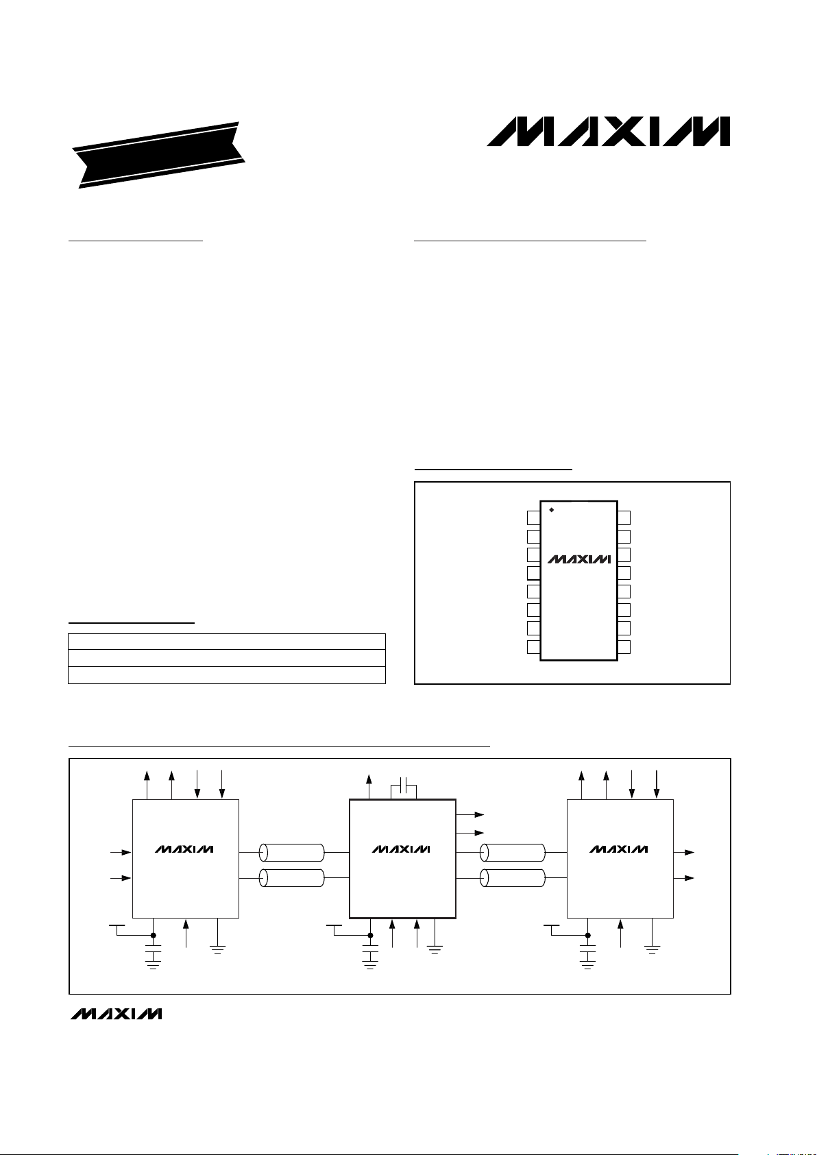
MAX3770/MAX3771 are available in 16-pin QSOP
packages.
________________________Applications
2.125Gbps Fibre Channel Storage Area Networks
1.063Gbps Fibre Channel Fibre Channel Hubs
Fibre Channel Storage Systems
Features
♦ Meet Fibre Channel Jitter Tolerance Requirements
♦ 3.0V to 3.6V Operation
♦ Internally Terminated Data and Clock I/O
♦ Reference Clock Not Required
♦ Frequency Lock Indication
♦ Low Power Consumption
215mW at 3.3V (MAX3770)
190mW at 3.3V (MAX3771)
MAX3770/MAX3771
2.125Gbps/1.063Gbps, 3.3V
Fibre Channel Repeaters
________________________________________________________________ Maxim Integrated Products 1
16
15
14
13
12
11
10
9
1
2
3
4
5
6
7
8
FILT+ LOCK
CLK+
CLK-
CLKEN
GND
OUT+
OUT-
LOCKEN
TOP VIEW
MAX3770
MAX3771
QSOP
FILT-
GND
GND
IN+
IN-
V
CC
V
CC
Pin Configuration
3.3V
Z
o
= 75Ω
PORT BYPASS CIRCUIT
DATA REPEATER
Zo = 75Ω
MAX3770
MAX3771
CLK+
CLK-
GND
LOCKEN
CLKEN
V
CC
0.22µF
0.1µF
OUT+
OUT-
IN+
IN-
FILT-
FILT+
LOCK
3.3V
MAX3750
MAX3751
GND
SEL
V
CC
0.1µF
OUT+
OUT-
IN+
IN-
LIN+
LIN-
LOUT-
LOUT+
PORT BYPASS CIRCUIT
3.3V
MAX3750
MAX3751
GND
SEL
V
CC
0.1µF
OUT+
OUT-
IN+
IN-
LIN+
LIN-
LOUT-
LOUT+
Zo = 75Ω
Zo = 75Ω
Typical Application Circuit
19-1634; Rev 0; 1/00
EVALUATION KIT
AVAILABLE
Ordering Information
*Future product—contact factory for availability.
MAX3771CEE*
0°C to +70°C 16 QSOP
PART
MAX3770CEE
0°C to +70°C
TEMP. RANGE PIN-PACKAGE
16 QSOP
For free samples and the latest literature, visit www.maxim-ic.com or phone 1-800-998-8800.
For small orders, phone 1-800-835-8769.
Page 2
MAX3770/MAX3771
2.125Gbps/1.063Gbps, 3.3V
Fibre Channel Repeaters
2 _______________________________________________________________________________________
ABSOLUTE MAXIMUM RATINGS
DC ELECTRICAL CHARACTERISTICS
(VCC= +3.0V to +3.6V, TA= 0°C to +70°C, unless otherwise noted. Typical values are at TA= +25°C.)
Stresses beyond those listed under “Absolute Maximum Ratings” may cause permanent damage to the device. These are stress ratings only, and functional
operation of the device at these or any other conditions beyond those indicated in the operational sections of the specifications is not implied. Exposure to
absolute maximum rating conditions for extended periods may affect device reliability.
Note 1: Supply current includes output currents.
Supply Voltage, V
CC
..............................................-0.5V to +5.0V
Pin Voltage Levels (IN+, IN-, FILT+, FILT-,
LOCKEN, CLKEN, LOCK) ....................-0.5V to (V
CC
+ 0.5V)
LOCK Output Current .........................................-1mA to +10mA
CML Output Currents OUT+, OUT-,
CLK+, CLK-.................................................-22mA to +22mA
Continuous Power Dissipation (T
A
= +70°C)
16-Pin TQFP (derate 6.7mW/°C above +70°C)..........533mW
Operating Temperature Range...............................0°C to +70°C
Storage Temperature Range .............................-55°C to +150°C
Processing Temperature (die) .........................................+400°C
Lead Temperature (soldering, 10s) .................................+300°C
CLKEN = GND
CLKEN = V
CC
OUT+, OUT-, CLK+, CLK-
IOH= -100µA
IOL= +1mA
R
LOAD
= 150Ω, Figure 1
Sum of I
OUT+
and I
OUT-
CONDITIONS
Ω132 150 181Differential Output Resistance
Ω132 150 181Differential Input Resistance
µA-5 +5
CLOCKEN and LOCKEN
Input Current
VVCC- 1.03Voltage at FILT+, FILT-
VVCC- 0.45Input Common-Mode Voltage
mVp-p200 2200Differential Input Voltage Swing
57
81 112
63
V2.4LOCK Output High
V0.7LOCK Output Low
mA
67.5 91
mVp-p400 780 1000
Differential Voltage Signal at
OUT or CLOCK
mA10.5
Output Current at OUT or
CLOCK
UNITSMIN TYP MAXPARAMETER
Supply Current (Note 1)
MAX3771
MAX3770
MAX3771
MAX3770
Page 3
ps/rms
MAX3770/MAX3771
2.125Gbps/1.063Gbps, 3.3V
Fibre Channel Repeaters
_______________________________________________________________________________________ 3
AC ELECTRICAL CHARACTERISTICS
(VCC= +3.0V to +3.6V, TA= 0°C to +70°C, unless otherwise noted. Typical values are at TA= +25°C.)
Note 2: K28.7+ pattern: 0011111000
Note 3: Compliant random pattern (CRPAT) in hex:
Pattern No. of Occurrences
3EAA2AAAAA 6
3EAAA6A5A9 1
86BA6C6475 D0E8DCA8B4 7949EAA665 16
72319A95AB 1
C16AAA9AA6 1
Note 4: K28.5± pattern: 00111110101100000101
Note 5: Random and deterministic jitter generation at 2.125Gbps is measured with 0.38UI deterministic jitter, and 0.22UI random
jitter (BER = 1 x 10
-12
) applied to the input. Random and deterministic jitter generation at 1.063Gbps is measured with
0.18UI deterministic jitter, and 0.08UI random jitter (BER = 1 x 10
-12
) applied to the input.
Jitter tolerance at 2.125Gbps is measured with 0.38UI deterministic jitter and 0.22UI random jitter (BER = 1 x 10
-12
) applied
to the input. Jitter tolerance at 1.063Gbps is measured with 0.18UI deterministic jitter, and 0.08UI jitter (BER = 1 x 10
-12
)
applied to the input.
Note 6: Compliant jitter tolerance pattern in hex (CJTPAT):
Pattern No. of Occurrences
3EAA2AAAAA 6
3EAAA6A5A9 1
871E3871E3 41
871E3870BC78F4AAAAAA 1
AAAAAAAAAA 12
AAA15555E3 871E3871E1 1
AB9C9686E6 1
C16AAA9AA6 1
Note 7: Jitter tolerance measurements at 85kHz and 1270kHz are limited by test equipment. Actual jitter tolerance > indicated.
TA= +25°C
CONDITIONS
Input = CRPAT (Note 3)
Input = CRPAT (Notes 3, 5)
Input = K28.5± (Note 4)
Input = CRPAT (Notes 3, 5)
ps
p-p
15.6 22
3.9 7.3
2.3 3.1
27 48
UIJitter Tolerance
UNITSMIN TYP MAXPARAMETER
Deterministic Jitter Generation
f = 85kHz (Note 7) 1.5 4.22
ps135 170Edge Speed
TA= +25°C ps
RMS
3.4 5.3
Random Jitter Generation at
Data Output
Input = K28.7+ (Note 2)
20% to 80%
f = 1270kHz (Note 7) 0.1 0.89
Input = CJTPAT (Note 6) ms4.4CDR Lock Time from Start
f = 10MHz 0.36
TA= +25°C (Note 5),
input = CJTPAT (Note 6)
ps50 240 300Clock to Q Delay
ps1000 1500Propagation Delay
Input = K28.7+ (Note 2)
TA= +25°C ps
RMS
3.9
Random Jitter Generation at
Data Output
Input = CRPAT (Note 3) 2.3
Input = CRPAT (Notes 3, 5) 3.4
Input = K28.5± (Note 4)
TA= +25°C
ps
p-p
17
Deterministic Jitter Generation
Input = CRPAT (Notes 3, 5) ps
p-p
36
f = 42.5kHz
TA= +25°C (Note 5),
input = CJTPAT (Note 6),
BER = IE-12
UI
3.1
Jitter Tolerance
f = 635kHz 0.54
f = 5MHz 0.3
OPERATION AT 2.125Gbps
OPERATION AT 1.063Gbps
Page 4

MAX3770/MAX3771
2.125Gbps/1.063Gbps, 3.3V
Fibre Channel Repeaters
4 _______________________________________________________________________________________
MAX3770
JITTER TRANSFER
MAX3770/1 toc01
JITTER FREQUENCY (Hz)
JITTER TRANSFER (dB)
5
-20
-25
-15
-10
-5
0
1k 1M 10M 100M10k 100k 1G
CJTPAT
V
CC
= 3.3V
C
F
= 0.1µF
MAX3770
JITTER TOLE RANCE
MAX3770/1 toc02
JITTER FREQUENCY (Hz)
SINUSOIDAL INPUT JITTER (UI)
0.01
0.1
1
10
1M 10M 100M10k 100k
CJTPAT
V
CC
= 3.3V
C
F
= 0.1µF
ADDITIONAL 0.6UI DJ AND RJ
APPLIED ABOVE 10MHz
FIBRE CHANNEL
SINUSOIDAL
JITTER MASK
DATA
VCC = 3.3V
CJTPAT
VCLK-
CLOCK
MAX3770
RECOVERED DATA AND CLOCK SIGNALS
MAX3770/1 toc03
100ps/div
Typical Operating Characteristics
(VCC= +3.3V, TA = +25°C, unless otherwise noted.)
Pin Description
NAMEPIN FUNCTION
1 FILT+ PLL Loop Filter Connection. Connect a 0.22µF capacitor between FILT+ and FILT-.
2 FILT- PLL Loop Filter Connection. Connect a 0.22µF capacitor between FILT+ and FILT-.
3, 6, 12 GND Ground
4 IN+ Positive CML Data Input (Figure 3)
5 IN- Negative CML Data Input (Figure 3)
7, 8 V
CC
Supply Voltage
9 LOCKEN When this input is forced high, the lock indicator is enabled. Ground for normal operation.
10 OUT- Negative 75Ω CML Data Output (Figure 4)
11 OUT+ Positive 75Ω CML Data Output (Figure 4)
13 CLKEN When this input is forced high, the clock output is enabled. Ground for normal operation.
14 CLK-
Negative 75Ω CML Clock Output (Figure 4). Enabled when CLKEN is forced high; disabled when CLKEN
is forced low.
15 CLK+
Positive 75Ω CML Clock Output (Figure 4). Enabled when CLKEN is forced high; disabled when CLKEN is
forced low.
16 LOCK
Frequency Lock Indicator. High level indicates the PLL is frequency-locked. Disabled when LOCKEN is
forced low. The output of the LOCK pin may chatter when large jitter is applied to the input.
Page 5

MAX3770/MAX3771
2.125Gbps/1.063Gbps, 3.3V
Fibre Channel Repeaters
_______________________________________________________________________________________ 5
PHASE/FREQ
DETECTOR
CLK+
CLK-
OUT +
OUT -
IN+
IN-
LOCK
LOOP
FILTER
CLKEN
LOCKEN
LOCK
TTL
FILT+
0.22µF
FILT-
150Ω
75Ω
75Ω
75Ω
75Ω
V
CC
V
CC
LATCH
D
Q
VCO
MAX3770
MAX3771
Figure 2. Functional Diagram
200mVp-p MIN
500mVp-p MAX
400mVp-p MIN
1000mVp-p MAX
V
OUT
+
V
OUT
-
(V
OUT
+) - (V
OUT
-)
Figure 1. Example of Output Signal with R
LOAD
= 150Ω
Page 6

MAX3770/MAX3771
2.125Gbps/1.063Gbps, 3.3V
Fibre Channel Repeaters
6 _______________________________________________________________________________________
Detailed Description
Figure 2 shows the functional diagram of the MAX3770
Fibre Channel repeater IC. The MAX3770 consists of a
fully integrated phased-lock loop (PLL), CML input and
output buffers, and a data latch. The PLL consists of a
phase/frequency detector (PFD), a loop filter, and a
voltage-controlled oscillator (VCO). The input and output signal buffers employ low-noise CML architecture
and are terminated on-chip.
Phase and Frequency Detector
The phase/frequency detector generates an output signal
that reflects the phase relationship between the incoming
data and the internal clock generated by the VCO. Data
recovery is accomplished by feedback in the PLL, which
drives the error voltage to zero, aligning the falling edge
of the recovered clock to the center of the data eye.
The phase frequency detector generates a frequency
lock indication that can be monitored at the LOCK pin
(Table 1). When the PLL is frequency-locked onto the
incoming data, lock transitions high.
VCO and Latch
The fully integrated VCO contains an internal current reference and filter circuitry to minimize the influence
of VCCnoise. The VCO is trimmed to 2.125GHz
(MAX3770) and creates a clock output with frequency
proportional to the control voltage applied by the loop
filter. Data recovery is accomplished by using the recovered clock signal to latch the incoming data to the CML
output buffers, significantly reducing the output jitter.
Applications Information
Figures 3 and 4 show models for the MAX3770/MAX3771
inputs and outputs, including package parasitics. Figure
5 shows typical 50Ω termination applications.
Design Procedure
The MAX3770’s performance can be greatly affected
by circuit board layout and design. Use good high-frequency design techniques, including minimizing
ground inductance and using fixed-impedance transmission lines on the data and clock signals. All IN,
OUT, and CLK pins can be connected with 0.1µF or
0.01µF coupling capacitors. If DC coupling is desired,
pay particular attention to the DC voltage and current
requirements at the pins of interest (see DC Electrical
Characteristics). The MAX3750/MAX3751 port bypass
circuit can be DC-coupled to the MAX3770/MAX3771
repeater. A 0.22µF capacitor should be used for the
loop filter.
Control Functions
The lock enable (LOCKEN) and clock enable (CLKEN)
pins can be configured to control the PLL’s clock.
Table 1 shows the operational modes available.
Figure 3. Input Structure
Figure 4. Output Structure
ESD
STRUCTURES
IN+
PACKAGE
1.5nH
1.5nH
0.2pF
0.4pF
0.4pF
V
CC
- 0.450V
0.2pF
75Ω
75Ω
1kΩ
V
CC
ESD
STRUCTURES
10.5mA
OUT-
OUT+
V
CC
PACKAGE
1.5nH
1.5nH
0.2pF
0.4pF
0.4pF
0.2pF
75Ω
75Ω
Page 7

MAX3770/MAX3771
2.125Gbps/1.063Gbps, 3.3V
Fibre Channel Repeaters
_______________________________________________________________________________________ 7
Figure 5. 50Ω Termination Applications
MAX3770
MAX3771
300Ω
300Ω
Z
o
= 50Ω
100Ω DIFF
(LOOKING IN)
150Ω DIFF
(LOOKING OUT)
100Ω DIFF
(LOOKING IN)
75Ω DIFF
(LOOKING OUT)
Zo = 50Ω
Z
o
= 50Ω
Z
o
= 50Ω
0.1µF
0.1µF
0.1µF
0.1µF
IN+
IN-
OUT+
OUT-
MAX3770
MAX3771
176Ω
43Ω
43Ω
43Ω
43Ω
176Ω
Z
o
= 50Ω
Zo = 50Ω
Z
o
= 50Ω
Z
o
= 50Ω
IN+
IN-
OUT+
OUT-
Table 1. Output States When Using
Control Functions
Chip Topography
FILT+
FILT-
GND
IN+
IN-
GND
V
CC
V
CC
LOCK
CLK+
CLK-
CLKEN
GND
OUT+
LOCKEN
OUT-
0.067"
(1.702mm)
0.066"
(1.676mm)
TRANSISTOR COUNT: 1217
SUBSTRATE CONNECTED to GND
Enabled
Disabled
Enabled
CLOCK
V
CC
V
CC
Enabled
V
CC
GND Enabled
GND V
CC
Disabled
LOCKEN CLKEN LOCK
INPUT PIN LEVEL OUTPUT FUNCTION
DisabledGND GND Disabled
Page 8

MAX3770/MAX3771
2.125Gbps/1.063Gbps, 3.3V
Fibre Channel Repeaters
Maxim cannot assume responsibility for use of any circuitry other than circuitry entirely embodied in a Maxim product. No circuit patent licenses are
implied. Maxim reserves the right to change the circuitry and specifications without notice at any time.
8 _____________________Maxim Integrated Products, 120 San Gabriel Drive, Sunnyvale, CA 94086 408-737-7600
© 2000 Maxim Integrated Products Printed USA is a registered trademark of Maxim Integrated Products.
Package Information
QSOP.EPS
 Loading...