

Page 1
_______________General Description
The MAX3691 serializer is ideal for converting 4-bitwide, 155Mbps parallel data to 622Mbps serial data in
ATM and SDH/SONET applications. Operating from a
single +3.3V supply, this device accepts low-voltage
differential-signal (LVDS) clock and data inputs for
interfacing with high-speed digital circuitry, and delivers a 3.3V PECL serial-data output. A fully integrated
PLL synthesizes an internal 622Mbps serial clock from
a 155.52MHz reference clock.
The MAX3691 is available in the extended-industrial
temperature range (-40°C to +85°C), in a 32-pin TQFP
package.
________________________Applications
622Mbps SDH/SONET Transmission Systems
622Mbps ATM/SONET Access Nodes
Add/Drop Multiplexers
Digital Cross Connects
____________________________Features
♦ Single +3.3V Supply
♦ 155Mbps Parallel to 622Mbps Serial Conversion
♦ 215mW Power
♦ LVDS Parallel Clock and Data Inputs
♦ Differential 3.3V PECL Serial-Data Output
MAX3691
+3.3V, 622Mbps, SDH/SONET 4:1 Serializer
with Clock Synthesis and LVDS Inputs
________________________________________________________________
Maxim Integrated Products
1
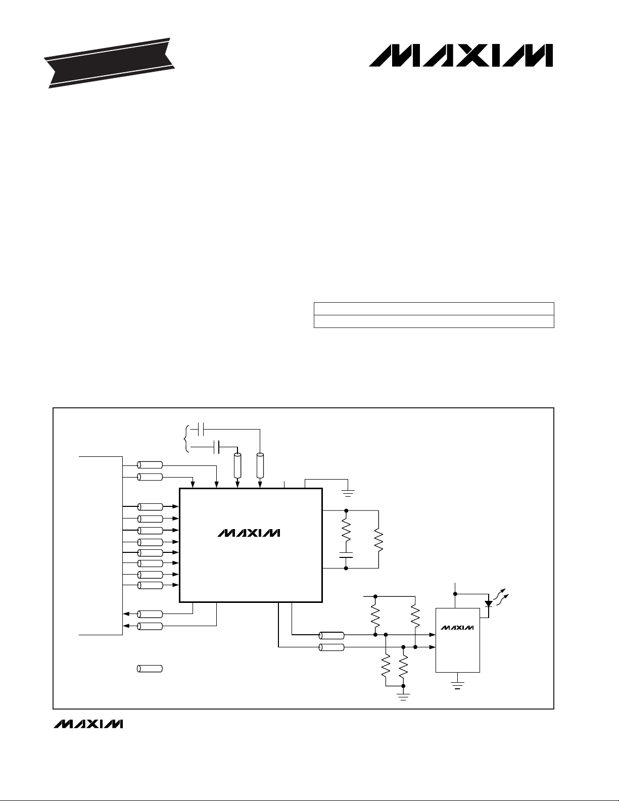
MAX3691
MAX3667
SD-PCLKO- PCLKO+
LVDS CRYSTAL REFERENCE
PCLKI- PCLKI+ RCLK-
0.1µF
0.1µF
V
CC
GND
SD+
FIL-
FIL+
130Ω 130Ω
82Ω
1.5k
100pF
24.9k
82Ω
V
CC
= +3.3V
V
CC
= +3.3V
V
CC
= +3.3V
OVERHEAD
GENERATION
PD3-
PD3+
PD2-
PD2+
PD1-
PD1+
PD0-
PD0+
THIS SYMBOL REPRESENTS A TRANSMISSION LINE
OF CHARACTERISTIC IMPEDANCE (Z
0
= 50Ω)
RCLK+
___________________________________________________Typical Operating Circuit
19-1207; Rev 0; 3/97
PART
MAX3691ECJ -40°C to +85°C
TEMP. RANGE PIN-PACKAGE
32 TQFP
______________Ordering Information
For free samples & the latest literature: http://www.maxim-ic.com, or phone 1-800-998-8800
Pin Configuration appears at end of data sheet.
EVALUATION KIT
AVAILABLE
Page 2
MAX3691
+3.3V, 622Mbps, SDH/SONET 4:1 Serializer
with Clock Synthesis and LVDS Inputs
2 _______________________________________________________________________________________
ABSOLUTE MAXIMUM RATINGS
DC ELECTRICAL CHARACTERISTICS
(VCC= +3.0V to +3.6V, differential LVDS loads = 100Ω ±1%, PECL loads = 50Ω ±1% to (V
CC
- 2V), TA= -40°C to +85°C, unless
otherwise noted. Typical values are at V
CC
= +3.3V, TA= +25°C.)
Stresses beyond those listed under “Absolute Maximum Ratings” may cause permanent damage to the device. These are stress ratings only, and functional
operation of the device at these or any other conditions beyond those indicated in the operational sections of the specifications is not implied. Exposure to
absolute maximum rating conditions for extended periods may affect device reliability.
Terminal Voltage (with respect to GND)
V
CC
.........................................................................-0.5V to 5V
All Inputs.................................................-0.5V to (V
CC
+ 0.5V)
Output Current
LVDS Outputs (PCLKO±)................................................10mA
PECL Outputs (SD±).......................................................50mA
Continuous Power Dissipation (T
A
= +85°C)
TQFP (derate 10.20mW/°C above +85°C)...................663mW
Operating Temperature Range ...........................-40°C to +85°C
Storage Temperature Range.............................-65°C to +160°C
Lead Temperature (soldering, 10sec).............................+300°C
T
A
= +25°C to +85°C
PECL outputs unterminated
TA= +25°C to +85°C
Differential input voltage =
100mV
Common-mode voltage =
50mV
CONDITIONS
V
VCC- 1.03 VCC- 0.88
V
OH
Output High Voltage
mA38 65 100I
CC
Supply Current
V0.925V
OL
Output Low Voltage
V1.475V
OH
Output High Voltage
Ω
85 100 115R
IN
Differential Input Resistance
mV70V
HYST
Threshold Hysteresis
V
VCC- 1.81 VCC- 1.62
V
OL
Output Low Voltage
V0 2.4V
I
Input Voltage Range
mV-100 100V
IDTH
Differential Input Threshold
UNITSMIN TYP MAXSYMBOLPARAMETER
%±1 ±10
∆R
O
Change in Magnitude of Single-Ended Output
Resistance for Complementary States
Ω
40 70 140R
O
Single-Ended Output Resistance
mV25
∆V
OS
Change in Magnitude of Output Offset Voltage
for Complementary States
mV250 400V
OD
Differential Output Voltage
mV25
∆V
OD
Change in Magnitude of Differential Output
Voltage for Complementary States
TA= +25°C V1.125 1.275V
OS
Output Offset Voltage
PECL OUTPUTS (SD±)
LVDS INPUTS AND OUTPUTS (PCLKI±, RCLK±, PCLKO±, PD_±)
TA= -40°C VCC- 1.08 VCC- 0.88
TA= -40°C VCC- 1.95 VCC- 1.62
Page 3
MAX3691
+3.3V, 622Mbps, SDH/SONET 4:1 Serializer
with Clock Synthesis and LVDS Inputs
_______________________________________________________________________________________ 3
Note 1: AC characteristics guaranteed by design and characterization.
Note 2: Assumes a 50% duty cycle ±5%.
TA= -40°C to +85°C (Note 2)
CONDITIONS
ps600t
H
Parallel Data-Hold Time
ps200t
SU
MHz622.08f
SCLK
Serial Clock Rate
Parallel Data-Setup Time
ns-0.7 +3.3t
SKEW
PCLKO to PCLKI Skew
ps
RMS
13
Φ
0
Output Jitter
ps400t
R, tF
PECL Differential Output
Rise/Fall Time
UNITSMIN TYP MAXSYMBOLPARAMETER
AC ELECTRICAL CHARACTERISTICS
(VCC= +3.0V to +3.6V, differential LVDS load = 100Ω ±1%, PECL loads = 50Ω ±1% to (V
CC
- 2V) TA= +25°C, unless otherwise
noted. Typical values are at V
CC
= +3.3V.) (Note 1)
100
0
-50 -25 25 100
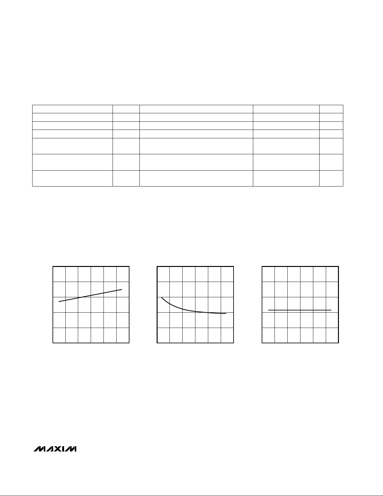
SUPPLY CURRENT
vs. TEMPERATURE
20
60
80
MAX3691-01
TEMPERATURE (°C)
SUPPLY CURRENT (mA)
0 504075
-20
-120
-50 -25 25 100
PARALLEL DATA-SETUP TIME
vs. TEMPERATURE
-100
-60
-40
MAX3691-02
TEMPERATURE (°C)
PARALLEL DATA-SETUP TIME (ps)
0 50
-80
75
250
150
-50 -25 25 100
PARALLEL DATA-HOLD TIME
vs. TEMPERATURE
170
210
230
MAX3691-03
TEMPERATURE (°C)
PARALLEL DATA-HOLD TIME (ps)
0 50
190
75
__________________________________________Typical Operating Characteristics
(V
CC
= +3.0V to +3.6V, differential LVDS loads = 100Ω, unless otherwise noted.)
Page 4

MAX3691
+3.3V, 622Mbps, SDH/SONET 4:1 Serializer
with Clock Synthesis and LVDS Inputs
4 _______________________________________________________________________________________
____________________________Typical Operating Characteristics (continued)
(V
CC
= +3.0V to +3.6V, differential LVDS loads = 100Ω, unless otherwise noted.)
6
-4
-50 -25 25 100
PCLKO-to-PCLKI SKEW
vs. TEMPERATURE
-2
2
4
MAX3691-04
TEMPERATURE (°C)
PCLKO-TO-PCLKI SKEW (ns)
0 50075
1.21V
0.59V
161ps/div
SERIAL-DATA OUTPUT EYE DIAGRAM
(622Mbps, 2
7
-1 PRBS)
62mV/
div
MAX3691-05
OC-12
SONET MASK
908mV
808mV
10ps/div
SERIAL-DATA OUTPUT JITTER
10mV/
div
MAX3691-06
f
RCLK
= 155.52MHz
Mean 23.88ns
RMS
∆ 8.418ps
PkPk 70.2ps
µ±1σ 68.774%
µ±2σ 95.534%
µ±3σ 99.738%
______________________________________________________________Pin Description
NAME FUNCTION
1, 3, 5, 7 PD0+ to PD3+ Noninverting LVDS Parallel Data Inputs. Data is clocked in on the PCLKI signal’s positive transition.
2, 4, 6, 8 PD0- to PD3- Inverting LVDS Parallel Data Inputs. Data is clocked in on the PCLKI signal’s positive transition.
PIN
9, 17, 18,
19, 24,
25, 32
GND Ground
10 PCLKO- Inverting LVDS Parallel-Clock Output. Use PCLKO to clock the overhead management circuit.
15 SD+ Noninverting PECL Serial-Data Output
14 SD- Inverting PECL Serial-Data Output
12, 13, 16,
20, 21,
28, 29
V
CC
+3.3V Supply Voltage
11 PCLKO+ Noninverting LVDS Parallel-Clock Output. Use PCLKO to clock the overhead management circuit.
23 FIL+ Filter Capacitor Input. See
Typical Operating Circuit
for external-component connections.
22 FIL- Filter Capacitor Input. See
Typical Operating Circuit
for external-component connections.
26 RCLK+
Noninverting LVDS Reference Clock Input. Connect (AC couple) a crystal reference clock
(155.52MHz) to the RCLK inputs.
30 PCLKI+
Noninverting LVDS Parallel Clock Input. Connect the incoming parallel-data-clock signal to the
PCLKI inputs. Note that data is updated on the positive transition of the PCLKI signal.
27 RCLK-
Inverting LVDS Reference Clock Input. Connect (AC couple) a crystal reference clock (155.52MHz)
to the RCLK inputs.
31 PCLKI-
Inverting LVDS Parallel Clock Input. Connect the incoming parallel-data-clock signal to the PCLKI
inputs. Note that data is updated on the positive transition of the PCLKI signal.
Page 5

MAX3691
+3.3V, 622Mbps, SDH/SONET 4:1 Serializer
with Clock Synthesis and LVDS Inputs
_______________________________________________________________________________________ 5
_______________Detailed Description
The MAX3691 serializer comprises a 4-bit parallel input
register, a 4-bit shift register, control and timing logic, a
PECL output buffer, LVDS input/output buffers, and a
frequency-synthesizing PLL (consisting of a phase/
frequency detector, loop filter/amplifier, and voltagecontrolled oscillator). This device converts 4-bit-wide,
155Mbps data to 622Mbps serial data (Figure 1).
The PLL synthesizes an internal 622Mbps reference
used to clock the output shift register. This clock is
generated by locking onto the external 155.52MHz
reference-clock signal (RCLK).
The incoming parallel data is clocked into the
MAX3691 on the rising transition of the parallel-clockinput signal (PCLKI). The control and timing logic
ensure proper operation if the parallel-input register is
latched within a window of time that is defined with
respect to the parallel-clock-output signal (PCLKO).
PCLKO is the synthesized 622Mbps internal serialclock signal divided by four. The allowable PCLKO-toPCLKI skew is -0.7ns to +3.3ns. This defines a timing
window at about the PCLKO rising edge, during which
a PCLKI rising edge may occur. Figure 2 is the timing
diagram.
MAX3691
PD3+
PD3-
4-BIT
PARALLEL
INPUT
REGISTER
PHASE/FREQ
DETECT
CONTROL
4-BIT
SHIFT
REGISTER
LVDS
LVDS
PCLKI-
PCLKI+
RCLK-
RCLK+
FIL+ FIL- PCLKO+ PCLKO-
VCO
PECL
SD+
SD-
SHIFT
LATCH
LVDS
PD2+
PD2-
LVDS
PD1+
PD1-
LVDS
PD0+
PD0-
LVDS
LVDS
Figure 1. Functional Diagram
Page 6

MAX3691
Low-Voltage Differential-Signal (LVDS)
Inputs and Outputs
The MAX3691 features LVDS inputs and outputs for
interfacing with high-speed digital circuitry. The LVDS
standard is based on the IEEE 1596.3 LVDS specification. This technology uses 250mV–400mV differential low-voltage swings to achieve fast transition
times, minimized power dissipation, and noise immunity.
For proper operation, the parallel-clock LVDS outputs
(PCLKO+, PCLKO-) require 100Ω differential DC termi-
nation between the inverting and noninverting outputs.
Do not terminate these outputs to ground.
The parallel data and parallel clock LVDS inputs (PD_+,
PD_-, PCLKI+, PCLKI-) are internally terminated with
100Ω differential input resistance, and therefore do not
require external termination.
PECL Outputs
The serial-data PECL outputs (SD+, SD-) require 50Ω
DC termination to (VCC- 2V). See the
Alternative PECL-
Output Termination
section.
+3.3V, 622Mbps, SDH/SONET 4:1 Serializer
with Clock Synthesis and LVDS Inputs
6 _______________________________________________________________________________________
t
SKEW
SD
NOTE: SIGNALS SHOWN ARE DIFFERENTIAL. FOR EXAMPLE, PCLKO = (PCLKO+) - (PCLKO-).
*PD3 = D3; PD2 = D2; PD1 = D1; PD0 = D0.
D0D1D2D3
PD_
VALID PARALLEL DATA*
PCLKI
PCLKO
t
SU
t
H
Figure 2. Timing Diagram
Page 7

___________________Chip Information
TRANSISTOR COUNT: 1633
MAX3691
+3.3V, 622Mbps, SDH/SONET 4:1 Serializer
with Clock Synthesis and LVDS Inputs
_______________________________________________________________________________________ 7
MAX3691
SD+
SD-
V
CC
- 2V
50Ω 50Ω
Z
0
= 50Ω
HIGHIMPEDENCE
INPUTS
Z0 = 50Ω
MAX3691
SD+
SD-
+3.3V
130Ω
130Ω
82Ω 82Ω
Z
0
= 50Ω
PECL
INPUTS
Z0 = 50Ω
Figure 3. Alternative PECL-Output Termination
TQFP
TOP VIEW
FIL+
FIL-
VCCVCCGND
GND
GND
GND
PD0-
PD1+
PD1-
PD2+
PD2-
PD0+
PD3-
PD3+
SD+
SD-
PCLKO-
V
CC
V
CC
PCLKO+
V
CC
GND
RCLK+
RCLK-
PCLKI-
V
CC
V
CC
PCLKI+
GND
GND
32
31
30
29
28
27
26
25
17
18
19
20
21
22
23
24
9
10
11
12
13
14
15
16
8
7
6
5
4
3
2
1
MAX3691
__________________Pin Configuration__________Applications Information
Alternative PECL-Output Termination
Figure 3 shows alternative PECL output-termination
methods. Use Thevenin-equivalent termination when a
(VCC- 2V) termination voltage is not available. If AC
coupling is necessary, be sure that the coupling capacitor is placed following the 50Ω or Thevenin-equivalent
DC termination.
Layout Techniques
For best performance, use good high-frequency layout
techniques. Filter voltage supplies and keep ground
connections short. Use multiple vias where possible.
Also, use controlled-impedance transmission lines to
interface with the MAX3691 clock and data inputs and
outputs.
Page 8

Maxim cannot assume responsibility for use of any circuitry other than circuitry entirely embodied in a Maxim product. No circuit patent licenses are
implied. Maxim reserves the right to change the circuitry and specifications without notice at any time.
8
___________________Maxim Integrated Products, 120 San Gabriel Drive, Sunnyvale, CA 94086 (408) 737-7600
© 1997 Maxim Integrated Products Printed USA is a registered trademark of Maxim Integrated Products.
MAX3691
+3.3V, 622Mbps, SDH/SONET 4:1 Serializer
with Clock Synthesis and LVDS Inputs
________________________________________________________Package Information
TQFPPO.EPS
 Loading...