

Page 1
For free samples & the latest literature: http://www.maxim-ic.com, or phone 1-800-998-8800.
For small orders, phone 408-737-7600 ext. 3468.
________________General Description
The MAX3532 is a programmable power amplifier for
use in upstream cable applications. The device outputs
up to 62dBmV (continuous wave) through a 1:2 (voltage
ratio) transformer when driven with 36dBmV at its input.
It features variable gain, which is controlled via a 3-wire
digital serial bus and available in 1dB steps. The operating frequency ranges from 5MHz to 42MHz.
The MAX3532 offers three operating modes: high power,
low noise, and transmit disable. High-power mode
achieves the highest output levels, while low-noise mode
achieves the lowest output noise when driving lower output levels. Transmit disable mode places the device in a
high-isolation state with minimum output noise, for use
between bursts in TDMA systems.
Two power-down modes are also available. Software shutdown mode permits power-down of all analog circuitry while
maintaining the programmed gain setting. Shutdown mode
disables all circuitry and reduces current consumption
below 10µA.
The MAX3532 comes in a 36-pin SSOP package screened
for the extended-industrial temperature range (-40°C to
+85°C).
________________________Applications
Cable Modems Telephony over Cable
CATV Set-Top Box
____________________________Features
♦ Single +5V Supply
♦ Output Level Ranges from Less than 8dBmV
to 62dBmV, in 1dB Steps
♦ Gain Programmable in 1dB Steps
♦ 350mW Typical Power Dissipation
♦ Transmit-Disable Mode
♦ Two Shutdown Modes
MAX3532
†
Upstream CATV Driver Amplifier
________________________________________________________________
Maxim Integrated Products
1
36
35
34
33
32
31
30
29
28
27
26
25
24
23
1
2
3
4
5
6
7
8
9
10
11
12
13
14
SHDN
TXEN
VOUTVOUT+
GND
V
EE
2
GND
V
CC
2
V
CC
VIN+
VINV
EE
GND
GND
V
CC
1
GND
GND
V
EE
1
GND
GND
GND
GND
GND
GND
GND
GND
GND
GND
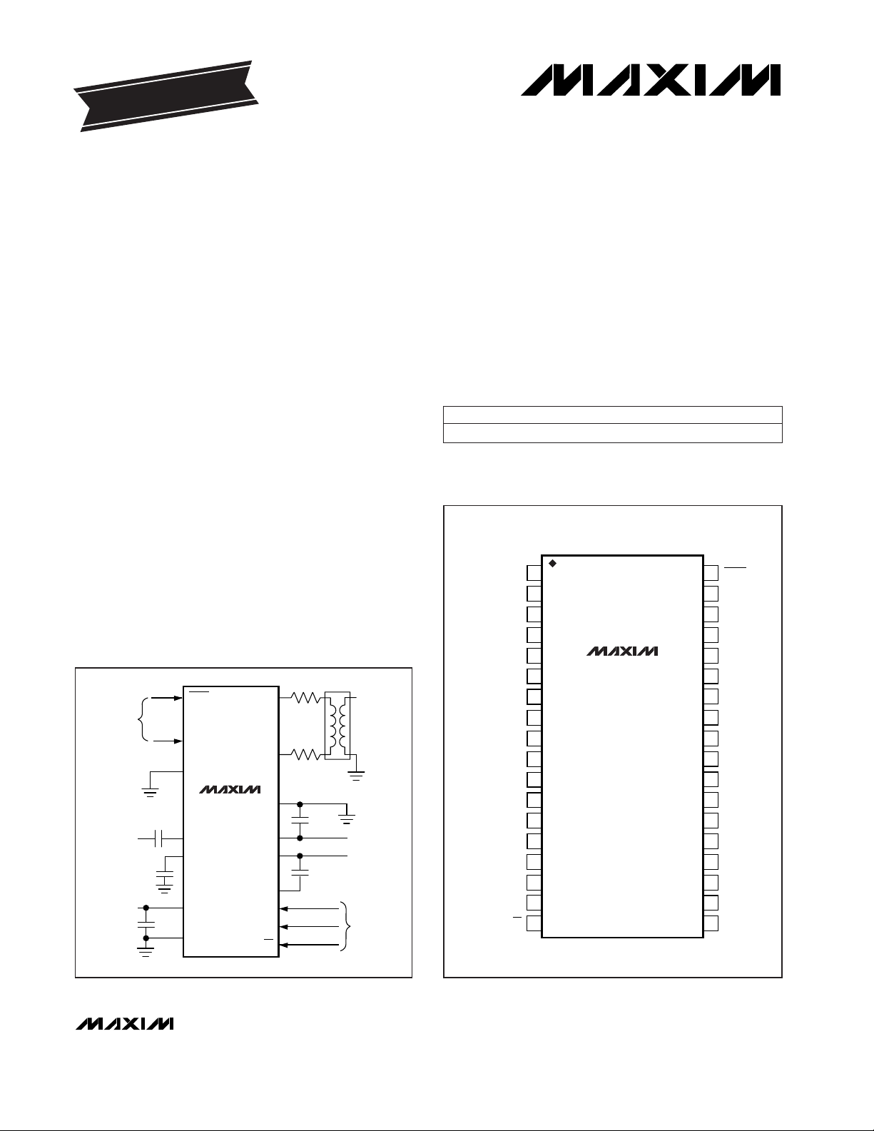
SSOP
TOP VIEW
MAX3532
22
21
20
19
15
16
17
18 SDA
GND
GND
SCLK
CS
GND
GND
GND
___________________Pin Configuration
MAX3532
VOUT-
CONTROL
LOGIC
INPUT
V
CC
VEE2
VOUT+
V
CC
2
V
CC
V
EE
SCLK
SDA
CS
34
31
33
30
29
26
20
19
18
SHDN OUTPUT
TXEN
0.001µF
0.001µF
0.1µF
0.1µF
8.0Ω
8.0Ω
1:2
0.1µF
VIN+
GND
VIN-
V
CC
1
V
EE
1
V
CC
V
CC
CONTROL
LOGIC
36
35
28
1–10, 12, 13, 15–17,
21–25, 32
27
14
11
__________Typical Operating Circuit
19-1331; Rev 1; 6/98
PART
MAX3532EAX -40°C to +85°C
TEMP. RANGE PIN-PACKAGE
36 SSOP
EVALUATION KIT
AVAILABLE
_______________Ordering Information
†
Protected under U.S. Patent 5,748,027
Page 2
MAX3532
†
Upstream CATV Driver Amplifier
2 _______________________________________________________________________________________
ABSOLUTE MAXIMUM RATINGS
DC ELECTRICAL CHARACTERISTICS
(VCC= +4.75V to +5.25V, no RF applied, TA= -40°C to +85°C, unless otherwise noted.)
Stresses beyond those listed under “Absolute Maximum Ratings” may cause permanent damage to the device. These are stress ratings only, and functional
operation of the device at these or any other conditions beyond those indicated in the operational sections of the specifications is not implied. Exposure to
absolute maximum rating conditions for extended periods may affect device reliability.
VCC........................................................................-0.5V to +7.0V
Input Voltage Levels (all inputs).................-0.3V to (V
CC
+ 0.3V)
Continuous RMS Input Voltage (VIN+, VIN-)..................60dBmV
Continuous Current (VOUT+, VOUT-)...............................100mA
Continuous Power Dissipation (T
A
= +70°C)
36-Pin SSOP (denote at 11mW/°C above +70°C) ........900mW
Operating Temperature Range ...........................-40°C to +85°C
Junction Temperature......................................................+150°C
Storage Temperature Range.............................-65°C to +165°C
Lead Temperature (soldering, 10sec).............................+300°C
TXEN = X, SHDN = 1, D7 and D6 = 00
TXEN = 1, SHDN = 1, D7 and D6 = 1X or 01
CS, SDA, SCLK, TXEN, SHDN
TXEN = X, SHDN = 0, D7 and D6 = XX
CS, SDA, SCLK, TXEN, SHDN
CS, SDA, SCLK, TXEN, SHDN
CS, SDA, SCLK, TXEN, SHDN
CONDITIONS
mA1.5 2I
CC
Software Shutdown Current
mA RMS75 95I
CC
V4.75 5.25V
CC
Supply Voltage
Supply Current
µA-100I
IL
Digital Input Low Current
µA0.1 10I
CC
Shutdown Current
V2.4V
IH
Digital Input High Voltage
V0.8V
IL
Digital Input Low Voltage
µA100I
IH
Digital Input High Current
UNITSMIN TYP MAXSYMBOLPARAMETER
D7 and D6 = 11, BW = 160kHz,
V
OUT
= 46dBmV to 62dBmV, f = 5MHz to 42MHz
VIN= 36dBmV to 40dBmV, AV= 22dB
VIN= 36dBmV to 40dBmV, AV= 22dB
fIN= 20MHz, V
OUT
= 58dBmV
fIN= 20MHz, V
OUT
= 52dBmV
Two input tones at 40MHz and 40.25MHz, both at
30dBmV; V
OUT
= 52dBmV per tone
TXEN = 0, fIN= 42MHz, V
OUT
= 58dBmV
CONDITIONS
dBc-80 -79
Output Noise
(High-Power Mode) (Note 1)
degrees1AMPMAM to PM
dB0.1AMAMAM to AM
dBc
-46 -40
HD2
-59 -55
Second Harmonic Distortion
(Note 1)
dBc-43 -37.5IMR3
Two-Tone Third-Order
Distortion (Note 1)
dB36Isolation in Standby Mode
dB1Output Step Size
dB
-32 -28
A
V
Voltage Gain
24 26
Vp-p3.6V
TXOUT
Output Signal Swing
UNITSMIN TYP MAXSYMBOLPARAMETER
AC ELECTRICAL CHARACTERISTICS
(VCC= +5V, VIN= 36dBmV, SHDN = TXEN = 1, fIN= 20MHz, Z
LOAD
= 75Ω through a 1:2 transformer with two precision 8.0Ω back-
termination resistors, T
A
= -40°C to +85°C, unless otherwise noted. Typical values are measured at TA= +25°C.)
fIN= 14MHz, V
OUT
= 58dBmV
fIN= 14MHz, V
OUT
= 52dBmV
dBc
-57 -48
HD3
-67 -58
Third Harmonic Distortion
(Note 1)
High power, D7–D0 = 11111101
Low noise, D7–D0 = 1001000
Page 3
Output Noise
(Standby Mode) (Note 1)
MAX3532
†
Upstream CATV Driver Amplifier
_______________________________________________________________________________________ 3
Note 1: Guaranteed by design and characterization.
AC ELECTRICAL CHARACTERISTICS (continued)
(VCC= +5V, VIN= 36dBmV, SHDN = TXEN = 1, fIN= 20MHz, Z
LOAD
= 75Ω through a 1:2 transformer with two precision 8.0Ω back-
termination resistors, T
A
= -40°C to +85°C, unless otherwise noted. Typical values are measured at TA= +25°C.)
SCLK Pulse Width High t
SCLKH
50
SCLK Pulse Width Low t
SCLKL
ns(Note 1)
50 ns(Note 1)
SDA to SCLK Setup Time t
SDAS
20
SDA to SCLK Hold Time t
SDAH
ns(Note 1)
20 ns(Note 1)
PARAMETER SYMBOL MIN TYP MAX UNITS
Output Noise
(Low-Power Mode)
(Note 1)
-75 -73 dBc
Output Return Loss (Note 1) 12 dB
TXEN Transient Duration 3 7 µs
TXEN Transient Step Size 25 100 mV
Power-Enable Transient
Duration (Note 1)
1 2.5 5 µs
CS to SCLK Setup Time
t
CSS
20
CONDITIONS
TXEN rise/fall time < 100ns, TA= +25°C (Note 1)
ns
TA= +25°C, AV= 22dB (Note 1)
D7 and D6 = 10, V
OUT
> 27dBmV,
BW = 160kHz, f = 5MHz to 42MHz
fIN= 5MHz to 42MHz
TA= +25°C
(Note 1)
CS to SCLK Hold Time
t
CSH
20 ns(Note 1)
Output Noise
(Standby Mode) (Note 1)
-47 -45 dBmV
TXEN = 0, BW = 160kHz,
f = 5MHz to 42MHz
-47 -45 dBmV
D7 and D6 = 10, V
OUT
≤ 27dBmV,
BW = 160kHz, f = 5MHz to 42MHz
SERIAL INTERFACE
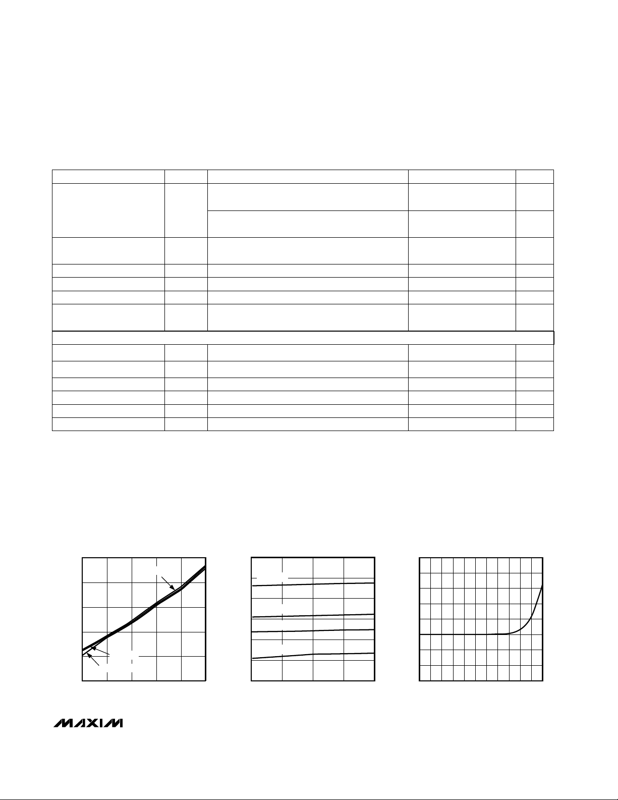
__________________________________________Typical Operating Characteristics
(VCC= 5.0V, VIN= 36dBmV, fIN= 20MHz, SHDN = TXEN = 1, Z
LOAD
= 75Ω through a 1:2 transformer with two precision 8.0Ω back-
termination resistors, T
A
= +25°C, unless otherwise noted.)
60
65
75
70
80
85
-40 0-20 25 50 85
SUPPLY CURRENT vs. TEMPERATURE
MAX3532toc01
TEMPERATURE (°C)
SUPPLY CURRENT (mA)
VCC = 5.25V
VCC = 4.75V
VCC = 5.0V
60
70
65
80
75
85
90
4.75 5 5.25
SUPPLY CURRENT vs. SUPPLY VOLTAGE
MAX3532toc02
SUPPLY VOLTAGE (V)
SUPPLY CURRENT (mA)
TA = +85°C
TA = +25°C
TA = 0°C
TA = -40°C
60
65
95
75
70
80
85
90
100
12 21 26 3116 36 41 5550 5945 64
SUPPLY CURRENT vs. OUTPUT LEVEL
MAX3532toc03
OUTPUT LEVEL (dBmV)
SUPPLY CURRENT (mA)
Page 4

MAX3532
†
Upstream CATV Driver Amplifier
4 _______________________________________________________________________________________
_____________________________Typical Operating Characteristics (continued)
(VCC= +5V, VIN= 36dBmV, SHDN = TXEN = 1, fIN= 20MHz, Z
LOAD
= 75Ω through a 1:2 transformer with two precision 8.0Ω back-
termination resistors, T
A
= -40°C to +85°C, unless otherwise noted. Typical values are measured at TA= +25°C.)
-40
-20
-30
0
57
-10
10
20
30
40
0 40 6020 80 100 120 140
GAIN vs. FREQUENCY
MAX3532toc04
FREQUENCY (MHz)
GAIN (dB)
HIGH-POWER MODE
LOW-NOISE MODE
18
24
30
36
42
48
54
60
48
54
GAIN STATE 60
-50
-45
-15
-35
-40
-30
-25
-20
-10
5 15 20 2510 30 35 5045 5540 60
OUTPUT NOISE vs. GAIN STATE
MAX3532toc05
GAIN STATE
OUTPUT NOISE IN 160kHz (dBmV)
LOW-NOISE MODE
HIGH-POWER MODE
-10
20
10
0
30
40
60
50
70
0 10 155 20 25 30 35 40 45 50 55 60
OUTPUT LEVEL vs. GAIN STATE
MAX3532toc06
GAIN STATE
OUTPUT LEVEL (dBmV)
LOW-NOISE MODE
HIGH-POWER MODE
-6000
-2000
-4000
4000
2000
0
10,000
8000
6000
12,000
0 4020 60 80 100
REAL AND IMAGINARY INPUT
IMPEDANCE vs. FREQUENCY
MAX3532toc07
FREQUENCY (MHz)
IMPEDANCE (Ω)
REAL
IMAGINARY
-70
-60
-65
-50
-55
-45
-40
-35
-30
10 20 2515 30 35 40 45 50
SECOND HARMONIC DISTORTION vs.
INPUT FREQUENCY
MAX3532toc09
INPUT FREQUENCY (MHz)
HARMONIC DISTORTION (dBc)
V
OUT
= 55dBmV
V
OUT
= 25dBmV
V
OUT
= 40dBmV
0
40
20
80
60
100
120
5 30 4010 20 50 75 100
REAL AND IMAGINARY OUTPUT
IMPEDANCE vs. FREQUENCY
MAX3532toc08
FREQUENCY (MHz)
IMPEDANCE (Ω)
REAL
IMAGINARY
-75
-65
-70
-50
-55
-60
-35
-40
-45
-30
10 25 3015 20 35 40 45 50
THIRD HARMONIC DISTORTION vs.
INPUT FREQUENCY
MAX3532toc10
INPUT FREQUENCY (MHz)
HARMONIC DISTORTION (dBc)
V
OUT
= 52dBmV
V
OUT
= 55dBmV
V
OUT
= 25dBmV
V
OUT
= 40dBmV
Page 5

MAX3532
†
Upstream CATV Driver Amplifier
_______________________________________________________________________________________ 5
______________________________________________________________Pin Description
NAME FUNCTION
1–10, 12, 13,
15, 16, 17,
21–25, 32
GND Ground Pins
11 VEE1
Serial Data Interface Ground. As with all grounds, maintain the shortest possible
(low-inductance) connections to the ground plane.
PIN
14 VCC1
Serial Data Interface +5V Supply. Bypass this pin with a 0.1µF decoupling capacitor as close to the
part as possible.
18
CS
Serial-Interface Enable. TTL-compatible input. See
Serial Interface
section.
27 VIN-
Negative Input. When not used, this port must be AC coupled to ground. Along with VIN+, this port
forms a high-impedance differential input to the PGA. Driving this port differentially will increase the
rejection of second-order distortion.
26 V
EE
Programmable Gain Amplifier (PGA) Ground. As with all grounds, maintain the shortest possible
(low-inductance) connection to the ground plane.
20 SCLK Serial-Interface Clock. TTL-compatible input. See
Serial Interface
section.
19 SDA Serial-Interface Data. TTL-compatible input. See
Serial Interface
section.
33 VOUT+
Positive Output. Along with VOUT-, this pin forms a low-impedance output. Typically this port drives
a 1:2 transformer through 8Ω series resistors.
31 VEE2
Power Amplifier Ground. As with all grounds, connections maintain the shortest possible (low-inductance) length to the ground plane.
30 VCC2
Power Amplifier +5V Supply. Bypass this pin with a decoupling capacitor as close to the part as
possible.
29 V
CC
PGA +5V Supply. Bypass this pin with a decoupling capacitor as close to the part as possible.
28 VIN+
Positive Input. Along with VIN-, this port forms a high-impedance differential input to the PGA. Driving
this port differentially will increase the rejection of second-order distortion. AC couple to this pin.
36
SHDN
Shutdown. When this pin is set low, all functions (including the serial interface) are disabled, leaving
only leakage currents to flow.
35 TXEN
Transmit Amplifier Enable. Setting this pin low places the transmitter in a high-isolation state (transmit
disable mode). In this mode, however, significant common-mode voltage swings exist. It is, therefore, important to maintain good balance of the differential output through to the transformer primary.
34 VOUT-
Negative Output. Along with VOUT+, this pin forms a low-impedance output. Typically this port
drives a 1:2 transformer through 8Ω series resistors.
Page 6

MAX3532
†
_______________Detailed Description
The following sections describe the blocks shown in the
Functional Diagram (Figure 1).
Programmable-Gain Amplifier
The MAX3532’s processing path is made up of the programmable-gain amplifier (PGA) and the transmit
power amplifier, which together provide better than
64dB of output level control in 1dB steps.
The PGA is implemented as a programmable Gilbert
cell attenuator. It uses a differential architecture to
achieve maximum linearity. When it is driven single
ended, specified performance is achieved given that
the unused input is decoupled to ground. The gain of
the PGA is determined by the serial-data interface. See
Table 2.
Transmit Power Amplifier
The transmit power amp is capable of driving +8dBmV
to +62dBmV differentially when driven with +36dBmV. To
achieve the necessary swing from a single +5V supply,
an external 1:2 transformer must be used. The output of
the transmit power amplifier is a very low-impedance
emitter follower, which requires two 8Ω series termination
resistors to achieve adequate output return loss.
The power amplifier’s gain is set via the serial-data
interface. The transmit power amplifier has a switchable
+16dB or +0dB gain to achieve high linearity or low
noise, respectively. High-gain mode sets the power
amp’s gain to +16dB, allowing for the highest output
signal swings. Low-noise mode sets the gain to 0dB,
which achieves the lowest output noise.
Shutdown Mode
In normal operation the shutdown pin (SHDN) is driven
high. When SHDN is asserted low, all circuits within the
IC are disabled. Only leakage currents flow in this
state. Data stored within the serial-data interface latches will be lost upon shutting down the part.
Transmit-Disable Mode
When the TXEN pin is asserted high, the device is in
transmit mode. When TXEN is driven low, the transmit
amplifier switches to common-mode operation and the
output signal appears at the output pins VOUT+ and
VOUT- with the same phase. These identical signals
cancel within the output transformer core, providing
high isolation from input to output. Optimum isolation is
achieved in low-noise mode with a low gain setting.
Serial Interface
The serial interface has an active-low enable (CS) to
bracket the data, with data clocked in MSB first on the
rising edge of SCLK. Data is stored in the storage latch
on the rising edge of CS. The serial interface controls
the state of the PGA and output amplifier. The register
format is shown in Tables 1 and 2. Serial-interface timing is shown in Figure 2.
Transmit Modes
The hardware TXEN line is ANDed with software bit D7,
so both TXEN and D7 must be high to transmit. Bit D6
governs whether the device is set to high-gain mode (D6
= 1) or to low-noise mode (D6 = 0). High-power mode
should be used for output levels above 45dBmV. This
transition point optimizes the MAX3532’s distortion performance, but either mode may be used throughout the full
complement of programmed gain states. Bits D5–D0
define 64 PGA gain states, nominally 1dB each.
Upstream CATV Driver Amplifier
6 _______________________________________________________________________________________
MAX3532
VOUT-
VIN+
PGA
SHDN
VIN-
CS
SDA SCLK
VOUT+
TXEN
SERIAL-DATA INTERFACE
BIAS
Figure 1. Functional Diagram
BIT MNEMONIC DESCRIPTION
MSB 7 D7 Chip-State Control MSB
6 D6 Chip-State Control LSB
5 D5 Gain Control, Bit 5
4 D4 Gain Control, Bit 4
3 D3 Gain Control, Bit 3
2 D2 Gain Control, Bit 2
1 D1 Gain Control, Bit 1
LSB 0 D0 Gain Control, Bit 0
Table 1. Serial-Interface Control Words
Page 7

Software Shutdown Mode
Software-shutdown mode is enabled when both D7 and
D6 are low (D7, D6 = 00). This mode minimizes current
consumption while maintaining the programmed gain
state stored in the serial data-interface’s latch. All analog functions are disabled in this mode.
__________Applications Information
Output Match
The MAX3532’s output circuit is a differential emitter follower that has a near-zero impedance over the operating frequency range. In order to match to a singleended impedance, a transformer and back-termination
resistors are required. Furthermore, operation from a
single +5V supply requires that the output signal swing
be stepped up to achieve the rated output levels.
These are described in the next two sections.
Transformer
To achieve the rated output levels, a 1:2 (voltage ratio)
transformer is required. This transformer must have
adequate bandwidth to cover the intended application.
Note that most RF transformers specify a bandwidth
with a 50Ω load on the primary and a matching resistance on the secondary winding. The much lower
(approximately 16Ω due to the back-termination resistors) impedance of the MAX3532’s output will tend to
shift the low-frequency edge of the bandwidth specification down by a factor of three or more due to primary
inductance. Keep this in mind when specifying a transformer.
RF transformer cores are inherently nonlinear devices,
which must be operated in their linear region if distortion is a critical consideration. In general, the size of the
transformer core used and the number of turns will govern the distortion performance of the transformer for a
given output level. Therefore a transformer of adequate
size must be used to minimize its contribution to the
overall distortion budget.
Back-Termination Resistors
The value of the back-termination resistors depends on
two parameters: the ultimate output impedance (as
referred through the output transformer), and the quality of the output match desired. The output impedance
depends on the value of the termination resistors by the
following formula:
Z
OUT
= 4 x [ 2 x (R
term
+ RP)]
where R
term
is the value of one termination resistor and
RPis parasitic resistance.
MAX3532
†
Upstream CATV Driver Amplifier
_______________________________________________________________________________________ 7
Table 2. Chip-State Control Bits
TXEN D5 D4 D3 D2 D1 D0 STATE
1 X X X X X X High-power transmit
1 X X X X X X Low-noise transmit; subtract 16dB from V
OUT
X
X X X X X X X All analog circuitry off
1 0 0 1 1 0 1 V
OUT
= +8dBmV
1 0 0 1 1 1 0 V
OUT
= +9dBmV
— — — — — — — —
1 1 1 0 1 0 1 V
OUT
= +56dBmV
1 1 1 0 1 1 0 V
OUT
= +57dBmV
Figure 2. Serial-Interface Timing Diagram
D7
1
1
0
0
1
1
1
1
1
D6
1
0
1
0
0
0
—
1
1
*
Except state 000XXXXXX, which is software shutdown.
0* X
X X X X X X Transmit disabled
X
A B C D E F
D7 D6 D5 D4 D3 D2 D1 D0
A: t
CSS
B: t
SDAS
C: t
D: t
SDAH
SCKL
E: t
SCKH
F: t
CSH
Page 8

MAX3532
†
Upstream CATV Driver Amplifier
8 _______________________________________________________________________________________
Some allowance must be made for parasitic inductance
in the transformer as well as on the printed circuit
board. Therefore, choose a resistance value lower than
a perfect match. Two 8.0Ω resistors will provide a nearoptimum match.
If the output match is less than critical, the back-termination resistors can be set to a lower value. This will extend
the upper limit of the output level range (by dropping less
voltage across the resistors and more across the load),
and may improve distortion performance for a given output level.
Layout Issues
A well designed printed circuit board is an essential
part of an RF circuit. For best performance pay attention to power-supply layout issues, as well the output
circuit layout.
Output Circuit Layout
The differential implementation of the MAX3532’s output has the benefit of significantly reducing even-order
distortion, the most significant of which is second-harmonic distortion. The degree of distortion cancellation
depends on the amplitude and phase balance of the
overall circuit. It is critical that the traces leading from
the output pins be exactly the same length.
Since the MAX3532 has a low-impedance output, the
output traces must also be kept as short as possible,
as small amounts of inductance can have an impact at
higher frequencies. The back-termination resistors
should be kept as close to the device as possible.
Power-Supply Layout
For minimal coupling between different sections of the
IC, the ideal power-supply layout is a star configuration.
This configuration has a large valued decoupling
capacitor at the central VCCnode. The VCCtraces
branch out from this node, each going to a separate
VCCnode in the MAX3532 circuit. At the end of each of
these traces is a decoupling capacitor that provides a
very low impedance at the frequency of interest. This
arrangement provides local VCCdecoupling at each
VCCpin.
The traces leading from the supply to VCC(pin 29) and
VCC2 (pin 30) must be made as thick as practical to
keep resistance well below 1Ω.
Ground inductance degrades distortion performance.
Therefore, ground plane connections to VEE(pin 26)
and V
EE2
(pin 31) should be made with multiple vias if
possible.
Chip Information
TRANSISTOR COUNT: 1100
________________________________________________________Package Information
SSOP2.EPS
 Loading...