

Page 1
19-0453; Rev 0; 1/96
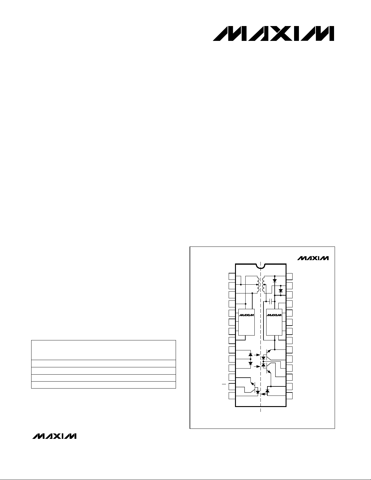
Complete, Isolated, 3.3V
RS-485/RS-422 Data Interface
_______________General Description
The MAX3480A/MAX3480B are electrically isolated
RS-485/RS-422 data-communications interfaces.
Transceivers, optocouplers, and a transformer are all
included in one low-cost, 28-pin DIP package. A single
+3.3V supply on the logic side powers both sides of the
interface.
The MAX3480B features reduced-slew-rate drivers that
minimize EMI and reduce reflections caused by
improperly terminated cables, allowing error-free data
transmission at data rates up to 250kbps. The
MAX3480A’s driver slew rate is not limited, allowing
transmission rates up to 2.5Mbps.
These devices typically draw 180mA of quiescent supply current. The MAX3480B provides a low-power shutdown mode in which it consumes only 0.2µA.
Drivers are short-circuit current limited and are protected against excessive power dissipation by thermal
shutdown circuitry that places the driver outputs into a
high-impedance state. The receiver input has a fail-safe
feature that guarantees a logic-high output if the input
is open circuit.
The MAX3480A/MAX3480B typically withstand 1600V
(1 minute) or 2000V
(1 second). Their isolated inputs
RMS
RMS
and outputs meet RS-485/RS-422 specifications.
________________________Applications
Isolated RS-485/RS-422 Data Interface
Transceivers for EMI-Sensitive Applications
Industrial-Control Local Area Networks
Automatic Test Equipment
HVAC/Building Control Networks
______________Ordering Information
DATA
PART
MAX3480ACPI
MAX3480AEPI
MAX3480BCPI
MAX3480BEPI -40°C to +85°C 28 Plastic DIP
TEMP. RANGE PIN-PACKAGE
0°C to +70°C
-40°C to +85°C
0°C to +70°C
28 Plastic DIP
28 Plastic DIP
28 Plastic DIP
RATE
(kbps)
2500
2500
250
250
____________________________Features
♦ Isolated Data Interface to 1600V
♦ Slew-Rate-Limited Data Transmission (MAX3480B)
♦ High-Speed, Isolated, 2.5Mbps RS-485 Interface
(MAX3480A)
♦ -7V to +12V Common-Mode Input Voltage Range
with Respect to Isolated Ground
♦ Single +3.3V Supply
♦ Current Limiting and Thermal Shutdown for
Driver Overload Protection
♦ Standard 28-Pin DIP Package
RMS
(1 minute)
__________________Pin Configuration
TOP VIEW
MAX3480A/B
V
CC1
V
CC2
GND1
CC3
V
CC4
GND2
V
CC5
1
2
D1
3
D2
4
5
MAX845
6
FS
SD
7
8
DI
9
10
DE
11
12
RO
13
14
MAX485
MAX487
28
27
26
25
24
23
22
21
20
19
18
17
16
15
AC1
AC2
ISO V
CC1
B
ISO RO DRV
A
ISO DI IN
ISO DE INV
ISO COM1
ISO DI DRV
ISO V
CC2
ISO DE DRV
ISO COM2
ISO RO LED
MAX3480A/MAX3480B
ISOLATION BARRIER
DIP
________________________________________________________________
Maxim Integrated Products
1
For free samples & the latest literature: http://www.maxim-ic.com, or phone 1-800-998-8800
Page 2

Complete, Isolated, 3.3V
RS-485/RS-422 Data Interface
ABSOLUTE MAXIMUM RATINGS
With Respect to GND:
V
V
V
Supply Voltage (V
Supply Voltage (V
CC
CC
2,
CC
1,
) ..........................................-0.3V to +7V
CC3
Control Input Voltage (SD, FS)................-0.3V to (V
Receiver Output Voltage (RO
).................-0.3V to (VCC+ 0.3V)
).........-0.3V to +3.8V
CC
4,
5
CC
+ 0.3V)
With Respect to ISO COM:
Control Input Voltage (ISO DE _) .........-0.3V to (ISO V
Driver Input Voltage (ISO DI _).........-0.3V to (ISO V
Receiver Output Voltage (ISO RO _)......-0.3V to (ISO V
CC
CC
CC
+ 0.3V)
+ 0.3V)
+ 0.3V)
Driver Output Voltage (A, B)................................-8V to +12.5V
Receiver Input Voltage (A, B)..............................-8V to +12.5V
Stresses beyond those listed under “Absolute Maximum Ratings” may cause permanent damage to the device. These are stress ratings only, and functional
operation of the device at these or any other conditions beyond those indicated in the operational sections of the specifications is not implied. Exposure to
absolute maximum rating conditions for extended periods may affect device reliability.
ELECTRICAL CHARACTERISTICS
(VCC= V
= V
V
CC
MAX3480A/MAX3480B
Switch Frequency
Operating Supply Current
FS Input Threshold
FS Input Pull-Up Current
FS Input Leakage Current
Input High Voltage
Input Low Voltage
Isolation Resistance
Isolation Capacitance
Differential Driver Output (no load) V
Differential Driver Output (with load)
CC1
CC1
= V
= V
CC2
CC2
= V
= V
CC4
CC4
= V
= 3.0V to 3.6V, FS = 0V, TA= T
CC5
= V
= 3.3V and TA= +25°C.) (Notes 1, 2, 3)
CC5
V
S
f
SWL
f
SWH
FS = 0V
FS = VCCor open
MAX3480A,
= VCCor open
DE
I
CC
I
SHDN
FSH
FSL
FSL
FSM
ISO
ISO
V
OD1
IH
IL
´
MAX3480B,
= V
DE
´
SD = V
High
Low
FS low
FS high
DE´, DI´(Figure 1)
DE´, DI´(Figure 1)
TA= +25°C, V
TA= +25°C, V
R = 50Ω (RS-422)
V
OD2
R = 27Ω (RS-485), Figure 3 1.5 5
CC
CC3
LED Forward Current (DI, DE, ISO RO LED) ......................50mA
Continuous Power Dissipation (TA= +70°C)
Plastic DIP (derate 9.09mW/°C above +70°C)...............727mW
Operating Temperature Ranges
MAX3480_CPI......................................................0°C to +70°C
MAX3480_EPI...................................................-40°C to +85°C
Storage Temperature Range.............................-65°C to +160°C
Lead Temperature (soldering, 10sec).............................+300°C
to T
MIN
, unless otherwise noted. Typical values are at
MAX
CONDITIONS
3.0 3.3 3.6Supply Voltage
600
900
180 260
280
120 200
240
or open
RL= ∞
RL= 54Ω
RL= ∞
RL= 54Ω
2.4V
0.8V
- 0.4V
CC
= 50V
ISO
ISO
= 50V
DC
DC
8
2
UNITSMIN TYP MAXSYMBOLPARAMETER
V
kHz
mA
µAShutdown Supply Current (Note 3) 0.2
V
µA50I
pA10I
VV
V0.4V
MΩ100 10,000R
pF10C
V
Change in Magnitude of Driver
Output Voltage for Complementary
Output States
Driver Common-Mode Output V
∆V
R = 27Ω or 50Ω,
OD
Figure 3
R = 27Ω or 50Ω, Figure 4
OC
Differential
2 _______________________________________________________________________________________
0.3
0.3Common Mode
4
V
V
Page 3
Complete, Isolated, 3.3V
RS-485/RS-422 Data Interface
ELECTRICAL CHARACTERISTICS (continued)
(VCC= V
= V
V
CC
Input Current (A, B)
Receiver Input Hysteresis
Receiver Output/Receiver Output
Low Voltage
Receiver Output/Receiver Output
High Current
Driver Short-Circuit Current
CC1
CC1
= V
= V
CC2
CC2
= V
= V
CC4
CC4
= V
= 3.0V to 3.6V, FS = 0V, TA= T
CC5
= V
= 3.3V and TA= +25°C.) (Notes 1, 2, 3)
CC5
IN
IN
TH
TH
OL
OSD
DE´= 0V,
= 0V or 3.6V
V
CC
-7V ≤ VCM≤ 12V
-7V ≤ VCM≤ 12V -0.2 0.2V
VCM= 0V
DI´= V
V
= 3.6V, DI´= 0V
OUT
-7V ≤ VO≤ 12V (Note 4) mA100ISO I
ISO I
R
OH
CONDITIONS
CC
SWITCHING CHARACTERISTICS—MAX3480A
(VCC= V
= V
V
CC
Driver Input to Output
Propagation Delay
Driver Output Skew (Note 5)
Driver Rise or Fall Time
Driver Enable to Output High
Driver Enable to Output Low
Driver Disable Time from High
Driver Disable Time from Low
Receiver Input to Output
Propagation Delay
t
PLH - tPHL
Receiver Skew
Maximum Data Rate
= V
CC1
= V
CC1
PARAMETER SYMBOL MIN TYP MAX UNITS
CC2
= V
CC2
Differential
= V
CC4 =VCC5
= V
CC4
= 3.0V to 3.6V, FS = 0V, TA= T
= 3.3V and TA= +25°C.)
CC5
t
PLH 100 275
t
PHL 100 275
t
SKEW 25 90 ns
tR, t
t
ZH 0.2 1.5 µs
t
t
HZ 0.3 1.5 µs
t
t
PLH
t
PHL
t
SKD
f
MAX 2.5 Mbps
Figures 4, 6; R
CL1= CL2= 100pF
Figures 4, 6; R
CL1= CL2= 100pF
Figures 4, 6; R
F 15 40 ns
CL1= CL2= 100pF
Figures 5, 7; CL= 100pF, S2 closed
ZL 0.2 1.5 µs
Figures 5, 7; CL= 100pF, S1 closed
Figures 5, 7; CL= 15pF, S2 closed
LZ 0.3 1.5 µsFigures 5, 7; C
Figures 4, 8; R
CL1= CL2= 100pF
Figures 4, 8; R
CL1= CL2= 100pF
t
PLH, tPHL < 50% of data period
CONDITIONS
DIFF
DIFF
DIFF
L
DIFF
DIFF
to T
MIN
MAX3480A
MAX3480B
MAX3480A
, unless otherwise noted. Typical values are at
MAX
VIN= 12V
VIN= 12V
VIN= -7V
VIN= 12V
VIN= -7V
12
MAX3480B 48
MIN
to T
, unless otherwise noted. Typical values are at
MAX
= 54Ω,
= 54Ω,
= 54Ω,
= 15pF, S1 closed
= 54Ω,
= 54Ω,
1.0
0.8
-0.8
0.25
-0.2
70∆V
100 225
100 225
20
MAX3480A/MAX3480B
UNITSMIN TYP MAXSYMBOLPARAMETER
mA
kΩReceiver Input Resistance
VReceiver Differential Threshold
mV
V0.4V
µA250I
ns
ns
ns
_______________________________________________________________________________________ 3
Page 4
Complete, Isolated, 3.3V
RS-485/RS-422 Data Interface
SWITCHING CHARACTERISTICS—MAX3480B
(VCC= V
= V
V
CC
Driver Input to Output
Propagation Delay
Driver Output Skew t
Driver Rise or Fall Time tR, t
Driver Enable to Output High t
Driver Enable to Output Low t
Driver Disable Time from Low t
Driver Disable Time from High t
Receiver Input to Output
Propagation Delay
t
PLH
MAX3480A/MAX3480B
Receiver Skew
Maximum Data Rate f
Note 1: All currents into device pins are positive; all currents out of device pins are negative. All voltages are referenced to
Note 2: For DE
Note 3: Shutdown supply current is the current at V
Note 4: Applies to peak current. See
= V
CC1
= V
CC1
PARAMETER SYMBOL MIN TYP MAX UNITS
- t
PHL
logic-side ground (GND1, GND2), unless otherwise specified.
MAX3480A/MAX3480B).
= V
CC2
CC2
Differential
and DI´pin descriptions, see
´
= V
CC4
CC4 =VCC5
= V
= 3.0V to 3.6V, FS = 0V, TA= T
= 3.3V and TA= +25°C.)
CC5
Typical Operating Characteristics
t
PLH
t
PHL
SKEW
ZH
HZ
t
PLH
t
PHL
t
SKD
MAX
Figures 4, 6; R
CL1= CL2= 100pF
Figures 4, 6; R
CL1= CL2= 100pF
Figures 4, 6; R
F
CL1= CL2= 100pF
Figures 5, 7; CL= 100pF, S2 closed
Figures 5, 7; CL= 100pF, S1 closed
ZL
Figures 5, 7; CL= 15pF, S1 closed
LZ
Figures 4, 8; R
CL1= CL2= 100pF
Figures 4, 8; R
CL1= CL2= 100pF
, t
PLH
PHL
Detailed Block Diagram
when shutdown is enabled.
CC1
to T
MIN
CONDITIONS
= 54Ω,
DIFF
= 54Ω,
DIFF
= 54Ω,
DIFF
= 54Ω,
DIFF
= 54Ω,
DIFF
< 50% of data period
and
and
MAX
Typical Application Circuit
Applications Information
, unless otherwise noted. Typical values are at
1.0 2.0
1.0 2.0
100 800 ns
1.0 2.0 µs
50 100 µs
50 100 µs
13 50 µs
13 50 µsFigures 5, 7; CL= 15pF, S2 closed
0.8 2.0
0.8 2.0
50
0.25 Mbpst
(Figure 1 for
.
µs
µs
ns
4 _______________________________________________________________________________________
Page 5
Complete, Isolated, 3.3V
RS-485/RS-422 Data Interface
__________________________________________Typical Operating Characteristics
(V
= 3.3V, TA= +25°C, unless otherwise noted.)
CC_
DRIVER DIFFERENTIAL OUTPUT VOLTAGE
vs. TEMPERATURE
3.0
DI´ = HIGH OR OPEN
2.9
= 54Ω
R
L
2.8
2.7
2.6
2.5
2.4
2.3
2.2
DIFFERENTIAL OUTPUT VOLTAGE (V)
2.1
2.0
-40 20
0-20 6040 80
TEMPERATURE (°C)
RECEIVER OUTPUT LOW VOLTAGE
0.8
MEASURED AT ISO RO DRV
I
= 8mA
RO
0.7
0.6
0.5
0.4
0.3
0.2
OUTPUT LOW VOLTAGE (V)
0.1
0
-40 20
vs. DRIVER OUTPUT HIGH VOLTAGE
-100
-90
MAX3480A/B-08
-80
-70
-60
-50
-40
-30
OUTPUT CURRENT (mA)
-20
-10
0
-6 -4 -2 2 4 6
vs. TEMPERATURE
0-20 6040 80
TEMPERATURE (°C)
OUTPUT CURRENT
0
OUTPUT HIGH VOLTAGE (V)
MAX3480 A/B-04
180
160
MAX3480 A/B-06
140
120
100
80
60
OUTPUT CURRENT (mA)
40
20
0
0
RECEIVER OUTPUT HIGH VOLTAGE
vs. TEMPERATURE
5.00
MEASURED AT ISO RO DRV
I
= 8mA
RO
4.75
4.50
4.25
4.00
3.75
3.50
OUTPUT HIGH VOLTAGE (V)
3.25
3.00
-40 20
0-20 6040 80
TEMPERATURE (°C)
OUTPUT CURRENT
vs. DRIVER OUTPUT LOW VOLTAGE
24681012
OUTPUT LOW VOLTAGE (V)
MAX3480 A/B-03
MAX3480A/MAX3480B
MAX3480 A/B-05
vs. RECEIVER OUTPUT LOW VOLTAGE
OUTPUT CURRENT
80
MEASURED AT ISO RO DRV
70
60
50
40
30
OUTPUT CURRENT (mA)
20
10
0
1.00 3.02.0 5.04.0
OUTPUT LOW VOLTAGE (V)
MAX3480 A/B-01
vs. RECEIVER OUTPUT HIGH VOLTAGE
-30
-25
-20
-15
-10
OUTPUT CURRENT (mA)
-5
0
OUTPUT CURRENT
MEASURED AT ISO RO DRV
MAX3480 A/B-02
1.00 3.02.0 5.04.0
OUTPUT HIGH VOLTAGE (V)
_______________________________________________________________________________________
5
Page 6

Complete, Isolated, 3.3V
RS-485/RS-422 Data Interface
____________________________Typical Operating Characteristics (continued)
(V
= 3.3V, TA= +25°C, unless otherwise noted.)
CC_
MAX3480A DRIVER INPUT (AB)
AND RECEIVER OUTPUT (RO)
´ INPUT,
DE
2V/div
A
2V/div
B
RO,
74HC240,
DI,
2V/div
CIRCUIT OF FIGURE 2, TERMINATION: 100Ω
MAX3480A/MAX3480B
MAX3480B DRIVER INPUT (AB)
100ns/div
AND RECEIVER OUTPUT (RO)
DE
´ INPUT,
2V/div
A
2V/div
B
RO,
74HC240,
DI,
2V/div
MAX3480A DRIVER ENABLE (AB)
AND RECEIVER OUTPUT (RO)
CIRCUIT OF FIGURE 2, TERMINATION: 100Ω
MAX3480B DRIVER ENABLE (AB)
AND RECEIVER OUTPUT (RO)
100ns/div
´ INPUT,
DE
1V/div
A, 1V/div
B, 2V/div
DE´ INPUT,
1V/div
A, 1V/div
B, 2V/div
SUPPLY CURRENT vs. SUPPLY VOLTAGE
MAX3480A
350
300
250
200
150
100
SUPPLY CURRENT (mA)
50
DE´ HIGH, 50Ω LOAD
DE
DE
´ LOW, DI´ LOW
0
3.0 3.2 3.4 3.6 3.8
SUPPLY VOLTAGE (V)
´ HIGH, 100Ω LOAD
´ LOW, DI´ HIGH
DE
MAX3480B
SUPPLY CURRENT vs. SUPPLY VOLTAGE
300
DE´ HIGH, 50Ω LOAD
250
200
150
´ LOW, DI´ LOW
100
SUPPLY CURRENT (mA)
DE
DE
50
´ LOW, DI´ HIGH
DE´ HIGH,
100Ω LOAD
MAX3480A-11
MAX3480B-12
CIRCUIT OF FIGURE 2, TERMINATION: 100Ω
1µs/div
DRIVER ENABLE TIME
100
10
RL = 54Ω, DI´ = 0V MEASURED FROM
´ TO VALID OUTPUT
DE
1
DRIVER ENABLE TIME (µs)
0.1
-40 -20 0 20 40 60 80
vs. TEMPERATURE
MAX3480B
MAX3480A
TEMPERATURE (°C)
25µs/div
CIRCUIT OF FIGURE 2, TERMINATION: 100Ω
MAX3480A/B-10
100
10
RL = 54Ω, DI´ = 0V MEASURED FROM
DE
1
DRIVER DISABLE TIME (µs)
0.1
-40 -20 0 20 40 60 80
0
3.0 3.2 3.63.4 3.8
DRIVER DISABLE TIME
vs. TEMPERATURE
MAX3480B
´ TO VALID OUTPUT
MAX3480A
TEMPERATURE (°C)
SUPPLY VOLTAGE (V)
6 _______________________________________________________________________________________
MAX3480A/B-9
Page 7

Complete, Isolated, 3.3V
RS-485/RS-422 Data Interface
______________________________________________________________Pin Description
PIN
PINS ON THE NON-ISOLATED SIDE
1
2 Logic-Side (non-isolated side) +3.3V Supply Voltage Input. Connect to pins 1, 10, and 14.V
3, 4
5, 12
8
10
14
CC
CC
GND1,
GND2
FS6
CC
DI9
CC
DE11
RO13
CC5
1
2
3
4
Logic-Side (non-isolated side) +3.3V Supply Voltage Input. Connect to pins 2, 10, and 14.V
Boost-Voltage Generator Outputs. See Figures 1 and 2.D1, D2
Logic-Side Ground Inputs. Must be connected; not internally connected.
Frequency Switch Input. If FS = VCC, switch frequency is high; if FS = 0V, switch frequency is low
(normal connection).
Power-Supply Shutdown Input. Must be connected to logic ground.SD7
Boosted V+ Voltage Input. Must be connected as shown in Figures 1 and 2.V
Driver Input. With DE´high, a low on DI´forces output A low and output B high. Similarly, a high on DI
forces output A high and output B low. Drives internal LED cathode through R1 (Table 1 of Figure 2).
Logic-Side (non-isolated side) +3.3V Supply Voltage Input. Connect to pins 1, 2, and 14.V
Driver-Enable Input. The driver outputs, A and B, are enabled by bringing DE´high. The driver outputs
are high impedance when DE
driver. While the driver outputs are high impedance, the device functions as a line receiver. Drives
internal LED cathode through R2 (Table 1 of Figure 2).
Receiver Output. If A > B by 200mV, RO will be low; if A < B by 200mV, RO will be high. Open collector;
must have pull-up (R3) to V
Logic-Side (non-isolated side) +3.3V Supply Voltage Input. Connect to pins 1, 2, and 10.V
is low. If the driver outputs are enabled, the device functions as a line
´
(Table 1 of Figure 2).
CC
FUNCTIONNAME
´
MAX3480A/MAX3480B
_______________________________________________________________________________________ 7
Page 8

Complete, Isolated, 3.3V
RS-485/RS-422 Data Interface
_________________________________________________Pin Description (continued)
PIN FUNCTIONNAME
PINS ON THE ISOLATED RS-485/RS-422 SIDE
15
17
18
ISO RO
LED
ISO DE
DRV
CC2
ISO DI DRV19
ISO COM120
MAX3480A/MAX3480B
24
26
ISO RO
DRV
ISO V
CC1
Isolated Receiver-Output LED Anode (input). If A > B by 200mV, ISO RO LED will be high; if A < B by
200mV, ISO RO LED will be low.
Isolated-Supply Common Input. Connect to ISO COM1.ISO COM216
Isolated Driver-Enable Drive Input. The driver outputs, A and B, are enabled by bringing DE´high.
The driver outputs are high impedance when DE
functions as a line driver. While the driver outputs are high impedance, the device functions as a line
receiver. Open collector output; must have pull-up (R4) to ISO V
normal operation (Table 1 of Figure 2).
Isolated-Supply Positive Input Voltage. Connect to ISO V
Isolated Driver-Input Drive. With DE´high, a low on DI´forces output A low and output B high. Similarly,
a high on DI
ISO V
CC
Isolated-Supply Common Output. Connect to ISO COM2. If RS-485 wires have a shield, connect ISO
COM1 to shield via 100Ω resistor.
Isolated Driver-Enable Input. Connect to ISO DE DRV for normal operation.ISO DE IN21
Isolated Driver Input. Connect to ISO DI DRV for normal operation.ISO DI IN22
Noninverting Driver Output and Noninverting Receiver Input.A23
Isolated Receiver-Output Drive. Connect to ISO RO LED through R6 (Table 1 of Figure 2).
Inverting Driver Output and Inverting Receiver InputB25
Isolated Supply Positive Output Voltage. Connect to ISO V
Internal Connections. Leave these pins unconnected.AC2, AC127, 28
forces output A high and output B low. Open-collector output; must have pull-up (R5) to
´
and be connected to ISO DI IN for normal operation (Table 1 of Figure 2).
is low. If the driver outputs are enabled, the device
´
and be connected to ISO DE IN for
CC
.ISO V
CC1
CC2.
Note: For DE´and DI´pin descriptions, see
8 _______________________________________________________________________________________
Detailed Block Diagram
and
Typical Application Circuit
.
Page 9

Complete, Isolated, 3.3V
RS-485/RS-422 Data Interface
_______________Detailed Description
The MAX3480A/MAX3480B are electrically isolated,
RS-485/RS-422 data-communications interface solutions. Transceivers, optocouplers, a power driver, and a
transformer are in one standard 28-pin DIP package.
Signals and power are internally transported across the
isolation barrier (Figure 1). Power is transferred from the
logic side (non-isolated side) to the isolated side of the
barrier through a center-tapped transformer. Signals
cross the barrier through high-speed optocouplers. A
single +3.3V supply on the logic side powers both
sides of the interface.
V
CC3
Q
FS
OSC
1.1MHz/
1.6MHz
TF/F
Q
SD
MAX845
D1
N
D2
N
GND1
The MAX3480B features reduced-slew-rate drivers that
minimize EMI and reduce reflections caused by
improperly terminated cables, allowing error-free transmission at data rates up to 250kbps. The MAX3480A’s
driver slew rates are not limited, allowing transmission
rates up to 2.5Mbps.
The frequency-select FS is connected to GND_ in normal
operation, which selects a switching frequency of
approximately 600kHz. Connect to high for a higher
900kHz switching frequency.
Drivers are short-circuit current limited and are protected against excessive power dissipation by thermal
ISO V
CC1
MAX3480A: MAX485
ISO DI IN
ISO DE IN
ISO RO DRV
MAX3480B: MAX487
D
R
RE
ISO COM1
B
A
MAX3480A/MAX3480B
V
IN
3.0V TO 3.6V
LOGIC
I/O
DI
DE´
C1 C2
22µF 0.1µF
BOOSTED V+
C3
0.01uF
R1
´
R2
RO
R3
D1, D2
LOGIC GROUND
Figure 1. Detailed Block Diagram
_______________________________________________________________________________________ 9
1N914
V
CC1
V
CC2
GND1
V
CC3
V
CC4
GND2
V
CC5
MAX3480A/B
1
2
D1
3
D2
4
5
MAX845
FS
6
SD
7
8
DI
9
10
DE
11
12
RO
13
14
ISOLATION BARRIER ISOLATION COMMON
MAX485
MAX487
AC1 (MAKE NO CONNECTION)
28
AC2 (MAKE NO CONNECTION)
27
ISO V
CC1
26
B
25
ISO RO DRV
24
A
23
ISO DI IN
22
ISO DE IN
21
ISO COM1
20
ISO DI DRV
19
ISO V
CC2
18
ISO DE DRV
17
ISO COM2
16
ISO RO LED
15
R6
200Ω
EXTERNAL RS-485/RS-422 WIRING
TERMINATING RESISTOR
(ONE RESISTOR ON EACH END)
TWISTED PAIR
TO OTHER TRANSCEIVERS
R
B
R7
A
SH
R4
R5
R8
100Ω
SHIELD (OPTIONAL)
TWISTED PAIR
TO OTHER TRANSCEIVERS
SHIELD (OPTIONAL)
NOTE: RESISTOR R8 PROTECTS THE
MAX3480 FROM TRANSIENT
CURRENTS BETWEEN SHIELD AND
“A” & “B”.
L
R
L
Page 10

Complete, Isolated, 3.3V
RS-485/RS-422 Data Interface
shutdown circuitry that puts the driver outputs into a
high-impedance state. The receiver input has a fail-safe
feature that guarantees a logic-high output if the input
is open circuit.
The driver outputs are enabled by bringing DE´ high.
Driver-enable times are typically 200ns for the
MAX3480A and 50µs for the MAX3480B. Allow time for
the devices to be enabled before sending data. When
enabled, driver outputs function as line drivers. Driver
outputs are high impedance when DE´ is low. While
outputs are high impedance, they function as line
receivers.
MAX3480A/MAX3480B
V
DE
RO
DI
3.0V TO 3.6V
74HC240
4
6
18
8 2
3
17
15
13
20
11 RECEIVER OUTPUT
9
10
IN
16
14
DRIVER INPUT
12
5
DRIVER ENABLE
7
C1 C2
22µF
6V
0.1µF
BOOSTED V+
C3
0.01µF
R1
R2
R3
D1, D2
1N914
LOGIC GROUND
V
V
GND1
V
V
GND2
V
CC1
1
CC2
2
D1
3
D2
4
5
MAX845
FS
6
SD
7
CC3
8
DI
9
CC4
10
DE
11
12
RO
13
CC5
14
MAX3480A/B
MAX485
MAX487
ISOLATION BARRIER
The MAX3480A/MAX3480B typically withstand
1600V
(1 minute) or 2000V
RMS
(1 second). The iso-
RMS
lated outputs of these devices meet all RS-485/RS-422
specifications. The logic inputs can be driven from any
TTL/CMOS-logic family with a series resistor, and the
received data output can directly drive any of the
TTL/CMOS-logic families with only a resistive pull-up.
Boost Voltage
The MAX3480 requires external diodes on the primary
of the transformer to develop the boost voltage for the
power oscillator. In normal operation, whenever one of
the oscillator outputs (D1 and D2) goes low, the other
EXTERNAL RS-485/RS-422 WIRING
TERMINATING RESISTOR
AC1 (MAKE NO CONNECTION)
28
AC2 (MAKE NO CONNECTION)
27
ISO V
CC1
26
B
25
ISO RO DRV
24
A
23
ISO DI IN
22
ISO DE IN
21
ISO COM1
20
ISO DI DRV
19
ISO V
CC2
18
ISO DE DRV
17
ISO COM2
16
ISO RO LED
15
ISOLATION COMMON
R6
200Ω
B
R7
A
SH
R4
R5
(ONE RESISTOR ON EACH END)
TWISTED PAIR
TO OTHER TRANSCEIVERS
SHIELD (OPTIONAL)
TWISTED PAIR
TO OTHER TRANSCEIVERS
SHIELD (OPTIONAL)
NOTE: RESISTOR R8 PROTECTS
THE MAX3480 FROM TRANSIENT
R8
CURRENTS BETWEEN SHIELD AND
100
“A” & “B”.
R
L
R
L
Table 1. Pull-Up and LED Drive Resistors
PART R1 (Ω) R2 (Ω) R3 (Ω) R4 (Ω) R5 (Ω) R6 (Ω)
MAX3480A 150 130 680 3000 1000 200
MAX3480B 130 330 2000 2200 3000 200
Figure 2. Typical Application Circuit
10 ______________________________________________________________________________________
R7 (Ω)
Open
470
Page 11

Complete, Isolated, 3.3V
RS-485/RS-422 Data Interface
_________________________________________________________________Test Circuits
ISOLATION BARRIER ISOLATION BARRIER
A
R
V
OD
R
V
OC
B
3.3V
DE
DI
´
A
V
´
ID
B
C
L1
R
DIFF
C
L2
A
B
Figure 3. Driver DC Test Load Figure 4. Driver/Receiver Timing Test Circuit
ISO V
CC1,
ISO V
CC2
OUTPUT
UNDER TEST
500Ω
C
L
S1
S2
RD
3.3V
R3
RO
MAX3480A/MAX3480B
Figure 5. Driver Timing Test Load
_______________________________________________________Switching Waveforms
VCC_ - 0.4V
DI
V
DIFF
_ - 0.4V
V
CC
´
2
0V
B
V
O
A
1/2 V
O
V
O
0V
-V
10%
O
t
R
t
90%
PLH
V
DIFF
t
SKEW = |
= VA - V
t
PLH
- t
B
PHL
VCC_ - 0.4V
2
t
PHL
90%
t
F
|
10%
1/2 V
O
Figure 6. Driver Propagation Delays and Transition Times Figure 7. Driver Enable and Disable Times
______________________________________________________________________________________ 11
VCC_ - 0.4V
DE
´
0V
A, B
V
OL
A, B
0V
V
CC
_ - 0.4V
2
t
ZL
2.3V
OUTPUT NORMALLY LOW
OUTPUT NORMALLY HIGH
2.3V
t
ZH
VCC_ - 0.4V
2
t
LZ
V
+ 0.5V
OL
V
- 0.5V
OH
t
HZ
Page 12

Complete, Isolated, 3.3V
RS-485/RS-422 Data Interface
__Switching Waveforms (continued)
V
RO
VB - V
Figure 8. Receiver Propagation Delays
OH
V
OL
V
ID
A
0V
-V
ID
1.5V
t
1.5V
PLH
0V
OUTPUT
t
PHL
INPUT
____________________Function Tables
MAX3480A/MAX3480B
Table 2. Transmitting
INPUTS
DE´ DI´
1 1 0 1
1 0 1 0
0 X High-Z High-Z
X = Don't care
High-Z = High impedance
OUTPUTS
B A
goes to approximately double the supply voltage.
Since the circuit is symmetrical, the two outputs can be
combined with diodes, filtered, and used to power the
oscillator itself.
The diodes on the primary side may be any fast-switching, small-signal diodes, such as the 1N914, 1N4148,
or CMPD2838. The nominal value of the primary filter
capacitor C3 is 0.01µF.
Driver Output Protection
There are two mechanisms to prevent excessive output
current and power dissipation caused by faults or by
bus contention. A foldback current limit on the output
stage provides immediate protection against short circuits over the whole common-mode voltage range (see
Typical Operating Characteristics
mal shutdown circuit forces the driver outputs into a
high-impedance state if the die temperature rises
excessively.
Resistor R8 provides additional protection by current
limiting between the shield and the two signal wires. In
the event that shielded cable is used and an external
voltage or transient is inadvertently applied between
the shield and the signal wires, the MAX3480 can be
damaged. Although unlikely, this condition can occur
during installation.
The MAX3480 provides electrical isolation between
logic ground and signal paths; it does not provide
isolation from external shields and the signal paths.
When in doubt, do not connect the shield. The
MAX3480 can be damaged if resistor R8 is shorted
out.
). In addition, a ther-
Table 3. Receiving
INPUTS OUTPUT
DE´
0 ≥ +0.2V 0
0 ≤ -0.2V 1
0 Inputs open 0
12 ______________________________________________________________________________________
A-B
–R—O–
Page 13

Complete, Isolated, 3.3V
RS-485/RS-422 Data Interface
__________Applications Information
The MAX3480A/MAX3480B are designed for bidirectional data communications on multipoint bus-transmission
lines. Figure 9 shows a typical network application circuit. To minimize reflections, terminate the line at both
ends with its characteristic impedance, and keep stub
lengths off the main line as short as possible. The slewrate-limited MAX3480B is more tolerant of imperfect termination and stubs off the main line.
The MAX3480A/MAX3480B are specified and characterized using the resistor values shown in Table 1 of
Figure 2. Altering the recommended values can
degrade performance.
The DI and DE inputs are the cathodes of LEDs whose
anodes are connected to VCC. These points are best
driven by a 3.3V CMOS-logic gate with a series resistor to limit the current. The resistor values shown in
Table 1 are recommended when the 74HC240 gate or
equivalent is used. These values may need to be
adjusted if a driving gate with dissimilar series resistance is used. DI and DE are intended to be driven
through a series current-limiting resistor. Directly
grounding these pins destroys the device.
MAX3480A/MAX3480B
______________________________________________________________________________________ 13
Page 14

Complete, Isolated, 3.3V
RS-485/RS-422 Data Interface
TERMINATING RESISTOR
(ONE RESISTOR ON EACH END)
BA
R
D
RO
DI
DE
RERE
R
RO
DE
MAX3480A/MAX3480B
V
DE
RO
DI
74HC240
17
9
18
IN
3.0V to 3.6V
4
6
8 2
3
15
13
20
11
10
16
14
12
5
7
DRIVER INPUT
DRIVER ENABLE
C1
22µF
6V
RECEIVER OUTPUT
C2
0.1µF
BOOSTED V+
C3
0.01µF
R1
130Ω
R2
D1, D2
1N914
R3
LOGIC GROUND
V
CC1
V
CC2
GND1
V
CC3
V
CC4
GND2
V
CC5
D1
D2
FS
SD
DI
DE
RO
B
Ω
120
A
BA
D
DI
MAX3480A/B
1
2
3
4
5
MAX845
6
7
8
9
10
11
12
13
14
ISOLATION BARRIER ISOLATED COMMON
MAX485
MAX487
AC1 (MAKE NO CONNECTION)
28
AC2 (MAKE NO CONNECTION)
27
ISO V
CC1
26
B
25
ISO RO DRV
24
A
23
ISO DI IN
22
ISO DE IN
21
ISO COM1
20
ISO DI DRV
19
ISO V
CC2
18
ISO DE DRV
17
ISO COM2
16
ISO RO LED
15
DI
D
DE
R7
R6, 200
R4
R5
RO
B
120Ω
A
Ω
SH
NOTE: RESISTOR R8
PROTECTS THE MAX3480
FROM TRANSIENT
CURRENTS BETWEEN
SHIELD AND “A” & “B”.
R
RE
TERMINATING RESISTOR
(ONE RESISTOR ON EACH END)
100
R8
Ω
SHIELD
(OPTIONAL)
Figure 9. Typical RS-485/RS-422 Network
14 ______________________________________________________________________________________
Page 15

Complete, Isolated, 3.3V
RS-485/RS-422 Data Interface
Table 4. Maxim’s Isolated RS-485 Product Family
PART
MAX1480A 2.50
No. OF
Tx/Rx
1/1 Half 32
GUARANTEED
DATA RATE
(Mbps)
FULL/HALF
DUPLEX
SLEW-RATE
LIMITED
No
No. OF Tx/Rx
ON BUS
MAX1480B 0.25 Yes1/1 Half 5.032
MAX1490A 2.50 No1/1 Full 5.032
MAX1490B 0.25 Yes1/1 Full 5.032
MAX3480A 2.50 No1/1 Half 3.332
MAX3480B 0.25 Yes1/1 Half 3.3128
________________________________________________________Package Information
SUPPLY
VOLTAGE
(V)
5.0
MAX3480A/MAX3480B
A2
A
A1
L
e
D1
D
B
A3
B1
E
E1
0°-15°
eA
eB
DIM
A
A1
A2
A3
B
B1
C
C
D1
E
E1
eA
eB
INCHES MILLIMETERS
MIN
0.015
0.125
0.055
0.016
0.045
0.008
0.050
0.600
0.525
e
0.100
0.600
L
0.120
MAX
0.200
–
–
0.175
0.080
0.020
0.065
0.012
0.090
0.625
0.575
–
–
0.700
–
0.150
MIN
–
0.38
3.18
1.40
0.41
1.14
0.20
1.27
15.24
13.34
2.54
15.24
–
3.05
MAX
5.08
–
4.45
2.03
0.51
1.65
0.30
2.29
15.88
14.61
–
–
17.78
3.81
Plastic DIP
PLASTIC
DUAL-IN-LINE
PACKAGE
(0.600 in.)
PKG.
P
P
P
DIM
D
D
D
INCHES MILLIMETERS
PINS
MIN
MAX
24
1.230
1.270
28
1.430
1.470
40
2.025
2.075
MIN
31.24
36.32
51.44
MAX
32.26
37.34
52.71
21-0044A
______________________________________________________________________________________ 15
Page 16

Complete, Isolated, 3.3V
RS-485/RS-422 Data Interface
MAX3480A/MAX3480B
Maxim cannot assume responsibility for use of any circuitry other than circuitry entirely embodied in a Maxim product. No circuit patent licenses are
implied. Maxim reserves the right to change the circuitry and specifications without notice at any time.
16
__________________Maxim Integrated Products, 120 San Gabriel Drive, Sunnyvale, CA 94086 (408) 737-7600
© 1996 Maxim Integrated Products Printed USA is a registered trademark of Maxim Integrated Products.
 Loading...