

Page 1
现货库存、技术资料、百科信息、热点资讯,精彩尽在鼎好!
________________General Description
The MAX3384E is a 3V-powered EIA/TIA-232 and
V.28/V.24 communications interface with low power
requirements, high data-rate capabilities, and enhanced electrostatic discharge (ESD) protection. All
transmitter outputs and receiver inputs are protected to
±15kV using IEC 1000-4-2 Air-Gap Discharge, ±8kV
using IEC 1000-4-2 Contact Discharge, and ±15kV
using the Human Body Model.
The transceiver has a proprietary low-dropout transmitter output stage, delivering true RS-232 performance
from a +3.0V to +5.5V supply with a dual charge pump.
The charge pump requires only four small 0.1µF capacitors for operation from a +3.3V supply. Each device is
guaranteed to run at data rates of 250kbps while maintaining RS-232 output levels.
The MAX3384E has two receivers and two drivers. It
features a 1µA shutdown mode that reduces power consumption and extends battery life in portable systems.
The MAX3384E is available in a space-saving SSOP
package in either the commercial (0°C to +70°C) or
extended temperature (-40°C to +85°C) range.
________________________Applications
Hand-Held Equipment Battery-Powered
Peripherals
Equipment
Printers PDAs
____________________________Features
♦ ESD Protection for RS-232 I/O Pins
±15kV—Human Body Model
±8kV—IEC 1000-4-2, Contact Discharge
±15kV—IEC 1000-4-2, Air-Gap Discharge
♦ Latchup Free
♦ 300µA Supply Current
♦ 1µA Low-Power Shutdown
♦ 250kbps Guaranteed Data Rate
♦ 250µs Time to Exit Shutdown with 3kΩ Load on V+
♦ 6V/µs Guaranteed Slew Rate
♦ Transmitter and Receiver Outputs High
Impedance in Shutdown
♦ Meets EIA/TIA-232 Specifications Down to 3.0V
MAX3384E
†
±15kV ESD-Protected, 3.0V to 5.5V, Low-Power,
up to 250kbps, True RS-232 Transceiver
________________________________________________________________ Maxim Integrated Products 1
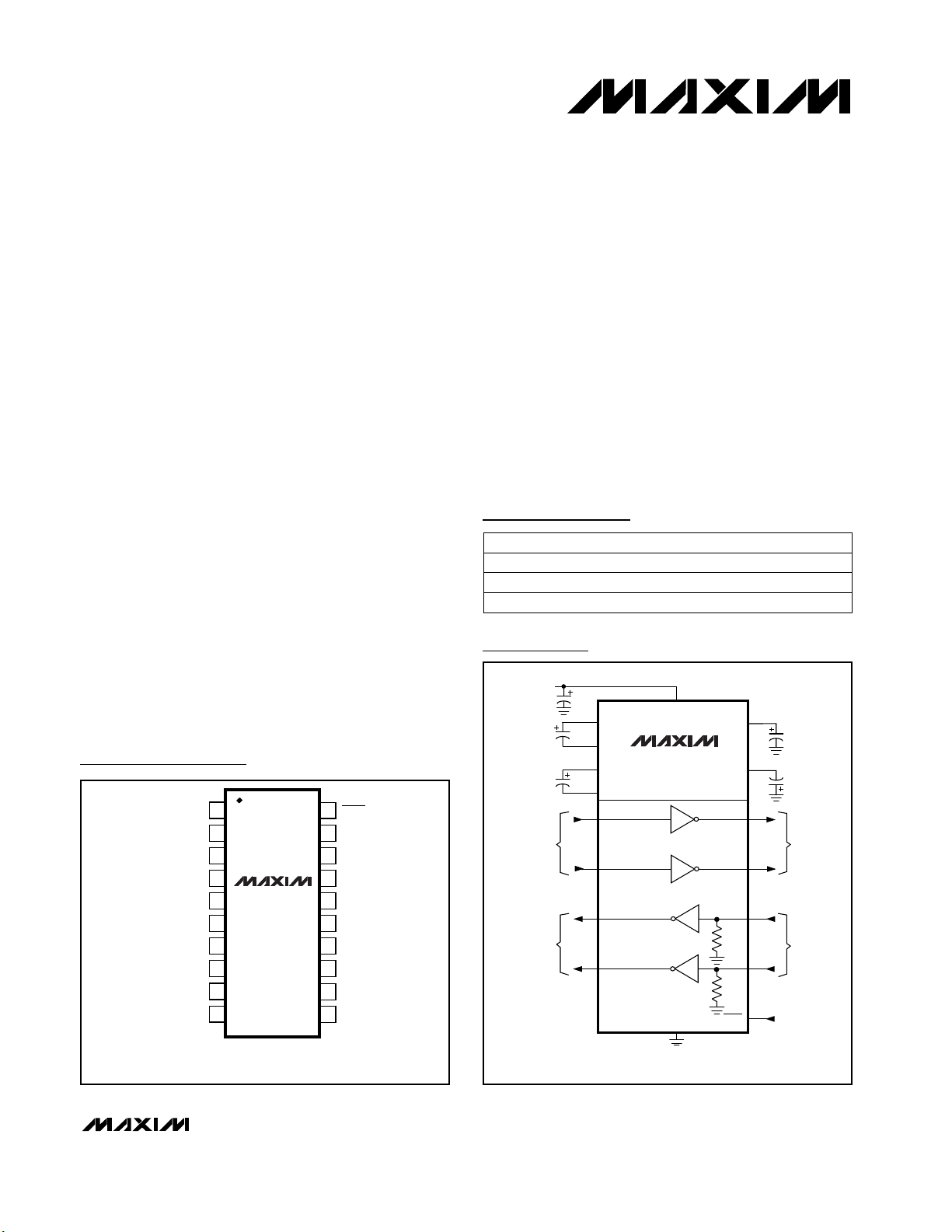
Pin Configurations
19-1949; Rev 0; 1/01
†
Covered by U.S. Patent numbers 4,636,930; 4,679,134; 4,777,577; 4,797,899; 4,809,152; 4,897,774; 4,999,761; and other patents pending.
Typical Operating Circuit
Ordering Information
PART
MAX3384ECAP
MAX3384EEAP -40°C to +85°C
0°C to +70°C
TEMP. RANGE PIN-PACKAGE
20 SSOP
20 SSOP
For price, delivery, and to place orders, please contact Maxim Distribution at 1-888-629-4642,
or visit Maxim’s website at www.maxim-ic.com.
MAX3384ECWN 0°C to +70°C 18 SO
Pin Configurations continued at end of data sheet.
TOP VIEW
N.C.
C1+
C1-
C2+
C2-
T2OUT
R2IN
N.C.
1
2
V+
3
4
MAX3384E
5
6
V-
7
8
9
10
SHDN
20
V
19
CC
GND
18
T1OUT
17
R1IN
16
R1OUT
15
T1IN
14
T2IN
13
R2OUT
12
N.C.
11
+3.3V
C
BYPASS
C1
0.1µF
C2
0.1µF
TTL/CMOS
INPUTS
TTL/CMOS
OUTPUTS
V
C1+
C1-
C2+
C2-
T1IN
T2IN
R1OUT
R2OUT
CC
MAX3384E
GND
T1OUT
T2OUT
R1IN
5k
R2IN
5k
SHDN
V+
V-
C3*
0.1µF
C4
0.1µF
RS-232
OUTPUTS
RS-232
INPUTS
SSOP
* C3 CAN BE RETURNED TO EITHER V
NOTE: SEE TABLE 2 FOR CAPACITOR SELECTION
OR GROUND.
CC
Page 2
MAX3384E
±15kV ESD-Protected, 3.0V to 5.5V, Low-Power,
up to 250kbps, True RS-232 Transceiver
2 _______________________________________________________________________________________
ABSOLUTE MAXIMUM RATINGS
ELECTRICAL CHARACTERISTICS
(VCC= +3V to +5.5V, for tests at 3.3V ±10%, C1–C4 = 0.1µF; for tests at +5V ±10%, C1 = 0.047µF, C2–C4 = 0.33µF;
T
A
= T
MIN
to T
MAX
, unless otherwise noted. Typical values are at TA= +25°C.)
Stresses beyond those listed under “Absolute Maximum Ratings” may cause permanent damage to the device. These are stress ratings only, and functional
operation of the device at these or any other conditions beyond those indicated in the operational sections of the specifications is not implied. Exposure to
absolute maximum rating conditions for extended periods may affect device reliability.
VCCto GND..............................................................-0.3V to +6V
V+ to GND (Note 1) ..................................................-0.3V to +7V
V- to GND (Note 1) ...................................................+0.3V to -7V
V+ + |V-| (Note 1) .................................................................+13V
Input Voltages
T_IN, SHDN to GND ..............................................-0.3V to +6V
R_IN to GND .....................................................................±25V
Output Voltages
T_OUT to GND...............................................................±13.2V
R_OUT.....................................................-0.3V to (V
CC
+ 0.3V)
Maximum Current into T_OUT ........................................±100mA
Short-Circuit Duration, T_OUT to GND.......................Continuous
Continuous Power Dissipation (T
A
= +70°C)
20-Pin SSOP (derate 8.00mW/°C above +70°C) ..........640mW
18-Pin SO (derate 9.52mW/°C above +70°C)...............762mW
Operating Temperature Ranges
MAX3384ECAP ....................................................0°C to +70°C
MAX3384ECWN...................................................0°C to +70°C
MAX3384EEAP .................................................-40°C to +85°C
Junction Temperature ........................................................150°C
Storage Temperature Range .............................-65°C to +150°C
Lead Temperature (soldering, 10s) .................................+300°C
TA = +25°C
SHDN = VCC, no load
TA = +25°C
TA = +25°C
I
OUT
= 1.6mA
R_OUT, receivers disabled
T_IN, SHDN
T_IN, SHDN
I
OUT
= -1.0mA
CONDITIONS
kΩ357Input Resistance
V0.5Input Hysteresis
V
1.8 2.4
Input Threshold High
1.5 2.4
V
0.8 1.5
Input Threshold Low
0.6 1.2
V-25 +25Input Voltage Range
V
VCC-VCC-
0.6 0.1
Output Voltage High
mA0.3 1Supply Current
V0.4Output Voltage Low
µA±0.05 ±10Output Leakage Current
V0.5Transmitter Input Hysteresis
V0.8Input Logic Threshold Low
2.0
V
2.4
Input Logic Threshold High
UNITSMIN TYP MAXPARAMETER
Note 1: V+ and V- can have maximum magnitudes of 7V, but their absolute difference cannot exceed 13V.
VCC= +5V
VCC= +3.3V
VCC= +3.3V
VCC= +5V
VCC= +3.3V
VCC= +5V
T_IN, SHDN
µA±0.01 ±1Input Leakage Current
SHDN = GND
µA110Shutdown Supply Current
DC CHARACTERISTICS (VCC= +3.3V or +5V, TA= +25°C)
LOGIC INPUTS
RECEIVER OUTPUTS
RECEIVER INPUTS
Page 3
MAX3384E
±15kV ESD-Protected, 3.0V to 5.5V, Low-Power,
up to 250kbps, True RS-232 Transceiver
_______________________________________________________________________________________ 3
Note 2: Transmitter skew is measured at the transmitter zero cross points.
ELECTRICAL CHARACTERISTICS (continued)
(VCC= +3V to +5.5V, for tests at 3.3V ±10%, C1–C4 = 0.1µF; for tests at +5V ±10%, C1 = 0.047µF, C2–C4 = 0.33µF;
T
A
= T
MIN
to T
MAX
, unless otherwise noted. Typical values are at TA= +25°C.)
Receiver input to receiver output,
CL= 150pF
RL= 3kΩ, CL= 1000pF,
one transmitter switching
VCC= +3.3V,
T
A
= +25°C,
RL= 3kΩ to 7kΩ,
measured from +3V
to -3V or -3V to +3V
V
OUT
≥ +3.7V, R
LOAD
at V+ = 3kΩ
(Note 2)
CONDITIONS
µs
0.15t
PLH
Receiver Propagation Delay
0.15t
PHL
kbps250Maximum Data Rate
630
µs250Time to Exit Shutdown
ns100
t
PHL
- t
PLH
|
Transmitter Skew
ns50
t
PHL
- t
PLH
|
Receiver Skew
UNITSMIN TYP MAXSYMBOLPARAMETER
VCC= 0, transmitter output = ±2V
All transmitter outputs loaded with 3kΩ to ground
IEC1000-4-2 Contact Discharge
IEC1000-4-2 Air Discharge
Human Body Model
VCC= 0 or +3V to +5.5V, V
OUT
= ±12V, transmitters dis-
CONDITIONS
Ω300 10MOutput Resistance
V±5 ±5.4Output Voltage Swing
±8
R_IN, T_OUT
±15
kV
±15
mA±60Output Short-Circuit Current
µA±25Output Leakage Current
UNITSMIN TYP MAXPARAMETER
TIMING CHARACTERISTICS
(VCC= +3V to +5.5V, for tests at 3.3V ±10%, C1–C4 = 0.1µF; for tests at +5V ±10%, C1 = 0.047µF, C2–C4 = 0.33µF; TA= T
MIN
to
T
MAX
, unless otherwise noted. Typical values are at TA= +25°C.)
CL= 150pF to
1000pF
CL= 150pF to
2500pF
V/µs
430
Transition-Region Slew Rate
TRANSMITTER OUTPUTS
ESD PROTECTION
SHDN from V
CC to
GND
ns200Receiver Output Disable Time
SHDN from GND to V
CC
ns200Receiver Output Enable Time
Page 4
MAX3384E
±15kV ESD-Protected, 3.0V to 5.5V, Low-Power,
up to 250kbps, True RS-232 Transceiver
4 _______________________________________________________________________________________
__________________________________________Typical Operating Characteristics
(VCC= +3.3V, 250kbps data rate, 0.1µF capacitors, all transmitters loaded with 3kΩ and CL, TA = +25°C, unless otherwise noted.)
-6
-5
-4
-3
-2
-1
0
1
2
3
4
5
6
0 1000 2000 3000 4000 5000
TRANSMITTER OUTPUT VOLTAGE
vs. LOAD CAPACITANCE
MAX3384E-01
LOAD CAPACITANCE (pF)
TRANSMITTER OUTPUT VOLTAGE (V)
T1 TRANSMITTING AT 250kbps
T2 TRANSMITTING AT 15.6kbps
V
OUT+
V
OUT-
0
6
2
4
10
8
14
12
16
0 1000 2000 3000 4000 5000
SLEW RATE vs. LOAD CAPACITANCE
MAX3884E-02
LOAD CAPACITANCE (pF)
SLEW RATE (V/µs)
+SLEW
FOR DATA RATES UP TO 250kbps
-SLEW
0
25
20
15
5
10
35
30
40
45
0 20001000 3000 4000 5000
OPERATING SUPPLY CURRENT
vs. LOAD CAPACITANCE
MAX3884E-03
LOAD CAPACITANCE (pF)
SUPPLY CURRENT (mA)
250kbps
120kbps
20kbps
T1 TRANSMITTING AT 250kbps
T2 TRANSMITTING AT 15.6kbps
1 No Connection. Not internally connected.N.C.
3 +5.5V generated by the charge pump.V+
4 Negative terminal of the voltage-doubler charge-pump capacitor.C1-
5 Positive terminal of inverting charge-pump capacitor.C2+
6 Negative terminal of inverting charge-pump capacitor.C2-
7 -5.5V generated by the charge pump.V-
8, 15
RS-232 Transmitter Outputs. High Z when SHDN is low.
T_OUT
9, 14 RS-232 Receiver InputsR_IN
10, 13
TTL/CMOS Receiver Outputs. High Z when SHDN is low.
R_OUT
11, 12 TTL/CMOS Transmitter InputsT_IN
16 GroundGND
17 +3.0V to +5.5V Supply Voltage. Connect a 0.1µF capacitor to GND.V
CC
18
Active-Low Shutdown-Control Input. Drive low to shut down transmitters, receivers and
charge pumps.
SHDN
FUNCTIONNAME
______________________________________________________________ Pin Description
2 Positive terminal of the voltage-doubler charge-pump capacitor.C1+
PIN
2
1, 10, 11
3
4
5
6
7
8, 17
9, 16
12, 15
13, 14
18
19
20
SO SSOP
Page 5

MAX3384E
±15kV ESD-Protected, 3.0V to 5.5V, Low-Power,
up to 250kbps, True RS-232 Transceiver
_______________________________________________________________________________________ 5
_______________Detailed Description
Dual Charge-Pump Voltage Converter
The MAX3384E’s internal power supply consists of a
regulated dual charge pump that provides output voltages of +5.5V (doubling charge pump) and -5.5V
(inverting charge pump), over the +3.0V to +5.5V V
CC
range. The charge pump operates in discontinuous
mode; if the output voltages are less than 5.5V, the
charge pump is enabled, and if the output voltages
exceed 5.5V, the charge pump is disabled. Each
charge pump requires a flying capacitor (C1, C2) and a
reservoir capacitor (C3, C4) to generate the V+ and Vsupplies (Figure 1).
RS-232 Transmitters
The transmitters are inverting level translators that convert CMOS-logic levels to ±5.0V EIA/TIA-232 levels.
The MAX3384E transmitters guarantee a 250kbps data
rate with worst-case loads of 3kΩ in parallel with 1000pF,
providing compatibility with PC-to-PC communication
software (such as LapLink™). Transmitters can be paralleled to drive multiple receivers or mice.
The MAX3384E’s transmitters are disabled and the outputs are forced into a high-impedance state when the
device is in shutdown (SHDN = GND). The MAX3384E
permits the outputs to be driven up to ±12V in shutdown.
The transmitter inputs do not have pullup resistors.
Connect unused inputs to GND or V
CC
.
RS-232 Receivers
The receivers convert RS-232 signals to CMOS-logic
output levels (Table 1). The receiver outputs are forced
into a high-impedance state when the device is in shutdown (SHDN = GND). This allows a single UART to
multiplex between different protocols.
Shutdown Mode
Supply current falls to less than 1µA in shutdown mode
(SHDN = low). When shut down, the device’s charge
0
SHDN
1
High-Z
T_OUT
Active
High-Z
R_OUT
Active
Figure 1. Slew-Rate Test Circuits
Table 1. Shutdown Truth Table
Laplink is a trademark of Traveling Software.
V
CC
0.1µF
V
CC
0.1µF
V
C1+
C1
C2
V
CC
C1-
C2+
C2-
T_ IN
R_ OUT
SHDN
MINIMUM SLEW-RATE TEST CIRCUIT MAXIMUM SLEW-RATE TEST CIRCUIT
CC
MAX3384E
GND
5kΩ
V+
V-
T_ OUT
R_ IN
3kΩ
3kΩ
C3
C4
2500pF
V
CC
MAX3384E
GND
5kΩ
T_ OUT
R_ IN
V+
3kΩ
C3
V-
C4
7kΩ
150pF
C1
C2
C1+
C1-
C2+
C2-
T_ IN
R_ OUT
V
CC
SHDN
Page 6

pumps are shut off, V+ is pulled down to VCC, V- is
pulled to ground, and the transmitter and receiver outputs are disabled (high impedance). The time required
to exit shutdown is typically 100µs, as shown in Figure
2. Connect SHDN to VCCif the shutdown mode is not
used.
±15kV ESD Protection
As with all Maxim devices, ESD-protection structures
are incorporated on all pins to protect against electrostatic discharges encountered during handling and
assembly. The driver outputs and receiver inputs of the
MAX3384E have extra protection against static electricity. Maxim’s engineers have developed state-of-the-art
structures to protect these pins against ESD of ±15kV
without damage. The ESD structures withstand high
ESD in all states: normal operation, shutdown, and
powered down. After an ESD event, Maxim’s “E” versions keep working without latchup, whereas competing RS-232 products can latch and must be powered
down to remove latchup.
ESD protection can be tested in various ways; the
transmitter outputs and receiver inputs of this product
family are characterized for protection to the following
limits:
1) ±15kV using the Human Body Model
2) ±8kV using the contact-discharge method specified
in IEC 1000-4-2
3) ±15kV using IEC 1000-4-2’s air-gap method.
ESD Test Conditions
ESD performance depends on a variety of conditions.
Contact Maxim for a reliability report that documents
test setup, test methodology, and test results.
Human Body Model
Figure 3a shows the Human Body Model, and Figure
3b shows the current waveform it generates when discharged into a low impedance. This model consists of a
100pF capacitor charged to the ESD voltage of interest,
which is then discharged into the test device through a
1.5kΩ resistor.
IEC 1000-4-2
The IEC 1000-4-2 standard covers ESD testing and performance of finished equipment; it does not specifically
refer to integrated circuits. The MAX3384E helps you
design equipment that meets Level 4 (the highest level) of
IEC 1000-4-2, without the need for additional ESD-protection components.
The major difference between tests done using the
Human Body Model and IEC 1000-4-2 is higher peak
current in IEC 1000-4-2, because series resistance is
lower in the IEC 1000-4-2 model. Hence, the ESD withstand voltage measured to IEC 1000-4-2 is generally
lower than that measured using the Human Body
Model. Figure 4a shows the IEC 1000-4-2 model, and
Figure 4b shows the current waveform for the ±8kV IEC
1000-4-2 Level 4 ESD contact-discharge test.
The air-gap test involves approaching the device with a
charged probe. The contact-discharge method connects the probe to the device before the probe is energized.
Machine Model
The Machine Model for ESD tests all pins using a
200pF storage capacitor and zero discharge resistance. Its objective is to emulate the stress caused by
contact that occurs with handling and assembly during
manufacturing. Of course, all pins require this protection during manufacturing, not just RS-232 inputs and
outputs. Therefore, after PC board assembly, the
Machine Model is less relevant to I/O ports.
Applications Information
Capacitor Selection
The capacitor type used for C1–C4 is not critical for
proper operation; polarized or nonpolarized capacitors
MAX3384E
±15kV ESD-Protected, 3.0V to 5.5V, Low-Power,
up to 250kbps, True RS-232 Transceiver
Figure 2. Transmitter Outputs Exiting Shutdown or
Powering Up
0.1
0.047
C1, C
BYPASS
(µF)
0.1
0.1
0.33
C2, C3, C4
(µF)
0.47
3.0 to 3.6
4.5 to 5.5
V
CC
(V)
3.0 to 5.5
Table 2. Required Minimum Capacitance
Values
6 _______________________________________________________________________________________
5V/div
0
2V/div
0
VCC = 3.3V
C1–C4 = 0.1µF
40µs/div
SHDN
T2OUT
T1OUT
Page 7

can be used. The charge pump requires 0.1µF capacitors for 3.3V operation. For other supply voltages, refer
to Table 2 for required capacitor values. Do not use values smaller than those listed in Table 2. Increasing the
capacitor values (e.g., by a factor of 2) reduces ripple
on the transmitter outputs and slightly reduces power
consumption. C2, C3, and C4 can be increased without
changing C1’s value. However, do not increase C1
without also increasing the values of C2, C3, C4,
and C
BYPASS
to maintain the proper ratios (C1 to
the other capacitors).
When using the minimum required capacitor values,
make sure the capacitor value does not degrade
excessively with temperature. If in doubt, use capacitors with a larger nominal value. The capacitor’s equiva-
lent series resistance (ESR), which usually rises at low
temperatures, influences the amount of ripple on V+
and V-.
Power-Supply Decoupling
In most circumstances, a 0.1µF VCCbypass capacitor
is adequate. In applications that are sensitive to powersupply noise, use a capacitor of the same value as
charge-pump capacitor C1. Connect bypass capacitors as close to the IC as possible.
Operation Down to 2.7V
Transmitter outputs will meet EIA/TIA-562 levels of
±3.7V with supply voltages as low as 2.7V.
MAX3384E
±15kV ESD-Protected, 3.0V to 5.5V, Low-Power,
up to 250kbps, True RS-232 Transceiver
_______________________________________________________________________________________ 7
Figure 3a. Human Body ESD Test Model
Figure 3b. Human Body Model Current Waveform
Figure 4a. IEC 1000-4-2 ESD Test Model
Figure 4b. IEC 1000-4-2 ESD Generator Current Waveform
HIGH-
VOLTAGE
DC
SOURCE
R
C
1M
CHARGE-CURRENT
LIMIT RESISTOR
C
100pF
s
R
D
1500Ω
DISCHARGE
RESISTANCE
STORAGE
CAPACITOR
HIGH-
VOLTAGE
DC
SOURCE
R
C
50M to 100M
CHARGE-CURRENT
LIMIT RESISTOR
C
150pF
s
RD
330Ω
DISCHARGE
RESISTANCE
STORAGE
CAPACITOR
DEVICE
UNDER
TEST
DEVICE
UNDER
TEST
PEAK-TO-PEAK RINGING
I
r
(NOT DRAWN TO SCALE)
AMPERES
IP 100%
90%
36.8%
10%
0
0
t
RL
TIME
t
DL
CURRENT WAVEFORM
I
100%
90%
PEAK
I
10%
tr = 0.7ns to 1ns
30ns
60ns
t
Page 8

Figure 6. Loopback Test Circuit
Figure 7. MAX3384E Loopback Test Result at 120kbps
Figure 8. MAX3384E Loopback Test Result at 250kbps
MAX3384E
±15kV ESD-Protected, 3.0V to 5.5V, Low-Power,
up to 250kbps, True RS-232 Transceiver
8 _______________________________________________________________________________________
Transmitter Outputs when
Exiting Shutdown
Figure 2 shows two transmitter outputs when exiting
shutdown mode. As they become active, the two transmitter outputs are shown going to opposite RS-232 levels (one transmitter input is high, the other is low). Each
transmitter is loaded with 3kΩ in parallel with 2500pF.
The transmitter outputs display no ringing or undesirable transients as they come out of shutdown. Note that
the transmitters are enabled only when the magnitude
of V- exceeds approximately -3V.
High Data Rates
The MAX3384E maintains the RS-232 ±5.0V minimum
transmitter output voltage even at high data rates.
Figure 6 shows a transmitter loopback test circuit.
Figure 7 shows a loopback test result at 120kbps, and
Figure 8 shows the same test at 250kbps. For Figure 7,
all transmitters were driven simultaneously at 120kbps
into RS-232 loads in parallel with 1000pF. For Figure 8,
a single transmitter was driven at 250kbps, and all
transmitters were loaded with an RS-232 receiver in
parallel with 1000pF.
V
CC
0.1µF
V
CC
MAX3384E
V+
V-
T_ OUT
C1
C2
C1+
C1-
C2+
C2-
T_ IN
T1IN
C3
T1OUT
C4
R1OUT
VCC = 3.3V
C1–C4 = 0.1µF
2µs/div
5V/div
5V/div
5V/div
5kΩ
R_ IN
1000pF
T1IN
T1OUT
R1OUT
VCC = 3.3V
C1–C4 = 0.1µF
2µs/div
R_ OUT
V
CC
SHDN
GND
5V/div
5V/div
5V/div
Page 9

Interconnection with 3V and 5V Logic
The MAX3384E can directly interface with various 5V
logic families, including ACT and HCT CMOS. See
Table 3 for more information on possible combinations
of interconnections.
MAX3384E
±15kV ESD-Protected, 3.0V to 5.5V, Low-Power,
up to 250kbps, True RS-232 Transceiver
_______________________________________________________________________________________ 9
Table 3. Logic-Family Compatibility with
Various Supply Voltages
5
SYSTEM
POWER-SUPPLY
VOLTAGE
(V)
5
3.3
Compatible with ACT
and HCT CMOS, and
with AC, HC, or
CD4000 CMOS
COMPATIBILITY
Compatible with all TTL
and CMOS families
Compatible with all
CMOS families
3.3
VCCSUPPLY
VOLTAGE
(V)
5
3.3
18
17
16
15
14
13
1
2
3
8
12
11
10
4
5
6
7
SHDN
V
CC
GND
T1OUT
C1-
V+
C1+
N.C.
R1IN
R1OUT
T2IN
R2OUT
T2OUT
V-
C2-
C2+
9
R2IN
SO
T1IN
MAX3384E
TOP VIEW
Pin Configurations (continued)
___________________Chip Information
TRANSISTOR COUNT: 1129
Process: BiCMOS
Page 10

MAX3384E
±15kV ESD-Protected, 3.0V to 5.5V, Low-Power,
up to 250kbps, True RS-232 Transceiver
10 ______________________________________________________________________________________
________________________________________________________Package Information
SSOP.EPS
Page 11

MAX3384E
±15kV ESD-Protected, 3.0V to 5.5V, Low-Power,
up to 250kbps, True RS-232 Transceiver
Package Information (continued)
Maxim cannot assume responsibility for use of any circuitry other than circuitry entirely embodied in a Maxim product. No circuit patent licenses are
implied. Maxim reserves the right to change the circuitry and specifications without notice at any time.
11 ____________________Maxim Integrated Products, 120 San Gabriel Drive, Sunnyvale, CA 94086 408-737-7600
© 2001 Maxim Integrated Products Printed USA is a registered trademark of Maxim Integrated Products.
SOICW.EPS
 Loading...