

Page 1
General Description
The MAX3349EA ±15kV ESD-protected, USB transceiver provides a full-speed USB interface to a lower voltage
microprocessor or ASIC. The device supports enumeration, suspend, and VBUS detection. A special UART
multiplexing mode routes external UART signals (Rx and
Tx) to D+ and D-, allowing the use of a shared connector to reduce cost and part count for mobile devices.
The UART interface allows mobile devices such as
PDAs, cellular phones, and digital cameras to use either
UART or USB signaling through the same connector.
The MAX3349EA features a separate UART voltage supply input to support legacy devices using +2.75V signaling. The MAX3349EA supports a maximum UART baud
rate of 921kbaud.
Upon connection to a USB host, the MAX3349EA enters
USB mode and provides a full-speed USB 2.0 compliant
interface through VP, VM, RCV, and OE. The
MAX3349EA features internal series termination resistors
on D+ and D-, and an internal 1.5kΩ pullup resistor to
D+ to allow the device to logically connect and disconnect from the USB while plugged in. A suspend mode is
provided for low-power operation. D+ and D- are protected from electrostatic discharge (ESD) up to ±15kV.
The MAX3349EA is available in 16-pin TQFN (4mm x
4mm) and 16-bump UCSP™ (2mm x 2mm) packages,
and is specified over the -40°C to +85°C extended temperature range.
Applications
Cell Phones
PDAs
Digital Cameras
MP3 Players
Features
♦ ±15kV ESD HBM Protection on D+ and D-
♦ UART Mode Routes External UART Signals to
D+/D-
♦ Internal Linear Regulator Allows Direct Powering
from the USB Cable
♦ Separate Voltage Input for UART
Transmitter/Receiver (V
UART
)
♦ Internal 1.5kΩ Pullup Resistor on D+ Controlled
by Enumerate Input
♦ Internal Series Termination Resistors on D+ and D-
♦ Complies with USB Specification Revision 2.0,
Full-Speed 12Mbps Operation
♦ Built-In Level Shifting Down to +1.4V, Ensuring
Compatibility with Low-Voltage ASICs
♦ V
BUS
Detection
♦ Combined VP and VM Inputs/Outputs
♦ No Power-Supply Sequencing Required
♦ Available in 16-Bump UCSP (2mm x 2mm)
Package
MAX3349EA
USB 2.0 Full-Speed Transceiver with UART
Multiplexing Mode
________________________________________________________________ Maxim Integrated Products 1
19-0667; Rev 0; 10/06
For pricing, delivery, and ordering information, please contact Maxim/Dallas Direct! at
1-888-629-4642, or visit Maxim’s website at www.maxim-ic.com.
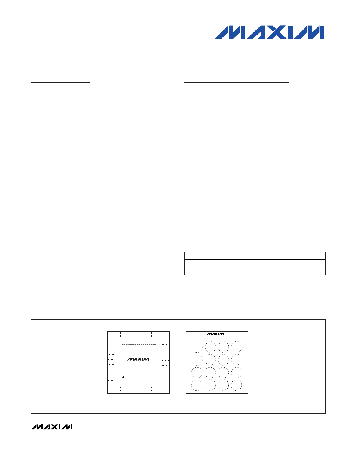
Ordering Information
TQFN-EP (4mm x 4mm)
ENUM
16
1234
12 11 10 9
15
14
13
5
6
7
8
VM
V
L
V
TRM
V
BUS
D+
D-
GND
RX
TX
BD
VP
RCV
OE
SUS
V
UART
MAX3349EA
TOP VIEW
*EP
+
UCSP (2mm x 2mm)
(BUMPS ON BOTTOM OF DIE)
MAX3349EA
TOP VIEW
A
B
C
1
23
RX
TX
V
UART
VP
V
L
ENUM
SUS
V
TRM
BD
VM
RCV
OE
4
D
D+
D-
V
BUS
GND
*EXPOSED PADDLE—CONNECT TO GND OR LEAVE UNCONNECTED.
+
+ DENOTES LEAD-FREE PACKAGE.
Pin Configurations
UCSP is a trademark of Maxim Integrated Products, Inc.
Note: All devices specified for the -40°C to +85°C extended
temperature range.
**Future product—contact factory for availability.
*EP = Exposed paddle.
+Indicates lead-free package.
PART PIN-PACKAGE PKG CODE
MAX3349EAEBE+T 16 UCSP B16-1
MAX3349EAETE** 16 TQFN-EP* T1644-4
Page 2
MAX3349EA
USB 2.0 Full-Speed Transceiver with UART
Multiplexing Mode
2 _______________________________________________________________________________________
ABSOLUTE MAXIMUM RATINGS
Stresses beyond those listed under “Absolute Maximum Ratings” may cause permanent damage to the device. These are stress ratings only, and functional
operation of the device at these or any other conditions beyond those indicated in the operational sections of the specifications is not implied. Exposure to
absolute maximum rating conditions for extended periods may affect device reliability.
(All voltages referenced to GND, unless otherwise noted.)
V
UART
, VL, V
BUS
, D+, D- ..........................................-0.3V to +6V
V
TRM
.........................................................-0.3V to (V
BUS
+ 0.3V)
VP, VM, SUS, RX, TX, ENUM, RCV, OE, BD, -0.3V to (V
L
+ 0.3V)
Short Circuit Current (D+ and D-)...................................±150mA
Maximum Continuous Current (all other pins) .................±15mA
Continuous Power Dissipation (T
A
= +70°C)
16-Bump UCSP (derate 8.2mW/°C above +70°C) ....659.5mW
16-Pin 4mm x 4mm TQFN (derate 25.0mW/°C
above +70°C).............................................................2000mW
Operating Temperature Range ...........................-40°C to +85°C
Junction Temperature .....................................................+150°C
Storage Temperature Range .............................-65°C to +150°C
Lead Temperature (soldering, 10s) .................................+300°C
Bump Temperature (soldering, reflow) ............................+235°C
ELECTRICAL CHARACTERISTICS
(V
BUS
= +4.0V to +5.5V, V
UART
= +2.7V to +3.3V, VL= +1.40V to +2.75V, TA= -40°C to +85°C, unless otherwise noted. Typical val-
ues are at V
BUS
= +5V, VL= +1.8V, V
UART
= +2.75V (UART Mode), and TA= +25°C.) (Note 1)
PARAMETER SYMBOL CONDITIONS
MIN
TYP
MAX
UNITS
SUPPLY INPUTS/OUTPUTS (V
BUS
, V
UART
, V
TRM
, VL)
V
BUS
Input Range V
BUS
USB mode 4.0 5.5 V
VL Input Range V
L
V
V
UART
Input Range V
UART
UART mode 2.7 3.3 V
Regulated Supply-Voltage Output
V
TRM
Internal regulator, USB mode 3.0 3.6 V
Operating V
BUS
Supply Current I
BUS
Full-speed transmitting/receiving at
12Mbps, C
L
= 50pF on D+ and D-
10 mA
Operating V
UART
Supply Current
I
VUART
UART transmitting/receiving at
921kbaud, C
L
= 200pF
2.5 mA
Static V
UART
Supply Current
)
UART mode 3.5 5 µA
Operating VL Supply Current I
VL
Full-speed transmitting/receiving at
12Mbps, C
L
= 50pF on D+ and D-
6mA
Full-speed idle,
V
D+
> +2.7V, V
D-
< +0.3V
400
Full-Speed Idle and SE0 Supply
Current
I
VBUS(IDLE)
SE0: VD+ < +0.3V, VD- < +0.3V
450
µA
Static VL Supply Current I
VL(STATIC)
Full-speed idle, SE0, suspend mode, or
static UART mode
210µA
Sharing Mode VL Supply Current
I
VL(OFF)
V
BUS
and V
UART
not present 2 5 µA
USB Suspend V
BUS
Supply
Current
I
VBUS(SUS)
VM, VP unconnected;
OE = 1, SUS = 1
38 65 µA
V
BUS
DETECTION (BD)
VL = +1.8V 1.8 2.7 3.4
USB Power-Supply Detection
Threshold
V
TH_VBUS
VL = +2.5V 2.3 3.2 4.0
V
VL = +1.8V 80
USB Power-Supply Detection
Hysteresis
V
HYS_VBUS
VL = +2.5V
mV
VL Power-Supply Detection
Threshold
V
TH_VL
0.7 V
1.40 2.75
I
VUART(STATIC
290
340
100
Page 3
MAX3349EA
USB 2.0 Full-Speed Transceiver with UART
Multiplexing Mode
_______________________________________________________________________________________ 3
ELECTRICAL CHARACTERISTICS (continued)
(V
BUS
= +4.0V to +5.5V, V
UART
= +2.7V to +3.3V, VL= +1.40V to +2.75V, TA= -40°C to +85°C, unless otherwise noted. Typical val-
ues are at V
BUS
= +5V, VL= +1.8V, V
UART
= +2.75V (UART Mode), and TA= +25°C.) (Note 1)
PARAMETER SYMBOL CONDITIONS
UNITS
V
UART
Power-Supply Detection
Threshold
V
TH_UART
0.4 x
V
L
0.65 x
V
L
0.9 x
V
L
V
DIGITAL INPUTS/OUTPUTS (VP, VM, RCV, SUS, OE, RX, TX, ENUM, BD)
Input Voltage Low V
IL
0.3 x
V
L
V
Input Voltage High V
IH
0.7 x
V
L
V
Output Voltage Low V
OL
IOL = +2mA, VL > 1.65V
I
OL
= +1mA, VL < 1.65V
0.4 V
Output Voltage High V
OH
IOH = +2mA, VL > 1.65V
I
OH
= +1mA, VL < 1.65V
V
L
V
Input Leakage Current I
LKG
-1 +1 µA
ANALOG INPUTS/OUTPUTS (D+, D- in USB Mode)
Differential Input Sensitivity V
ID
|VD+ - VD-| 0.2 V
Differential Common-Mode
Voltage
V
CM
Includes V
ID
range 0.8 2.5 V
Single-Ended Input
Low Voltage
V
ILSE
0.8 V
Single-Ended Input
High Voltage
V
IHSE
2.0 V
USB Output Voltage Low V
USB_OLD
RL = 1.5kΩ connected to +3.6V 0.3 V
USB Output Voltage High V
USB_OHD
RL = 15kΩ connected to GND 2.8 3.6 V
Off-State Leakage Current I
LZ
-10
µA
Driver Output Impedance Z
DRV
Steady-state drive
38
Ω
Transceiver Capacitance C
IND
Measured from D+/D- to GND 20 pF
Input Impedance Z
IN
Driver off 0.9 1.3 2.0 MΩ
D+ Internal Pullup Resistor R
PU
ENUM = 1
Ω
ANALOG INPUTS/OUTPUTS (D+, D- in UART Mode)
Input Voltage High V
UART_IH
2.0 V
Input Voltage Low V
UART_IL
UART mode,
+2.70V < V
UART
< +2.85V
0.8 V
Output Voltage High V
UART_OH
UART mode,
+2.70V < V
UART
< +2.85V
I
UART_OH
= -2mA
2.2 V
Output Voltage Low V
UART_OL
UART mode,
+2.70V < V
UART
< +2.85V
I
UART_OL
= +2mA
0.4 V
UART mode, +2.70 < V
MIN TYP MAX
0.4
29.0
1425 1500 1575
< +2.85V
UART
+10
43.5
Page 4
MAX3349EA
USB 2.0 Full-Speed Transceiver with UART
Multiplexing Mode
4 _______________________________________________________________________________________
ELECTRICAL CHARACTERISTICS (continued)
(V
BUS
= +4.0V to +5.5V, V
UART
= +2.7V to +3.3V, VL= +1.40V to +2.75V, TA= -40°C to +85°C, unless otherwise noted. Typical val-
ues are at V
BUS
= +5V, VL= +1.8V, V
UART
= +2.75V (UART Mode), and TA= +25°C.) (Note 1)
PARAMETER SYMBOL CONDITIONS
MIN
TYP
MAX
UNITS
ESD PROTECTION (D+, D-)
Human Body Model (Figures 9 and 10)
kV
IEC 61000-4-2
Air-Gap Discharge
±8 kV
IEC 61000-4-2
Contact Discharge
±8 kV
TIMING CHARACTERISTICS
(V
BUS
= +4.0V to +5.5V, V
UART
= +2.7V to +3.3V, VL= +1.4V to +2.75V, TA= -40°C to +85°C, unless otherwise noted. Typical values
are at V
BUS
= +5V, VL= +1.8V, V
UART
= +2.75V (UART Mode), and TA= +25°C.) (Note 1)
PARAMETER SYMBOL CONDITIONS
UNITS
USB DRIVER CHARACTERISTICS (CL = 50pF)
Rise Time t
FR
10% to 90% of | V
USB_OHD
- V
USB_OLD
|
(Figures 1 and 7)
420ns
Fall Time t
FF
90% to 10% of | V
USB_OHD
- V
USB_OLD
|
(Figures 1 and 7)
420ns
Rise/Fall Time Matching tFR/t
FF
Excluding the first transition from idle
state (Note 2) (Figures 1 and 7)
90
%
Output Signal Crossover Voltage
V
CRS_F
Excluding the first transition from idle
state (Note 2) (Figure 2)
1.3 2.0 V
VL > +1.65V (Figures 2 and 7)
t
PLH_DRV
+1.4V < VL < +1.65V (Figures 2 and 7) 25
VL > +1.65V (Figures 2 and 7)
Driver Propagation Delay
t
PHL_DRV
+1.4V < VL < +1.65V (Figures 2 and 7) 25
ns
t
PHZ_DRV
High-to-off transition (Figures 3 and 6) 25
Driver Disable Delay
t
PLZ_DRV
Low-to-off transition (Figures 3 and 6) 25
ns
t
PZH_DRV
Off-to-high transition (Figures 3 and 7) 25
Driver Enable Delay
t
PZL_DRV
Off-to-low transition (Figures 3 and 7) 25
ns
USB RECEIVER CHARACTERISTICS (CL = 15pF)
VL > +1.65V (Figures 4 and 8) 25
t
PLH_RCV
+1.4V < VL < +1.65V (Figures 4 and 8) 30
VL > +1.65V (Figures 4 and 8) 25
Differential Receiver Propagation
Delay
t
PHL_RCV
1.4V < VL < +1.65V (Figures 4 and 8) 30
ns
VL > +1.65V (Figures 4 and 8) 28
t
PLH_SE
+1.4V < VL < +1.65V (Figures 4 and 8) 35
VL > +1.65V (Figures 4 and 8) 28
Single-Ended Receiver
Propagation Delay
t
PHL_SE
+1.4V < VL < +1.65V (Figures 4 and 8) 35
ns
MIN TYP MAX
±15
110
22.5
22.5
Page 5
MAX3349EA
USB 2.0 Full-Speed Transceiver with UART
Multiplexing Mode
_______________________________________________________________________________________ 5
TIMING CHARACTERISTICS (continued)
(V
BUS
= +4.0V to +5.5V, V
UART
= +2.7V to +3.3V, VL= +1.4V to +2.75V, TA= -40°C to +85°C, unless otherwise noted. Typical values
are at V
BUS
= +5V, VL= +1.8V, V
UART
= +2.75V (UART Mode), and TA= +25°C.) (Note 1)
PARAMETER SYMBOL CONDITIONS
MIN
TYP
MAX
UNITS
High-to-off transition,
V
L
> +1.65V (Figure 5)
10
t
PHZ_SE
High-to-off transition,
+1.4V < V
L
< +1.65V (Figure 5)
12
Low-to-off transition,
V
L
> +1.65V (Figure 5)
10
Single-Ended Receiver Disable
Delay
t
PLZ_SE
Low-to-off transition,
+1.4V < V
L
< +1.65V (Figure 5)
12
ns
Off-to-high transition,
V
L
> +1.65V (Figure 5)
20
t
PZH_SE
Off-to-high transition,
+1.4V < V
L
< +1.65 (Figure 5)
20
Off-to-low transition,
V
L
> +1.65V (Figure 5)
20
Single-Ended Receiver Enable
Delay
t
PZL_SE
Off-to-low transition,
+1.4V < V
L
< +1.65V (Figure 5)
20
ns
UART DRIVER CHARACTERISTICS (CL = 200pF)
Rise Time (D-) t
FR_TUART
60
ns
Fall Time (D-) t
FF_TUART
60
ns
(Figure 13) 70
Driver Propagation Delay
(Figure 13) 70
ns
UART RECEIVER CHARACTERISTICS (CL = 15pF)
(Figure 14) 60
Receiver (Rx) Propagation Delay
(Figure 14) 60
ns
t
FR_RUART
(Figure 14) 45
Receiver (Rx) Rise/Fall Time
t
FF_RUART
(Figure 14) 45
ns
Note 1: Parameters are 100% production tested at TA=+25°C, unless otherwise noted. Limits over temperature are guaranteed
by design.
Note 2: Guaranteed by design, not production tested.
10% to 90% of |V
90% to 10% of |V
t
PLH_TUART
t
PHL_TUART
t
PLH_RUART
t
PHL_RUART
OHD
OHD
- V
- V
| (Figure 13)
OLD
| (Figure 13)
OLD
200
200
200
200
Page 6
MAX3349EA
USB 2.0 Full-Speed Transceiver with UART
Multiplexing Mode
6 _______________________________________________________________________________________
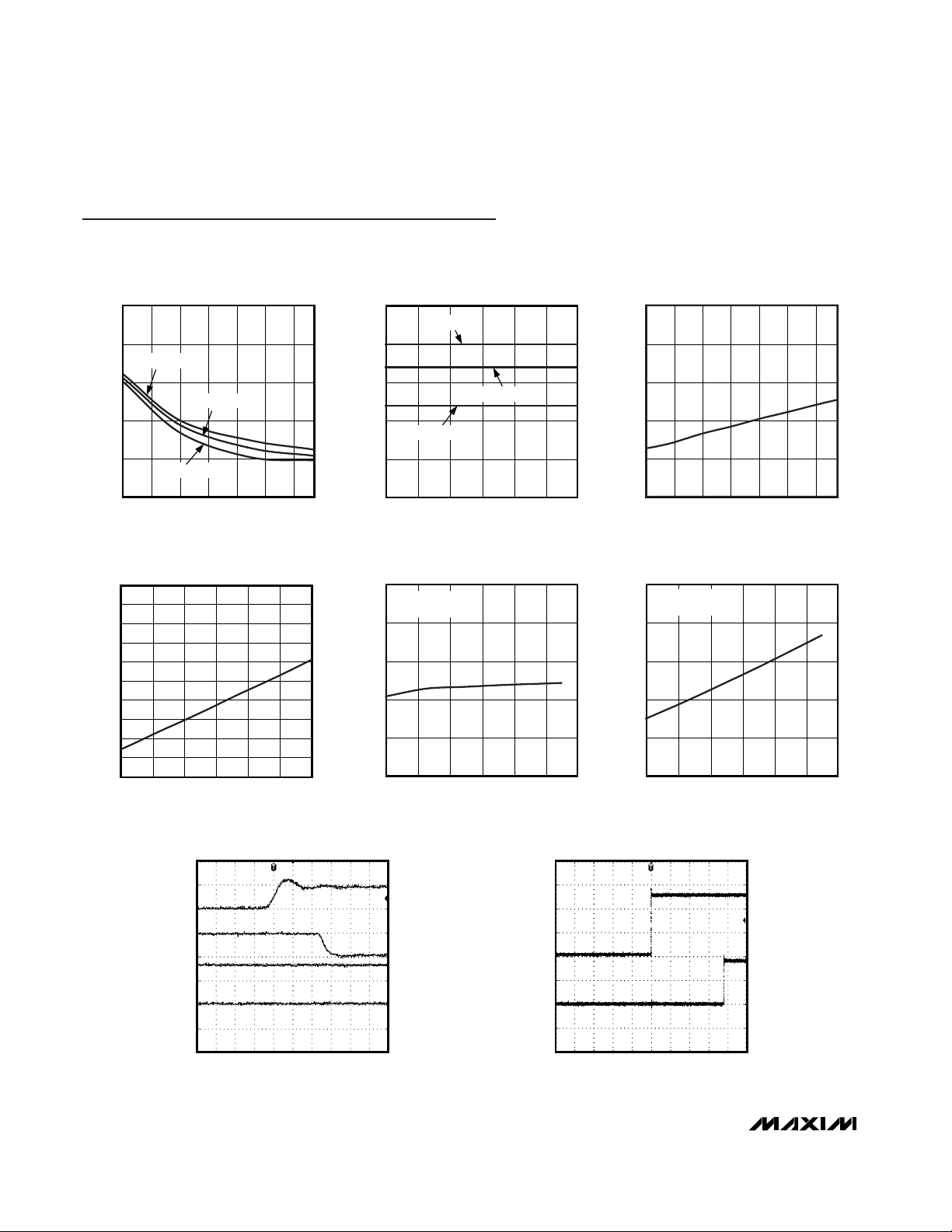
Typical Operating Characteristics
(V
BUS
= +5V, VL= +3.3V, V
UART
= +2.75V, TA= +25°C, unless otherwise noted.)
0
10
30
20
40
50
1.4 1.81.6 2.0 2.2 2.4 2.6
SINGLE-ENDED RECEIVER
PROPAGATION DELAY vs. V
L
MAX3349EA toc01
VL (V)
PROPAGATION DELAY (ns)
TA = +85°C
TA = +25°C
TA = -40°C
12
14
18
16
20
22
4.00 4.504.25 4.75 5.00 5.25 5.50
SINGLE-ENDED RECEIVER
PROPAGATION DELAY vs. V
BUS
MAX3349EA toc02
V
BUS
(V)
PROPAGATION DELAY (ns)
TA = +85°C
TA = +25°C
TA = -40°C
0
1
3
2
4
5
1.4 1.81.6 2.0 2.2 2.4 2.6
LOGIC CURRENT CONSUMPTION
IN SUSPEND MODE
MAX3349EA toc03
VL (V)
I
VL
(µA)
30
33
32
31
34
35
36
37
38
39
40
4.00 4.504.25 4.75 5.00 5.25 5.50
V
BUS
CURRENT CONSUMPTION
IN SUSPEND MODE
MAX3349EA toc04
V
BUS
(V)
I
VCC
(µA)
0.45
0.47
0.51
0.49
0.53
0.55
08040 120 160 200 240
VL CURRENT DURING USB OPERATION
vs. D+/D- CAPACITANCE
MAX3349EA toc05
D+/D- CAPACITANCE (CL)
I
VL
(mA)
12Mbps DATA RATE
TRANSMITTING
0
4
12
8
16
20
08040 120 160 200 240
V
BUS
CURRENT DURING USB OPERATION
vs. D+/D- CAPACITANCE
MAX3349EA toc06
D+/D- CAPACITANCE (CL)
I
VBUS
(mA)
12Mbps DATA RATE
TRANSMITTING
10ns/div
SUSPEND MODE
RCV
2V/div
SUS
2V/div
MAX3349EA toc07
4µs/div
BUS DETECT RESPONSE
BD
1V/div
V
BUS
2V/div
MAX3349EA toc08
Page 7

MAX3349EA
USB 2.0 Full-Speed Transceiver with UART
Multiplexing Mode
_______________________________________________________________________________________ 7
Pin Description
PIN
UCSP
TYPE NAME FUNCTION
A1 1
V
UART
UART Supply Voltage. V
UART
powers the internal UART transmitter and receiver.
Connect a regulated voltage between +2.7V and +3.3V to V
UART
. Bypass V
UART
to
GND with a 0.1µF ceramic capacitor.
A2 2
RX
UART Receive Output. In UART mode, RX is a level-shifted output that expresses
the logic state of D+.
A3 3 INPUT TX UART Transmit Input. In UART mode, D- follows the logic state on TX.
A4 4
BD
USB Detect Output. When V
BUS
exceeds the V
TH-BUS
threshold, BD is logic-high to
indicate that the MAX3349E is connected to a USB host. The MAX3349E operates in
USB mode when BD is logic-high, and operates in UART mode when BD is logiclow.
B1 15
V
L
Digital Logic Supply. Connect a +1.4V to +2.75V supply to VL. Bypass VL to GND
with a 0.1µF or larger ceramic capacitor.
B2 16 I/O VM
Receiver Output/Driver Input. VM functions as a receiver output when OE = V
L
. VM
follows the logic state of D- when receiving. VM functions as a driver input when OE
= GND (Tables 2 and 3).
B3 5 I/O VP
Receiver Output/Driver Input. VP functions as a receiver output when OE = V
L
. VP
follows the logic state of D+ when receiving. VP functions as a driver input when OE
= GND (Tables 2 and 3).
B4 6
RCV
Differential Receiver Output. In USB mode, RCV is the output of the USB differential
receiver (Table 3).
C1 14
V
TRM
Internal Regulator Output. V
TRM
provides a regulated +3.3V output. Bypass V
TRM
to
GND with a 1µF ceramic capacitor. V
TRM
draws power from V
BUS
. Do not power
external circuitry from V
TRM
.
C2 13 INPUT ENUM
Enumerate Input. Drive ENUM to V
L
to connect the internal 1.5kΩ resistor from D+ to
V
TRM
(when V
BUS
is present). Drive ENUM to GND to disconnect the internal 1.5kΩ
pullup resistor. ENUM has no effect when the device is in UART mode.
C3 8 INPUT SUS
Suspend Input. Drive SUS low for normal operation. Drive SUS high to force the
MAX3349E into suspend mode.
C4 7 INPUT OE
Output Enable. Drive OE low to set VP/VM to transmitter inputs in USB mode. Drive
OE high to set VP/VM to receiver outputs in USB mode. OE has no effect when the
device is in UART mode.
D1 12
V
BUS
USB Supply Voltage. V
BUS
provides power to the internal linear regulator when in
USB mode. Bypass V
BUS
to GND with a 0.1µF ceramic capacitor.
D2 11 I/O D+ USB Differential Data Input/Output. Connect D+ directly to the USB connector.
D3 10 I/O D- USB Differential Data Input/Output. Connect D- directly to the USB connector.
D4 9
GND Ground
—EP— EP Exposed Paddle. Connect exposed paddle to GND.
TQFN
POWER
OUTPUT
OUTPUT
POWER
OUTPUT
POWER
POWER
POWER
Page 8

MAX3349EA
USB 2.0 Full-Speed Transceiver with UART
Multiplexing Mode
8 _______________________________________________________________________________________
90%
10%
90%
10%
t
FR
, t
FR_TUART
tFF, t
FF_TUART
V
USB_OLD
, V
OLD
V
USB_OHD
, V
OHD
Figure 1. Rise and Fall Times
VM
VP
D-
D+
t
PLH_DRV
t
PHL_DRV
V
CRS_F
VP AND VM RISE/FALL TIMES < 4ns
Figure 2. Timing of VP and VM to D+ and D-
OE
D+/D-
t
PLZ_DRV
t
PZL_DRV
t
PHZ_DRV
t
PZH_DRV
VP/VM CONNECTED TO GND,
D+/D- CONNECTED
TO PULLUP
VP/VM
CONNECTED TO VL,
D+/D- CONNECTED
TO PULLDOWN
OE
D+/D-
Figure 3. Driver Enable and Disable Timing
+3V
0V
RCV, VM, AND VP
V
L
D+/D-
t
PLH_RCV
,
t
PLH_SE
t
PHL_RCV
,
t
PHL_SE
INPUT RISE/FALL TIME < 4ns
Figure 4. D+/D- Timing to VP, VM, and RCV
Timing Diagrams
Page 9

MAX3349EA
USB 2.0 Full-Speed Transceiver with UART
Multiplexing Mode
_______________________________________________________________________________________ 9
Detailed Description
The MAX3349EA ±15kV ESD-protected, USB transceiver
provides a full-speed USB interface to a microprocessor or
ASIC. The device supports enumeration, suspend, and
V
BUS
detection. A special UART multiplexing mode routes
external UART signals (Rx and Tx) to D+ and D-, allowing
the use of a shared connector to reduce cost and part count
for mobile devices.
The UART interface allows mobile devices such as PDAs,
cellular phones, and digital cameras to use either UART or
USB signaling through the same connector. The
MAX3349EA features a separate UART voltage supply
input. The MAX3349EA supports a maximum UART
baud rate of 921kbaud.
Upon connection to a USB host, the MAX3349EA
enters USB mode and provides a full-speed USB 2.0
compliant interface through VP, VM, RCV, and OE. The
MAX3349EA features internal series resistors on D+
and D-, and an internal 1.5kΩ pullup resistor to D+ to
allow the device to logically connect and disconnect
from the USB bus while plugged in. A suspend mode is
provided for low-power operation. D+ and D- are protected from electrostatic discharge (ESD) up to ±15kV.
To ensure full ±15kV ESD protection, bypass V
BUS
to
OE
VP/VM
VP/VM
t
PLZ_SE
t
PZL_SE
t
PHZ_SE
t
PZH_SE
D+/D- CONNECTED TO GND,
VP/VM CONNECTED
TO PULLUP
D+/D-
CONNECTED TO +3V,
VP/VM CONNECTED
TO PULLDOWN
OE
Figure 5. Receiver Enable and Disable Timing
MAX3349EA
1. ENABLE TIME (D+/D-)
MEASUREMENT
D+/D-
TEST
POINT
C
L
50pF
15kΩ
2. VP/VM TO D+/D PROPAGATION DELAY
3. D+/D- RISE/FALL TIMES
Figure 7. Test Circuit for Enable Time, Transmitter Propagation
Delay, and Transmitter Rise/Fall Time
MAX3349EA
TEST
POINT
C
L
15pF
RCV/VP/VM
1. D+/D- TO RCV/VM/VP
PROPAGATION DELAYS
Figure 8. Test Circuit for Receiver Propagation Delay
CHARGE-CURRENT-
LIMIT RESISTOR
DISCHARGE
RESISTANCE
STORAGE
CAPACITOR
C
s
100pF
R
C
1MΩ
R
D
1.5kΩ
HIGH-
VOLTAGE
DC
SOURCE
DEVICE
UNDER
TEST
Figure 9. Human Body ESD Test Model
Timing Diagrams (continued)
MAX3349EA
1. DISABLE TIME (D+/D-)
MEASUREMENT
V = 0 FOR t
PHZ
V = V
TRM
FOR t
PLZ
D+/D-
TEST
POINT
C
L
50pF
220Ω
Figure 6. Test Circuit for Disable Time
Page 10

MAX3349EA
USB 2.0 Full-Speed Transceiver with UART
Multiplexing Mode
10 ______________________________________________________________________________________
GND with a 0.1µF ceramic capacitor as close to the
device as possible. There are high-impedance resistors
~2MΩ to ground on D+ and D- to prevent floating
nodes when in UART mode and nothing is connected.
Operating Modes
The MAX3349EA operates in either USB mode or
UART mode, depending on the presence or absence
of V
BUS
. Bus detect output BD is logic-high when a
voltage higher than V
TH-VBUS
is applied to V
BUS
, and
logic-low otherwise. The MAX3349EA operates in USB
mode when BD is logic-high, and UART mode when
BD is logic-low.
USB Mode
In USB mode, the MAX3349EA implements a full-speed
(12Mbps) USB interface on D+ and D-, with enumerate
and suspend functions. A differential USB receiver presents the USB state as a logic-level output RCV (Table
3a). VP/VM are outputs of single-ended USB receivers
when OE is logic-high, allowing detection of singleended 0 (SE0) events. When OE is logic-low, VP and
VM serve as inputs to the USB transmitter. Drive suspend input SUS logic-high to force the MAX3349EA into
a low-power operating mode and disable the differential USB receiver (Table 3b).
UART Mode
The MAX3349EA operates in UART mode when BD is
logic-low (V
BUS
not present). The Rx signal is the output of a single-ended receiver on D+, and the Tx input
is driven out on D-. Signaling voltage thresholds for D+
and D- are determined by V
UART
, an externally applied
voltage between +2.7V and +3.3V.
Power-Supply Configurations
VLLogic Supply
In both USB and UART modes, the control interface is
powered from VL. The MAX3349EA operates with logicside voltage (VL) as low as +1.4V, providing level shifting for lower voltage ASICs and microcontrollers.
Timing Diagrams (continued)
IP 100%
90%
36.8%
t
RL
TIME
t
DL
CURRENT WAVEFORM
PEAK-TO-PEAK RINGING
(NOT DRAWN TO SCALE)
I
r
10%
0
0
AMPERES
Figure 10. Human Body Model Current Waveform
CHARGE-CURRENT-
LIMIT RESISTOR
DISCHARGE
RESISTANCE
STORAGE
CAPACITOR
C
s
150pF
R
C
50MΩ to 100MΩ
R
D
330Ω
HIGH-
VOLTAGE
DC
SOURCE
DEVICE
UNDER
TEST
Figure 11. IEC61000-4-2 ESD Contact Discharge Test Model
tR = 0.7ns to 1ns
30ns
60ns
t
100%
90%
10%
I
PEAK
I
Figure 12. IEC 61000-4-2 Contact Discharge Model Current
Waveform
Page 11

MAX3349EA
USB 2.0 Full-Speed Transceiver with UART
Multiplexing Mode
______________________________________________________________________________________ 11
USB Mode
The MAX3349EA is in USB mode when V
BUS
is greater
than V
TH-BUS
and the bus detect output (BD) is logichigh. In USB mode, power for the MAX3349EA is
derived from V
BUS
, typically provided through the USB
connector. An internal linear regulator generates the
required +3.3V V
TRM
voltage from V
BUS
. V
TRM
powers
the internal USB transceiver circuitry and the D+ enumeration resistor. Bypass V
TRM
to GND with a 1µF
ceramic capacitor as close to the device as possible.
Do not power external circuitry from V
TRM
.
Disable Mode
Connect V
BUS
to a system power supply and leave V
L
unconnected or connect to ground to enter disable
mode. In disable mode, D+ and D- are high impedance, and withstand external signals up to +5.5V. OE,
SUS, and control signals are ignored.
UART Mode
Connect VLand V
UART
to system power supplies, and
leave V
BUS
unconnected or below V
TH-BUS
to operate
the MAX3349EA in UART mode. The MAX3349EA supports V
UART
from +2.7V to +3.3V (see Table 1).
USB Control Signals
OE
OE controls the direction of communication for USB
mode. When OE is logic-low, VP and VM operate as
logic inputs, and D+/D- are outputs. When OE is logichigh, VP and VM operate as logic outputs, and D+/Dare inputs. RCV is the output of the differential USB
receiver connected to D+/D-, and is not affected by the
OE logic level.
ENUM
Drive ENUM logic-high to enable the internal 1.5kΩ
pullup resistor from D+ to V
TRM
. Drive ENUM logic-low
to disable the internal pullup resistor and logically disconnect the MAX3349EA from the USB.
SUS
Operate the MAX3349EA in low-power USB suspend
mode by driving SUS logic-high. In suspend mode, the
USB differential receiver is turned off and V
BUS
consumes 38µA (typ) of supply current. The single-ended
VP and VM receivers remain active to detect a SE0
state on USB bus lines D+ and D-. The USB transmitter
remains enabled in suspend mode to allow transmission of a remote wake-up on D+ and D-.
V
BUS
(V) V
TRM
(V) VL(V) V
UART
(V) CONFIGURATION
+4.0 to +5.5 +3.0 to +3.6 Output +1.4 to +2.75
GND, Unconnected, or
+2.7V to +3.3V
USB Mode
+4.0 to +5.5 +3.0 to +3.6 Output
GND, Unconnected, or
+2.7V to +3.3V
Disable Mode
GND or Unconnected
High Impedance +1.4 to +2.75 +2.7V to +3.3V UART Mode
Table 1. Power-Supply Configuration
INPUTS OUTPUTS
VP VM D+ D-
000 0
010 1
101 0
111 1
Table 2. USB Transmit Truth Table (OE = 0)
INPUTS OUTPUTS
D+ D- VP VM RCV
0000RCV*
01010
10101
1111X
Table 3a. USB Receive Truth Table (OE = 1,
SUS = 0)
INPUTS OUTPUTS
D+ D- VP VM RCV
00000
01010
10100
11110
Table 3b. USB Receive Truth Table (OE = 1,
SUS = 1)
* = Last state.
X = Undefined.
GND or Unconnected
Page 12

MAX3349EA
USB 2.0 Full-Speed Transceiver with UART
Multiplexing Mode
12 ______________________________________________________________________________________
D+ and D-
D+ and D- are either USB signals or UART signals,
depending on the operating mode. In USB mode,
D+/D- serve as receiver inputs when OE is logic-high
and transmitter outputs when OE is logic-low. Internal
series resistors are provided on D+ and D- to allow a
direct interface with a USB connector. In UART mode,
D+ is an input and D- is an output. UART signals on Tx
are presented on D-, and signals on D+ are presented
on Rx. The UART signaling levels for D+/D- are determined by V
UART
. Logic thresholds for Rx and Tx are
determined by VL. D+ and D- are ESD protected to
±15kV HBM.
RCV
RCV is the output of the differential USB receiver. RCV
is a logic 1 for D+ high and D- low. RCV is a logic 0 for
D+ low and D- high. RCV retains the last valid logic
state when D+ and D- are both low (SE0). RCV is driven
logic-low when SUS is high. See Tables 3a and 3b.
BD
The bus-detect (BD) output is asserted logic-high when
a voltage greater than V
TH-BUS
is presented on V
BUS
.
This is typically the case when the MAX3349EA is connected to a powered USB. BD is logic-low when V
BUS
is unconnected.
ESD Protection
As with all Maxim devices, ESD-protection structures
are incorporated on all pins to protect against electrostatic discharges encountered during handling and
assembly. Additional ESD-protection structures guard
D+ and D- against damage from ESD events up to
±15kV. The ESD structures arrest ESD events in all
operating modes: normal operation, suspend mode,
and when the device is unpowered.
Several ESD testing standards exist for gauging the
robustness of ESD structures. The ESD protection of the
MAX3349EA is characterized to the following standards:
±15kV Human Body Model (HBM)
±8kV Air-Gap Discharge per IEC 61000-4-2
±8kV Contact Discharge per IEC 61000-4-2
Human Body Model
Figure 9 shows the model used to simulate an ESD
event resulting from contact with the human body. The
model consists of a 100pF storage capacitor that is
charged to a high voltage, then discharged through a
1.5kΩ resistor. Figure 10 shows the current waveform
when the storage capacitor is discharged into a low
impedance.
IEC 61000-4-2 Contact Discharge
The IEC 61000-4-2 standard covers ESD testing and
performance of finished equipment. It does not specifically refer to integrated circuits. The major difference
between tests done using the Human Body Model and
IEC 61000-4-2 is a higher peak current in IEC 61000-4-2
due to lower series resistance. Hence, the ESD withstand voltage measured to IEC 61000-4-2 is typically
lower than that measured using the Human Body Model.
Figure 11 shows the IEC 61000-4-2 model. The Contact
Discharge method connects the probe to the device
before the probe is charged. Figure 12 shows the
current waveform for the IEC 61000-4-2 Contact
Discharge Model.
ESD Test Conditions
ESD performance depends on a variety of conditions.
Please contact Maxim for a reliability report documenting test setup, methodology, and results.
Applications Information
Data Transfer in USB Mode
Transmitting Data to the USB
To transmit data to the USB, operate the MAX3349EA in
USB mode (see the Operating Modes section), and
drive OE low. The MAX3349EA transmits data to the
USB differentially on D+ and D-. VP and VM serve as
differential input signals to the driver. When VP and VM
are both driven low, a single-ended zero (SE0) is output
on D+/D-.
Receiving Data from the USB
To receive data from the USB, operate the MAX3349EA
in USB mode (see the Operating Modes section.) Drive
OE high and SUS low. Differential data received at
D+/D- appears as a logic signal at RCV. VP and VM are
the outputs of single-ended receivers on D+ and D-.
Data Transfer in UART Mode
In UART mode, D+ is an input and D- is an output.
UART signals on Tx are presented on D-, and signals
on D+ are presented on Rx. The UART signaling levels
for D+/D- are determined by V
UART
. The voltage
thresholds for Rx and Tx are determined by VL. The
voltage thresholds for D+ and D- are determined by
V
UART
.
Power-Supply Decoupling
Bypass V
BUS
, VL, and V
UART
to ground with 0.1µF
ceramic capacitors. Additionally, bypass V
TRM
to
ground with a 1µF ceramic capacitor. Place all bypass
capacitors as close as possible to the device .
Page 13

MAX3349EA
USB 2.0 Full-Speed Transceiver with UART
Multiplexing Mode
______________________________________________________________________________________ 13
Power Sequencing
There are no power-sequencing requirements for VL,
V
UART
, and V
BUS
.
UCSP Application Information
For the latest application details on UCSP construction,
dimensions, tape carrier information, printed circuitboard techniques, bump-pad layout, and recommended reflow temperature profile, as well as the latest
information on reliability testing results, refer to
the Application Note UCSP- A Wafer-Level Chip-
Scale Package available on Maxim’s website at
www.maxim-ic.com/ucsp.
TX
50%
D-
50%
50%
t
PLH_TUART
50%
t
PHL_TUART
t
FR_TUART
10%
90%
10%
t
FF_TUART
90%
Figure 13. UART Transmitter Timing
D+
50%
RX
50%
50%
t
PLH_RUART
50%
t
PHL_RUART
t
FR_RUART
10%
90%
10%
t
FF_RUART
90%
Figure 14. UART Receiver Timing
Timing Diagrams
Page 14

MAX3349EA
USB 2.0 Full-Speed Transceiver with UART
Multiplexing Mode
14 ______________________________________________________________________________________
ASIC
USB SERIAL-
INTERFACE
ENGINE (SIE)
UART
MICROCONTROLLER
V
BUS
VP
VM
OE
ENUM
TX
RX
RCV
BD
V
L
SUS
V
TRM
D+ / RX
D- / TX
V
UART
USB/UART
CONNECTOR
0.1µF
1µF
0.1µF
0.1µF
MAX3349EA
Typical Operating Circuit
Chip Information
PROCESS: BiCMOS
Page 15

MAX3349EA
USB 2.0 Full-Speed Transceiver with UART
Multiplexing Mode
______________________________________________________________________________________ 15
3.3V
LINEAR
REGULATOR
V
BUS
BD
D+
D-
RCV
VM
VP
OE
RX
TX
ENUM
V
UART
V
TRM
1.5kΩ
VTH_VBUS
38Ω
38Ω
GND
USB
DIFFERENTIAL
TRANSMITTER
USB
RECEIVER
D-
RECEIVER
LEVEL
SHIFTING
V
L
SUS
D+
RECEIVER
UART Rx
UART Tx
Functional Diagram
Page 16

MAX3349EA
USB 2.0 Full-Speed Transceiver with UART
Multiplexing Mode
16 ______________________________________________________________________________________
Package Information
(The package drawing(s) in this data sheet may not reflect the most current specifications. For the latest package outline information,
go to www.maxim-ic.com/packages
.)
16L,UCSP.EPS
PACKAGE OUTLINE, 4x4 UCSP
21-0101
1
H
1
Page 17

MAX3349EA
USB 2.0 Full-Speed Transceiver with UART
Multiplexing Mode
Maxim cannot assume responsibility for use of any circuitry other than circuitry entirely embodied in a Maxim product. No circuit patent licenses are
implied. Maxim reserves the right to change the circuitry and specifications without notice at any time.
Maxim Integrated Products, 120 San Gabriel Drive, Sunnyvale, CA 94086 408-737-7600 ____________________ 17
© 2006 Maxim Integrated Products is a registered trademark of Maxim Integrated Products, Inc.
Package Information (continued)
(The package drawing(s) in this data sheet may not reflect the most current specifications. For the latest package outline information,
go to www.maxim-ic.com/packages
.)
24L QFN THIN.EPS
PACKAGE OUTLINE,
21-0139
2
1
E
12, 16, 20, 24, 28L THIN QFN, 4x4x0.8mm
PACKAGE OUTLINE,
21-0139
2
2
E
12, 16, 20, 24, 28L THIN QFN, 4x4x0.8mm
 Loading...