

Page 1
For free samples & the latest literature: http://www.maxim-ic.com, or phone 1-800-998-8800.
For small orders, phone 1-800-835-8769.
General Description
The MAX3266 is a transimpedance preamplifier for
1.25Gbps LAN fiber optic receivers. The circuit features
200nA input-referred noise, 920MHz bandwidth, and
1mA input overload.
The MAX3267 provides a pin-for-pin compatible solution for communications up to 2.5Gbps. It features
500nA input-referred noise, 1.9GHz bandwidth, and
1mA input overload.
Both devices operate from a single +3.0V to +5.5V supply and require no compensation capacitor. They also
include a space-saving filter connection that provides
positive bias for the photodiode through a 1.5kΩ resistor
to VCC. These features allow easy assembly into a TO-46
or TO-56 header with a photodiode.
The 1.25Gbps MAX3266 has a typical optical dynamic
range of -24dBm to 0dBm in a shortwave (850nm)
configuration or -27dBm to -3dBm in a longwave
(1300nm) configuration. The 2.5Gbps MAX3267 has a
typical optical dynamic range of -21dBm to 0dBm in a
shortwave configuration or -24dBm to -3dBm in a longwave configuration.
Applications
Gigabit Ethernet
1.0Gbps to 2.5Gbps Optical Receivers
Fibre Channel
Features
♦ 200nA Input-Referred Noise (MAX3266)
500nA Input-Referred Noise (MAX3267)
♦ 920MHz Bandwidth (MAX3266)
1900MHz Bandwidth (MAX3267)
♦ 1mA Input Overload
♦ Single +3.0V to +5.5V Supply Voltage
MAX3266/MAX3267
1.25Gbps/2.5Gbps, 3V to 5.5V, Low-Noise
Transimpedance Preamplifiers for LANs
________________________________________________________________
Maxim Integrated Products
1
OUT-
GNDFILTER
1
2
87GND
OUT+N.C.
IN
V
CC
SO
TOP VIEW
3
4
6
5
MAX3266
MAX3267
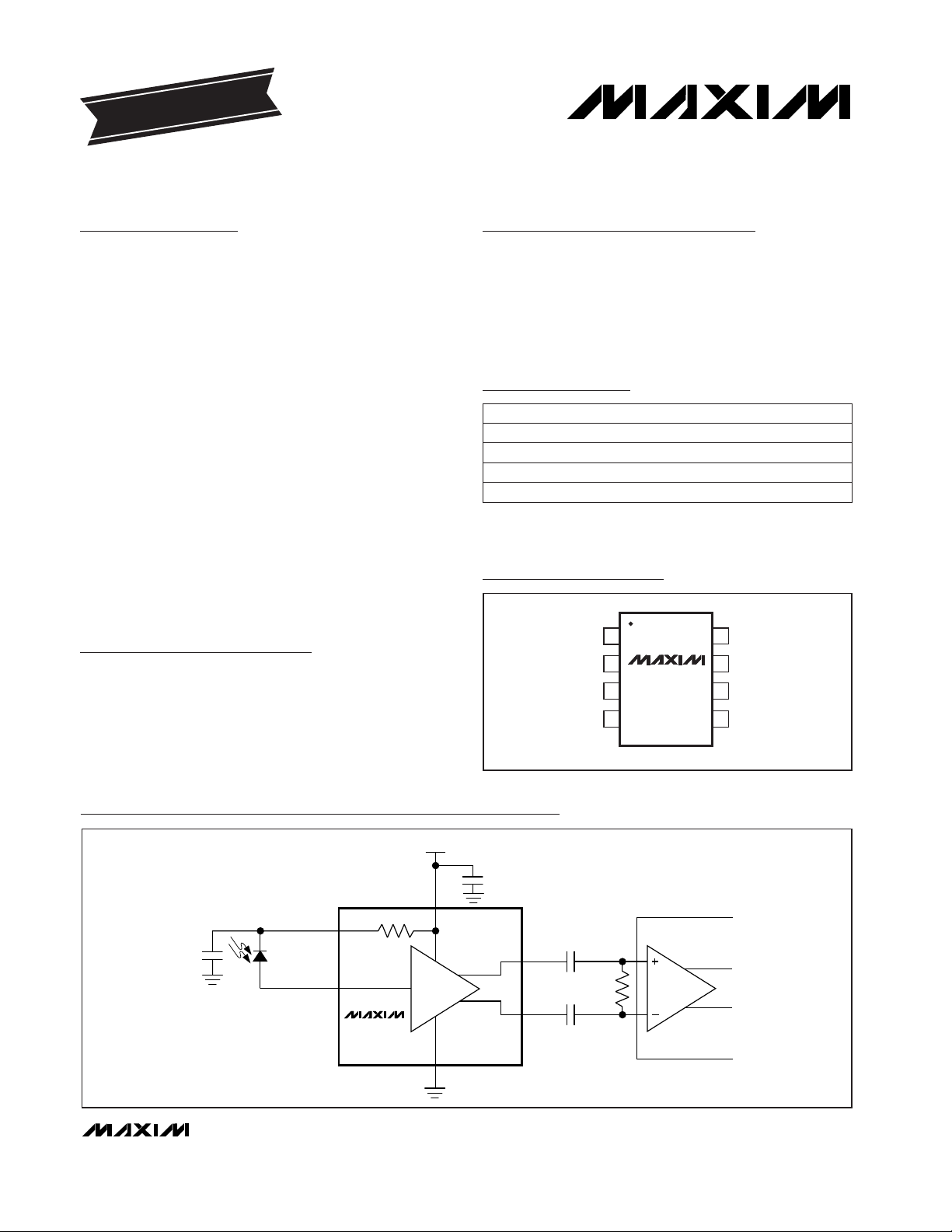
0.01µF
PHOTODIODE
1.5k
V
CC
V
CC
GND
FILTER
IN
0.1µF
OUT+
OUT-
0.1µF
C
FILTER
400pF
100Ω
MAX3266
MAX3267
LIMITING
AMPLIFIER
Typical Application Circuit
19-4796; Rev 0; 1/99
PART
MAX3266CSA
MAX3266C/D —
0°C to +70°C
TEMP. RANGE PIN-PACKAGE
8 SO
Dice*
EVALUATION KIT
AVAILABLE
*
Dice are designed to operate with junction temperatures of 0°C
to +100°C but are tested and guaranteed only at TA= +25°C.
Pin Configuration
Ordering Information
MAX3267CSA
MAX3267C/D —
0°C to +70°C 8 SO
Dice*
Page 2
ps
MAX3266/MAX3267
1.25Gbps/2.5Gbps, 3V to 5.5V, Low-Noise
Transimpedance Preamplifiers for LANs
2 _______________________________________________________________________________________
ABSOLUTE MAXIMUM RATINGS
ELECTRICAL CHARACTERISTICS
(VCC= +3.0V to +5.5V, TA= 0°C to +70°C, 100Ω load between OUT+ and OUT-. Typical values are at TA = +25°C, V
CC
= 3.3V,
source capacitance = 0.85pF, unless otherwise noted.) (Note 1)
Stresses beyond those listed under “Absolute Maximum Ratings” may cause permanent damage to the device. These are stress ratings only, and functional
operation of the device at these or any other conditions beyond those indicated in the operational sections of the specifications is not implied. Exposure to
absolute maximum rating conditions for extended periods may affect device reliability.
Supply Voltage (V
CC
- GND).................................-0.5V to +6.0V
IN Current..............................................................-4mA to +4mA
FILTER Current......................................................-8mA to +8mA
Voltage at OUT+, OUT-...................(V
CC
- 1.5V) to (V
CC
+ 0.5V)
Continuous Power Dissipation (T
A
= +70°C)
SO package (derate 6.7mW/°C above +70°C).............533mW
Storage Temperature Range.............................-55°C to +150°C
Operating Junction Temperature (die)..............-55°C to +150°C
Processing Temperature (die).........................................+400°C
Lead Temperature (soldering, 10sec).............................+300°C
MAX3267
MAX3266
MAX3267
MAX3266
MAX3267
MAX3266
MAX3266
MAX3267
MAX3266
Power-Supply Rejection Ratio
(PSRR)
50 dB
Output referred, f < 2MHz
PSRR = -20log (∆V
OUT
/∆VCC)
19 76
Transimpedance Linear Range
40
µAp-p
30
Low-Frequency Cutoff 44 kHz
750 920 1100
Small-Signal Bandwidth
1530 1900 2420
MHz
Peak-to-peak
0.95 < linearity < 1.05
-3dB, input ≤ 20µADC
6.6
Input-Referred RMS Noise
485 655
nA
200
DC Input Overload
AC Input Overload 1.0 mAp-p
0.65 mA
192 256
SO package
(Note 2)
Die, packaged in TO-56
header (Note 2)
PARAMETER MIN TYP MAX UNITS
Filter Resistor 1220 1500 1860 Ω
Output Impedance 48 50 52 Ω
Transimpedance
1540 1900 2330
Ω
Supply Current
Input Bias Voltage 0.69 0.83 0.91 V
26 50 mA
2260 2800 3400
CONDITIONS
Single-ended (per side)
Differential, measured
with 30µAp-p signal
(40µAp-p for MAX3267)
Note 1: Source Capacitance represents the total capacitance at the IN pin during characterization of noise and bandwidth parame-
ters. Figure 1 shows the typical source capacitance vs. reverse voltage for the photodiode used during characterization of
TO-56 header packages. Noise and bandwidth will be affected by the source capacitance. See the
Typical Operating
Characteristics
for more information.
Note 2: Input-Referred Noise is calculated as RMS Output Noise / (Gain at f = 10MHz). Noise Density is (Input-Referred Noise) /
√
bandwidth. No external filters are used for the noise measurements.
Note 3: Deterministic Jitter is measured with the K28.5 pattern applied to the input [00111110101100000101].
Maximum Differential Output
Voltage
185 250 415 mVp-pInput = 1mAp-p
MAX3266
MAX3267
Input-Referred Noise Density
11.0
pA/(Hz)
1/2
(Note 2)
Deterministic Jitter
12 50
ps(Note 3)
MAX3266
MAX3267
Page 3
MAX3266/MAX3267
1.25Gbps/2.5Gbps, 3V to 5.5V, Low-Noise
Transimpedance Preamplifiers for LANs
_______________________________________________________________________________________
3
170
180
190
200
210
220
230
240
250
0 255075100
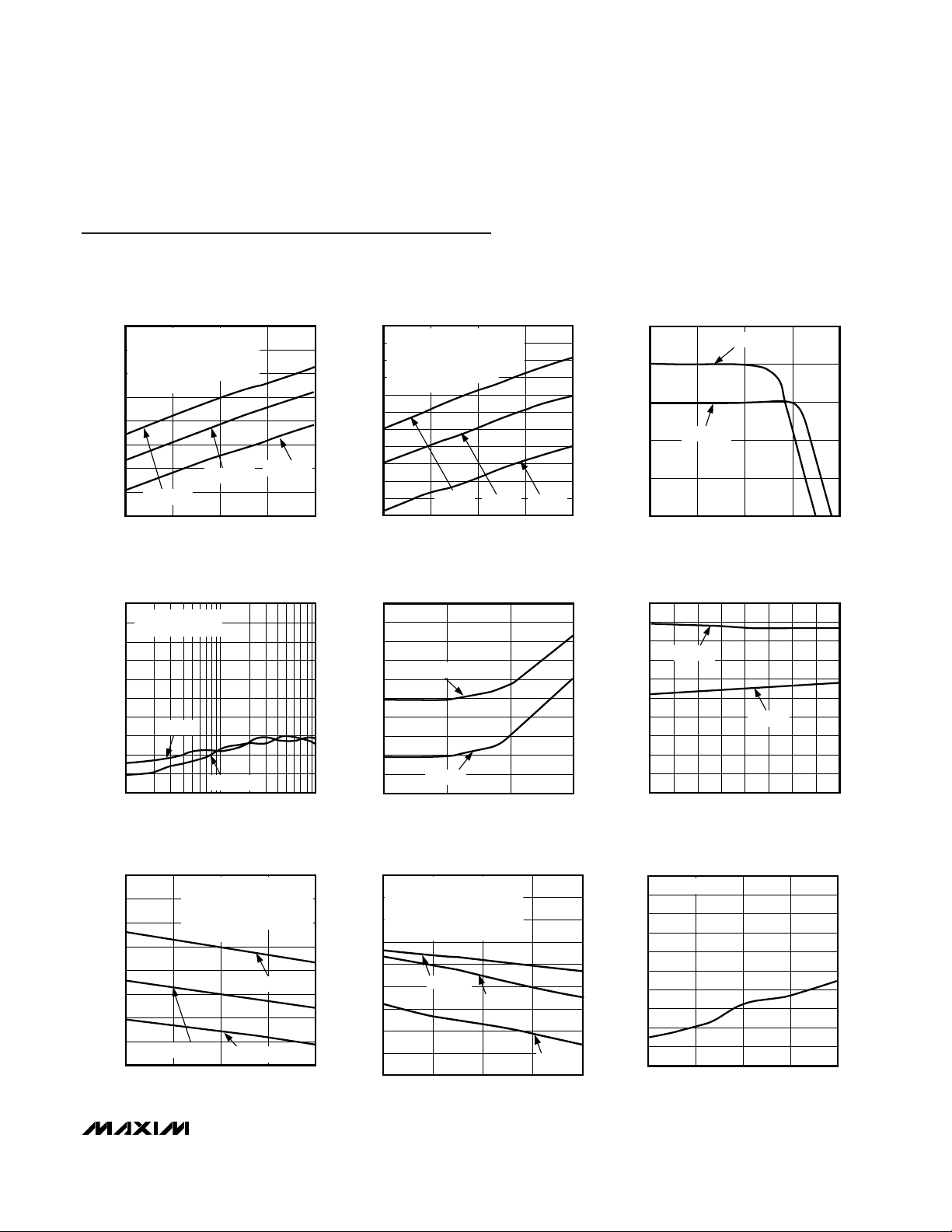
MAX3266
INPUT-REFERRED NOISE vs. TEMPERATURE
MAX3266/67-01
JUNCTION TEMPERATURE (°C)
INPUT-REFERRED NOISE (nA)
CIN = 1.5pF
CIN = 1.0pF
CIN = 0.5pF
CIN IS SOURCE CAPACITANCE
PRESENTED TO DIE, INCLUDES
PACKAGE PARASITIC, PIN DIODE,
AND PARASITIC INTERCONNECT
CAPACITANCE
420
440
460
480
500
520
540
560
580
600
620
640
0 255075100
MAX3267
INPUT-REFERRED NOISE vs. TEMPERATURE
MAX3267 toc02
JUNCTION TEMPERATURE (°C)
INPUT-REFERRED NOISE (nA)
CIN IS SOURCE CAPACITANCE
PRESENTED TO DIE, INCLUDES
PACKAGE PARASITIC, PIN DIODE,
AND PARASITIC INTERCONNECT
CAPACITANCE
CIN 1.5pF
CIN 1.0pF CIN 0.5pF
50
60
55
70
65
75
1M 10M 100M 1G 10G
FREQUENCY RESPONSE
MAX3266/67-03
FREQUENCY (Hz)
TRANSIMPEDANCE (dB)
MAX3267
MAX3266
100
0
10 100 1000
DETERMINISTIC JITTER
vs. INPUT AMPLITUDE
20
10
MAX3266/67-04
PEAK-TO-PEAK AMPLITUDE (µA)
PEAK-TO-PEAK JITTER (ps)
40
30
60
70
50
80
90
K28.5 DATA STREAM
EXTINCTION RATIO > 8
MAX3267
MAX3266
740
890
840
790
940
990
1040
1090
0 25 50 75 100
MAX3266
BANDWIDTH vs. TEMPERATURE
MAX3266/67-07
JUNCTION TEMPERATURE (°C)
BANDWIDTH (MHz)
CIN IS SOURCE CAPACITANCE
PRESENTED TO DIE, INCLUDES
PACKAGE PARASITIC, PIN DIODE,
AND PARASITIC INTERCONNECT
CAPACITANCE
CIN = 1.5pF
CIN = 1.0pF
CIN = 0.5pF
0
300
200
100
400
500
600
700
800
900
1000
1 10 100 1000
INPUT-REFERRED RMS NOISE CURRENT
vs. DC INPUT CURRENT
MAX3266/67-05
DIFFERENTIAL DC INPUT CURRENT (µA)
INPUT-REFERRED NOISE (nA)
MAX3267
MAX3266
60
63
62
61
64
65
66
67
68
69
70
01020304050607080
SMALL-SIGNAL TRANSIMPEDANCE
vs. TEMPERATURE
MAX3266/67-06
AMBIENT TEMPERATURE (°C)
TRANSIMPEDANCE (dB)
MAX3267
MAX3266
200
260
240
220
280
300
320
340
360
380
400
020406080
MAX3266/MAX3267
OUTPUT AMPLITUDE vs. TEMPERATURE
MAX3266/67-08
AMBIENT TEMPERATURE (°C)
AMPLITUDE (mV)
INPUT = 1mAp-p
Typical Operating Characteristics
(VCC= +3.3V, TA= +25°C, MAX3266/MAX3267 EV kit, source capacitance = 0.85pF, unless otherwise noted.)
1500
1700
1800
1900
2000
2100
2200
2300
2400
0 25 50 75 100
MAX3267
BANDWIDTH vs. TEMPERATURE
MAX3367 toc3
JUNCTION TEMPERATURE (°C)
BANDWIDTH (MHz)
1600
CIN IS SOURCE CAPACITANCE
PRESENTED TO DIE, INCLUDES
PACKAGE PARASITIC, PIN DIODE,
AND PARASITIC INTERCONNECT
CAPACITANCE
C
IN
= 1.5pF
C
IN
= 0.5pF
C
IN
= 1.0pF
Page 4

NAME FUNCTION
1 V
CC
Supply Voltage
PIN
Pin Description
2 N.C. No Connection
3 IN Amplifier Input
4 FILTER
Provides bias voltage for the photodiode through a 1.5kΩ resistor to VCC. When grounded, this pin disables
the DC Cancellation Amplifier to allow a DC path from IN to OUT+ and OUT- for testing.
5 GND Ground
6 OUT- Inverting Output. Current flowing into IN causes V
OUT-
to decrease.
7 OUT+ Noninverting Output. Current flowing into IN causes V
OUT+
to increase.
8 GND Ground
MAX3266/MAX3267
1.25Gbps/2.5Gbps, 3V to 5.5V, Low-Noise
Transimpedance Preamplifiers for LANs
4 _______________________________________________________________________________________
Typical Operating Characteristics (continued)
(VCC= +3.3V, TA= +25°C, MAX3266/MAX3267 EV kit, source capacitance = 0.85pF, unless otherwise noted.)
-150
-100
-50
0
50
100
150
-200 -100-150 -50 0 50 100 150 200
DC TRANSFER FUNCTION
MAX3266/67-13
INPUT CURRENT (µA)
OUTPUT VOLTAGE (mVp-p)
MAX3267
MAX3266
80ps/div
MAX3267
EYE DIAGRAM (INPUT = 1mAp-p)
MAX3266/67-12
30mV/div
INPUT: 27-1 PRBS
160ps/div
MAX3266
EYE DIAGRAM (INPUT = 1mAp-p)
MAX3266/67-10
30mV/div
INPUT: 27-1 PRBS
80ps/div
MAX3267
EYE DIAGRAM (INPUT = 20µAp-p)
MAX3266/67-11
5mV/div
INPUT: 27-1 PRBS
160ps/div
MAX3266
EYE DIAGRAM (INPUT = 10µAp-p)
MAX3266/67-09
4mV/div
INPUT: 27-1 PRBS
Page 5

MAX3266/MAX3267
1.25Gbps/2.5Gbps, 3V to 5.5V, Low-Noise
Transimpedance Preamplifiers for LANs
_______________________________________________________________________________________ 5
General Description
The MAX3266 is a transimpedance amplifier designed
for 1.25Gbps fiber optic applications. Figure 2 is a functional diagram of the MAX3266, which comprises a transimpedance amplifier, a voltage amplifier, an output
buffer, an output filter, and a DC cancellation circuit.
The MAX3267, a transimpedance amplifier designed
for 2.5Gbps fiber optic applications, shares similar
architecture with the MAX3266.
Transimpedance Amplifier
The signal current at the input flows into the summing
node of a high-gain amplifier. Shunt feedback through
RFconverts this current to a voltage with gain of approximately 2.2kΩ (1.0kΩ for MAX3267). Schottky diodes
clamp the output voltage for large input currents, as
shown in Figure 3.
Voltage Amplifier
The voltage amplifier converts single-ended signals to
differential signals and introduces a voltage gain.
Output Buffer
The output buffer provides a reverse-terminated voltage output. The buffer is designed to drive a 100Ω dif-
ferential load between OUT+ and OUT-. The output
current is divided between internal, 50Ω load resistors
and the external load resistor. In the typical operating
circuit, this creates a voltage divider with gain of 1/2.
The MAX3266 can also be terminated with higher output impedances, which increases gain and output voltage swing.
For optimum supply-noise rejection, the MAX3266
should be terminated with a differential load. If a singleended output is required, the unused output should be
similarly terminated. The MAX3266 will not drive a DCcoupled, 50Ω grounded load.
VOLTAGE
AMPLIFIER
TRANSIMPEDANCE
AMPLIFIER
OUTPUT
BUFFER
OUTPUT
FILTER
OUT+
50Ω
50Ω
OUT-
V
CC
R
F
V
CC
LOWPASS FILTER
1.5k
FILTER
IN
GND
DC CANCELLATION
CIRCUIT
DISABLE
MAX3266
Figure 2. MAX3266 Functional Diagram
0.50
0.95
0.80
0.65
1.10
1.25
1.40
1.55
1.70
1.85
2.00
021 345
MAX3266/67 fig01
REVERSE BIAS (V)
CAPACITANCE (pF)
Figure 1. Typical Photodiode Capacitance vs. Bias Voltage
Page 6

MAX3266/MAX3267
1.25Gbps/2.5Gbps, 3V to 5.5V, Low-Noise
Transimpedance Preamplifiers for LANs
6 _______________________________________________________________________________________
Output Filter
The MAX3266 includes a 1-pole lowpass filter which
limits the circuit bandwidth and improves noise performance.
DC Cancellation Circuit
The DC cancellation circuit uses low-frequency feedback to remove the DC component of the input signal
(Figure 4). This feature centers the input signal within
the transimpedance amplifier’s linear range, thereby
reducing pulse-width distortion on large input signals.
The DC cancellation circuit is internally compensated
and therefore does not require external capacitors. This
circuit minimizes pulse-width distortion for data
sequences that exhibit a 50% duty cycle. A duty cycle
significantly different from 50% will cause the MAX3266
to generate pulse-width distortion.
DC cancellation current is drawn from the input and
creates noise. For low-level signals with little or no DC
component, this is not a problem. Amplifier noise will
increase for signals with significant DC component (see
Typical Operating Characteristics
).
Applications Information
Optical Power Relations
Many of the MAX3266 specifications relate to the input
signal amplitude. When working with fiber optic
receivers, the input is usually expressed in terms of average optical power and extinction ratio. Figure 5 shows
relations that are helpful for converting optical power to
input signal when designing with the MAX3266.
Optical power relations are shown in Table 1; the definitions are true if the average duty cycle of the input data
is 50%.
Optical Sensitivity Calculation
The input-referred RMS noise current (IN) of the
MAX3266 generally determines the receiver sensitivity.
To obtain a system bit error rate (BER) of 1E-12, the
signal-to-noise ratio must always exceed 14.1. The
input sensitivity, expressed in average power, can be
estimated as:
Where ρ is the photodiode responsivity in A/W.
Input Optical Overload
The overload is the largest input that the MAX3266
accepts while meeting specifications. The optical overload can be estimated in terms of average power with
the following equation:
Overload
mA
dBm log =
10
1
2
1000
ρ
Sensitivity
Ir
r
dBm
Ne
e
=
+
()
−
()
10
14 1 1
21
1000log
.
ρ
AMPLITUDE
OUTPUT (LARGE SIGNALS)
TIME
OUTPUT (SMALL SIGNALS)
Figure 3. MAX3266 Limited Output Figure 4 . DC Cancellation Effect On Input
AMPLITUDE
INPUT FROM PHOTODIODE
TIME
INPUT (AFTER DC CANCELLATION)
Page 7

MAX3266/MAX3267
1.25Gbps/2.5Gbps, 3V to 5.5V, Low-Noise
Transimpedance Preamplifiers for LANs
_______________________________________________________________________________________ 7
Optical Linear Range
The MAX3266 has high gain, which limits the output
when the input signal exceeds 30µAp-p (40µAp-p for
MAX3267). The MAX3266 operates in a linear range for
inputs not exceeding:
Layout Considerations
Use good high-frequency design and layout techniques. The use of a multilayer circuit board with separate ground and power planes is recommended.
Connect the GND pins to the ground plane with the
shortest possible traces.
Noise performance and bandwidth will be adversely
affected by capacitance at the IN pin. Minimize capacitance on this pin and select a low-capacitance photodiode. Assembling the MAX3266 in die form using chip
and wire technology provides the best possible performance. Figure 6 shows a suggested layout for a TO
header.
The SO package version of the MAX3266 is offered as
an easy way to characterize the circuit and become
familiar with the circuit’s operation, but it does not offer
optimum performance. When using the SO version of
the MAX3266, the package capacitance adds approximately 0.3pF at the input. The PC board between the
MAX3266 input and the photodiode also adds parasitic
capacitance. Keep the input line short, and remove
power and ground planes beneath it.
Photodiode Filter
Supply voltage noise at the cathode of the photodiode
produces a current I = CPD∆V/∆t, which reduces the
receiver sensitivity (CPDis the photodiode capacitance.) The filter resistor of the MAX3266, combined
with an external capacitor, can be used to reduce this
noise (refer to the
Typical Application Circuit
). Current
generated by supply noise voltage is divided between
C
FILTER
and CPD. The input noise current due to supply
noise is (assuming the filter capacitor is much larger
than the photodiode capacitance):
I
NOISE
= (V
NOISE
)(CPD) / (R
FILTER
)(C
FILTER
)
If the amount of tolerable noise is known, the filter
capacitor can be easily selected:
C
FILTER
= (V
NOISE
)(CPD) / (R
FILTER
)(I
NOISE
)
For example, with maximum noise voltage = 100mVp-p,
CPD= 0.85pF, R
FILTER
= 1.5kΩ, and I
NOISE
selected to
be 100nA (1/2 of the MAX3266’s input noise):
C
FILTER
= (100mV)(0.85pF) / (1500Ω)(100nA) = 570pF
Wire Bonding
For high current density and reliable operation, the
MAX3266 uses gold metalization. Connections to the
die should be made with gold wire only, using ball
bonding techniques. Wedge bonding is not recommended. Die thickness is typically 15 mils (0.375mm).
Linear Range
Ar
r
dBm
e
e
log
=
+
()
−
()
10
30 1
21
1000
µ
ρ
Figure 5. Optical Power Relations
PO
PI
P
AVE
TIME
OPTICAL POWER
PARAMETER
Average Power
Extinction Ratio
Optical Power
of a “1”
P1
r
e
P
AVE
SYMBOL RELATION
P
AVE
= (P0 + P1)/2
re= P1/P0
P1 = 2P
AVE (re
) / (re+ 1)
Optical Power
of a “0”
P0 P0 = 2P
AVE
/ (re+ 1)
Signal
Amplitude
P
IN
PIN= P1 - P0
= 2P
AVE (re
) / (re+ 1)
Table 1. Optical Power Relations
Page 8

MAX3266/MAX3267
1.25Gbps/2.5Gbps, 3V to 5.5V, Low-Noise
Transimpedance Preamplifiers for LANs
Figure 6. Suggested Layout for TO-56 Header
CASE IS GROUND
TOP VIEW OF TO-56 HEADER
C
FILTER
V
CC
PHOTODIODE
MAX3266/MAX3267
OUT+
OUT-
Chip Topographies
0.50"
(1.25mm)
0.030"
(0.75mm)
GND
OUT-
FILTER
INPUT
V
CC
GND
OUT+
0.50"
(1.25mm)
0.030"
(0.75mm)
GND
OUT-
FILTER
INPUT
V
CC
GND
OUT+
MAX3266
MAX3267
TRANSISTOR COUNT: 320
SUBSTRATE CONNECTED TO GND
Maxim cannot assume responsibility for use of any circuitry other than circuitry entirely embodied in a Maxim product. No circuit patent licenses are
implied. Maxim reserves the right to change the circuitry and specifications without notice at any time.
8
_____________________Maxim Integrated Products, 120 San Gabriel Drive, Sunnyvale, CA 94086 408-737-7600
© 1999 Maxim Integrated Products Printed USA is a registered trademark of Maxim Integrated Products.
 Loading...