

Page 1
________________General Description
The MAX3262 limiting amplifier with its high gain and
wide bandwidth is ideal for use as a post amplifier in
fiber-optic receivers with data rates up to 1Gbps. The
amplifier’s gain can be adjusted between 33dB and
48dB. At maximum gain, signals as small as 6mVp-p
can be amplified to drive devices with PECL inputs.
The MAX3262 has complementary loss-of-signal outputs for interfacing with open-fiber-control (OFC) circuitry. These outputs can be programmed to assert
with input levels between 9mVp-p and 48mVp-p. LOS
hysteresis for any programmed level is nominally
3.0dB, preserving a balance between noise immunity
and dynamic range.
________________________Applications
1062Mbps Fibre Channel
622Mbps SONET
____________________________Features
♦ 900MHz Bandwidth
♦ 48dB Maximum Gain
♦ Chatter-Free LOS
♦ Programmable LOS Threshold
♦ Single +5V Power Supply
♦ Fully Differential Architecture
_______________Ordering Information
MAX3262
1Gbps, High-Speed Limiting Amplifier with
Chatter-Free Loss-of-Signal Detection
________________________________________________________________
Maxim Integrated Products
1
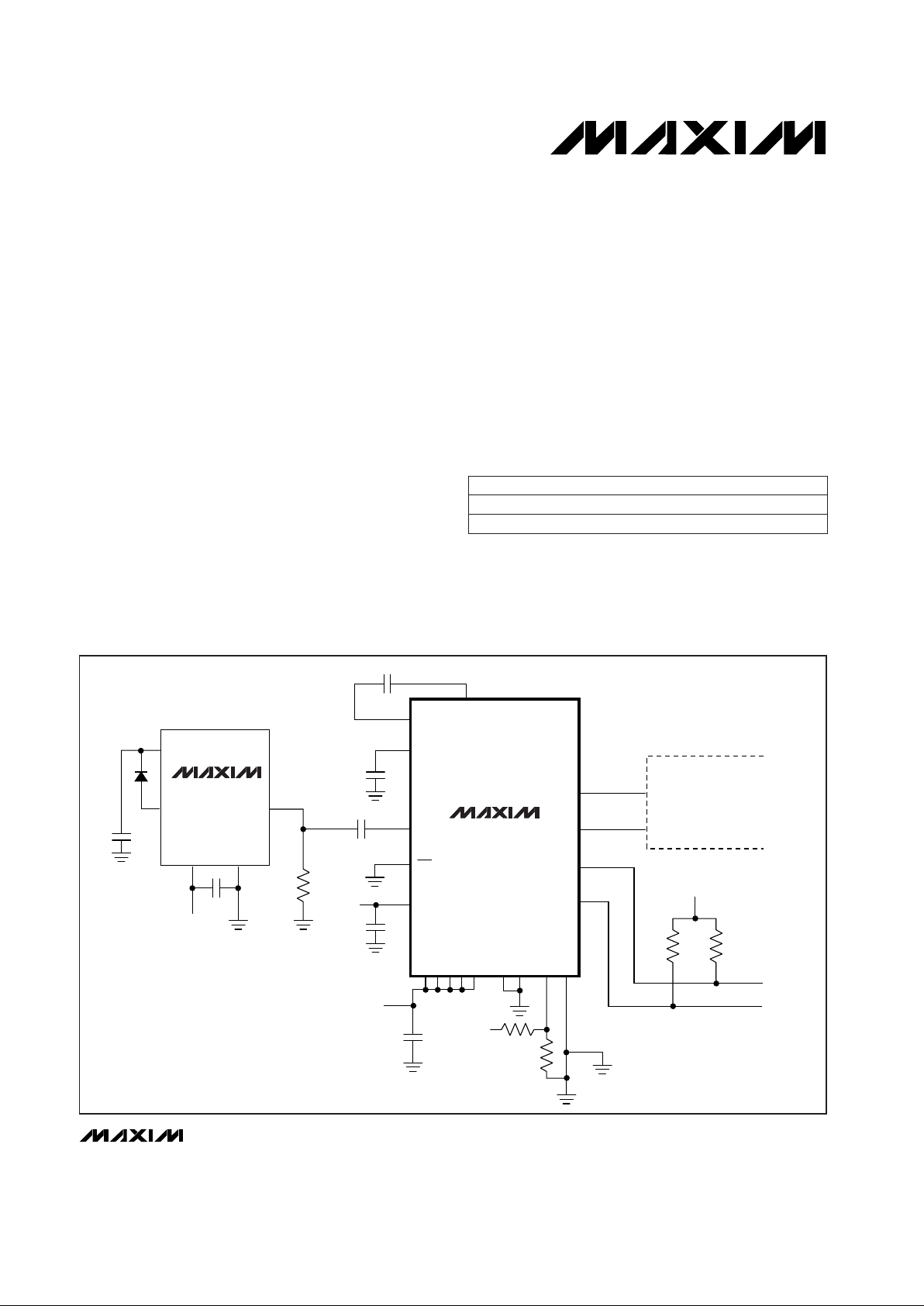
MAX3262
MAX3260
0.01µF
V
CC
ENB
DIN-
DIN+
RECEIVER WITH
PECL TERMINATIONS
(50Ω TO V
CC
- 2V)
DOUT-
DOUT+
LOSB
GND
OUTPUT
C
IN
C
IN
INPUT
FILTER
LOS
LOSB
LOS
CZN
CZP
V
CC
GND
C
AZ
+5V
+5V
50Ω +5V
+5V
+5V
C1
0.01µF
C1
R2
R1
R
4.7k
R
4.7k
V
CC
A
V
CC
B
V
CC
C
V
CC
D
V
CC
E
V
LOS
DIV2
____________________________________________________Typical Operating Circuit
19-0324; Rev 2; 12/97
PART
MAX3262CAG 0°C to +70°C (T
A
)
TEMP. RANGE PIN-PACKAGE
24 SSOP
Pin Configuration appears at end of data sheet.
MAX3262C/D 0°C to +100°C (TJ) Dice*
For free samples & the latest literature: http://www.maxim-ic.com, or phone 1-800-998-8800.
For small orders, phone 408-737-7600 ext. 3468.
*Dice are designed to operate over this range but are tested and
guaranteed only at TA= +25°C.
Page 2
MAX3262
1Gbps, High-Speed Limiting Amplifier with
Chatter-Free Loss-of-Signal Detection
2 _______________________________________________________________________________________
ABSOLUTE MAXIMUM RATINGS
DC ELECTRICAL CHARACTERISTICS
(VCC= +5V, R
LOAD
= 50Ω to VCC- 2V (equivalent), TA= 0°C to +70°C. Typical values are at VCC= 5V and TA= +25°C.)
AC ELECTRICAL CHARACTERISTICS
(VCC= +5V, R
LOAD
= 50Ω to 3V, AC parameters are not tested, TA= +25°C, unless otherwise noted.)
Stresses beyond those listed under “Absolute Maximum Ratings” may cause permanent damage to the device. These are stress ratings only, and functional
operation of the device at these or any other conditions beyond those indicated in the operational sections of the specifications is not implied. Exposure to
absolute maximum rating conditions for extended periods may affect device reliability.
Note 1: Input is a 200MHz square wave, tR< 300ps, 8mVp-p.
Note 2: Input is a 200MHz square wave, t
R
< 300ps, 1.8Vp-p.
Note 3: Input-referred noise = RMS output noise/low-frequency gain.
Power Supply, V
CC
- VEE......................................................6.0V
Input Voltage, DIN+, DIN-.....................................................6.0V
CZN, CZP, ENB, VLOS, DIV2, LOS+, LOS-.....-0.3V, V
CC
+ 0.3V
DOUT+, DOUT- (with 50Ω load).......................2.5V, V
CC
+ 0.3V
Continuous Power Dissipation (T
A
= +70°C)
SSOP (derate 10mW/°C above +70°C) ....................500mW°C
Junction Operating Temperature ......................-55°C to +150°C
Storage Temperature Range.............................-55°C to +175°C
Processing Temperature (Die).........................................+400°C
No output load
VCC= 5.0V
I
OUT
= -1.0mA
DIV2 = 0V
CONDITIONS
µA150I
ENB
Enable Input Current
mA60I
VCC
Power-Supply Current
V2.5 3.0V
DIN
Input Bias Voltage
µA120I
LOS
V
LOS
Input Current
V3.5 3.7 3.8Common-Mode Output Voltage
V0.5
LOS+, LOS- Output Low
Voltage
mA0.5DIV2 Short-Circuit Current
UNITSMIN TYP MAXSYMBOLPARAMETER
mV±35
Differential Output Offset,
DOUT+ to DOUT-
MAX3262CAG
MHz
MAX3262C/D
V
OH
- V
OL
1Gbps, 8mVp-p input
V
LOS
= 5V, DIV2 = GND (Note 3)
V
LOS
= 5V, Pattern 27 - 1PRBS
750 810
Peak-to-peak
(Note 1)
(Note 2) µs
Input referred, 55MHz
CONDITIONS
BWSmall-Signal Bandwidth
Differential inputs,
peak-to-peak
mV
10 48
V
SR
LOS Sensitivity Range
800 925
mV400 600 730V
OUT
Output Voltage Amplitude
ps250t
R, tF
Output Edge Speed
ps40PWDPulse-Width Distortion
µV80V
n
Differential Input Noise
dB1.5 3.0 5.0HYSLOS Hysteresis
V
9 48MAX3262C/D
MAX3262CAG
µs0.020 0.5t
OFFL
LOS Release Time,
Minimum Input
0.5t
OFFH
LOS Release Time,
Maximum Input
(Note 1)
dB35PSRRPower-Supply Rejection Ratio
µs0.2 0.5t
ONL
LOS Assert Time
UNITSMIN TYP MAXSYMBOLPARAMETER
0.006 1.8V
ID
Input Voltage Range
Page 3
MAX3262
1Gbps, High-Speed Limiting Amplifier with
Chatter-Free Loss-of-Signal Detection
_______________________________________________________________________________________
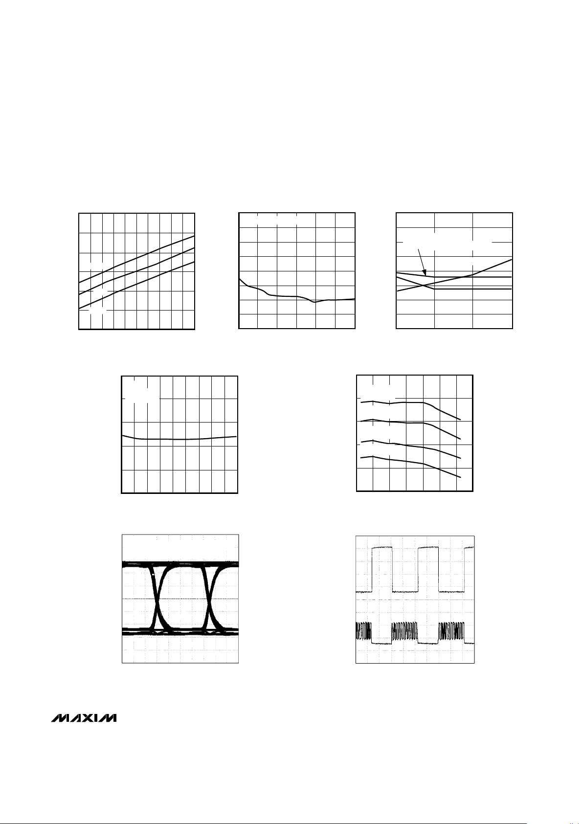
3
70
65
60
55
50
45
40
VCC SUPPLY CURRENT
(NO OUTPUT LOAD) vs. TEMPERATURE
MAX3262-01
SUPPLY CURRENT (mA)
0 10 20 30 40 50 60 70 80 90 100
TEMPERATURE (°C)
5.25V
5.0V
4.75V
0
0
LOS HYSTERESIS
vs. TEMPERATURE
MAX3262-02
TEMPERATURE (°C)
HYSTERESIS (dB)
20 40 60 80 100 120
1
2
3
4
5
6
7
8
1Gbps WITH 1,0 PATTERN
4.0
400
LOS SENSITIVITY
vs. FREQUENCY
MAX3262-03
FREQUENCY (Mbps)
SENSITIVITY (mVp-p)
600 800 1000
4.5
5.0
5.5
6.0
6.5
7.0
7.5
8.0
1-0 PATTERN
K28.5 SEQUENCE
(FIBRE CHANNEL IDLE PATTERN)
PRBS 27-1
4.0
3.0
2.0
1.0
0
3.2 3.4 3.6 3.8 4.0 4.2 4.4 4.6 4.8 5.0
LOS HYSTERESIS vs. V
LOS
MAX3262-04
V
LOS
(V)
5.0
HYSTERESIS (dB)
1Gbps
DIV2 = 0
1,0 PATTERN
25
0
FREQUENCY RESPONSE
MAX3262-05
FREQUENCY (MHz)
GAIN (dB)
200 400 600 800 1000 1200 1400
31
37
43
49
55
V
LOS
= 5V
DIV2 = GND
V
LOS
= 5V
DIV2 OPEN
V
LOS
= 3.4V
DIV2 OPEN
V
LOS
= 3.0V
DIV2 OPEN
EYE DIAGRAM
1Gbps
R
LOAD
= 50Ω to VCC - 2V (EQUIVALENT)
V
IN
= 250mV, V
CC
= +5V, DIV2 = GND, V
LOS
= V
CC
V
LOS
= V
CC
MAX3262-07
+500mV
100mV/div
-500mV
225ps/div
LOS
OUTPUT
DATA
INPUT
LOS OPERATION
MAX3262-06
2µs/div
__________________________________________Typical Operating Characteristics
(VCC= 5V, TA = +25°C, unless otherwise noted.)
Page 4

MAX3262
1Gbps, High-Speed Limiting Amplifier with
Chatter-Free Loss-of-Signal Detection
4 _______________________________________________________________________________________
_______________________________________________________________Pin Description
NAME FUNCTION
1 VCCB Positive supply for internal gain stages
PIN
5 VCCA Power supply for the input stage amplifier
6 DIN+ Data Input
10 DIV2
Input stage gain adjust. Grounding this pin forces the input stage gain to maximum (11dB) for applications
where the LOS threshold level will be set for input signals in the 9mVp-p to 20mVp-p range. Leaving this pin
open forces the gain of the input stage to be divided by two (6dB) for applications where the LOS threshold
level will be set for input signal levels in the 15mVp-p to 48mVp-p range.
9
ENB
Output Enable. Output gain stage is disabled and LOS circuitry remains functional.
8 GND Ground for the input stage amplifier
7 DIN- Inverting Data Input
15 VCCD Positive supply for the LOS+/LOS- buffer circuitry
14 GND Ground for the LOS+/LOS- buffer circuitry
13 GND Ground for the power detect/LOS circuitry
12 VCCE Positive supply for the power detect/LOS circuitry
11 VTH Comparator threshold voltage for test only. Leave unconnected.
19 DOUT+ Data Output
18 DOUT- Inverting Data Output
17 LOS+ Loss-of-Signal detect. This pin is asserted high when input power drops below the LOS threshold level.
16 LOS- Loss-of-Signal detect. This pin is asserted low when input power drops below the LOS threshold level.
23 V
CC
Positive supply for output buffers
22 GND Ground for bias generators
21 VCCC Positive supply for bias generators
20 GND Substrate Ground
24 GND Ground for internal gain stages
4 CZN
Offset-correction loop compensation capacitor. This pin should be connected to the CZP pin through a
100nF to 330nF capacitor, which provides the dominant pole for the offset-correction loop.
2 V
LOS
Power detect/LOS level set. Use this input to program the required threshold level for LOS assertion.
3 CZP
Offset-correction loop compensation capacitor. This pin should be connected to the CZN pin through a
100nF to 330nF capacitor, which provides the dominant pole for the offset-correction loop.
Page 5

_______________Detailed Description
The MAX3262 is an integrated limiting amplifier intended for high-frequency fiber-optic applications. The circuit connects to typical transimpedance amplifiers
found within a fiber-optic link. The linear signal output
from a transimpedance amplifier can contain significant
amounts of noise, and may vary in amplitude over time.
The MAX3262 limiting amplifier quantizes the signal,
and outputs a voltage-limited waveform over a 48dB
input dynamic range.
The MAX3262 provides an offset correction function
that effectively reduces the offset voltage to negligible
levels. In communications systems using NRZ data with
a 50% duty cycle, pulse-width distortion present in the
signal or generated by the transimpedance amplifier
appears as input offset and is partially removed by the
offset correction function. An external capacitor is
required between CZP and CZN to compensate the offset correction loop, determining the lower 3dB point.
Loss-of-Signal Function
The MAX3262 incorporates a chatter-free loss-of-signal
function, which is used to detect that the input signal
has dropped below the level necessary for acceptable
bit error rate performance, or to indicate an open-fiber
condition. The loss-of-signal function is implemented
with a rectifying peak detector, which samples the signal entering the output stage. The output from the peak
detector is compared against an internally generated
threshold, and is used to assert the LOS+ and LOSoutputs.
The loss-of-signal threshold is adjusted by varying the
amplifier gain. The MAX3262 is configurable for gains
between 33dB and 48dB, allowing LOS thresholds
between 9mVp-p and 48mVp-p. Figure 2 shows the
LOS threshold as a function of the DIV2 and V
LOS
pins.
The DIV2 pin provides a coarse adjustment of 6dB of
gain, while the V
LOS
pin provides a fine gain adjust-
ment between 0dB and 11dB.
MAX3262
1Gbps, High-Speed Limiting Amplifier with
Chatter-Free Loss-of-Signal Detection
_______________________________________________________________________________________ 5
DIN-
DIV2
DIN+
20k
20k
DOUT-
ENB
DOUT+
RMS
DETECT
BIAS
REFERENCE
LOS+
LOS-
C
AZ
OFFSET
CORRECTION
V
LOS
MAX3262
0dB to 11dB5dB/11dB 10dB 10dB 6dB
Figure 1. Functional Diagram
Page 6

MAX3262
Level-detect hysteresis and a 200ns internal delay
ensure chatter-free LOS outputs when the input signal
level is close to the LOS threshold. The hysteresis for
any programmed loss-of-signal level is nominally 2.5dB.
The LOS+ and LOS- outputs are open-collector,
Schottky-clamped transistors, that require pull-up resistors for proper operation (Figure 3). The loss-of-signal
time constant is set externally with the appropriate pull-up
resistor and shunt load capacitance.
The ENB pin allows the user to disable the output signal without removing the input signal.
Wire Bonding Die
For reliable operation, the MAX3262 has gold metalization. Connections to the die should be made with gold
wire only, using ball bonding techniques. Wedge bonding is not recommended. Bond pad size is 4 mils.
__________________Design Procedure
Determining Capacitor Values
The MAX3262 inputs must be AC coupled to allow proper operation of the offset correction function. Figure 4
shows the circuit’s input stage. The circuit’s lower -3dB
point is determined by the input coupling capacitors. The
lower -3dB frequency is 1 / [(2π)(1500Ω)(CIN)] Hz.
C
IN
should be large enough to not affect the signal
quality, but small enough to not affect the LOS assert
time. When an open-fiber condition occurs, the input
coupling capacitors must discharge below the LOS
threshold level before the LOS can assert. The worstcase discharge time would occur with the maximum
input signal and the minimum LOS threshold. In this
case, the input capacitor must discharge from 0.9V to
4.5mV. The time required for this to occur is:
t = (1500)(CIN) In(V
MAX
/ V
THRESH
) seconds
Example: If the MAX3262 is configured for 6mV sensitivity, CIN= 100pF results in a lower -3dB frequency of
1MHz, and a maximum LOS delay of about 1µs.
The offset correction capacitor (CAZ) must be greater
than 100nF to ensure stable operation. This capacitor is
in series with an internal 40kΩ of resistance. The -3dB
point of the offset zeroing circuit is:
1 / [(2π)(CAZ)(40kΩ)] Hz
For CAZ= 180nF, the bandwidth of the offset correction
circuit is 22Hz. Maxim’s proprietary offset-correction
architecture decouples the input coupling time constant
from the offset correction time constant. This ensures
there is no interaction between these two networks, eliminating an additional source of chatter on LOS.
1Gbps, High-Speed Limiting Amplifier with
Chatter-Free Loss-of-Signal Detection
6 _______________________________________________________________________________________
0
3.0 3.3 3.6 3.9 4.2 4.5 4.8 5.1
LOS ASSERT LEVEL
MAX3262-07
V
LOS
(V)
SENSITIVITY (mVp-p)
10
5
15
25
20
30
35
40
45
50
DIV2 OPEN
DIV2 GROUNDED
VCC = 5V
Figure 2. MAX3262 Sensitivity vs. V
LOS
Setting
MAX3262
LOS
BUFFER
LOS+
C
LOS
R
LOS
R
LOS
≥ 3.3kΩ
LOS OUTPUT WITH
DESIRED RISE TIME
+5V
Figure 3. Setting the LOS Time Constant
Page 7

Output Termination
The MAX3262 outputs must be terminated with a 50Ω
load to (VCC- 2V), or a Thevenin equivalent. Figure 5
shows two possible output termination methods.
Layout and PC Board Design
Since the MAX3262 is a high-frequency component,
the circuit’s performance can largely be determined by
board layout and design. A common problem with
high-gain amplifiers is feedback from the large swing
outputs to the input via the power supply. Some fiberoptic limiting amplifiers suffer from LOS “chatter.” The
act of switching the LOS outputs on or off generates
noise on the power supply, which can cause the LOS
outputs to chatter. With proper board layout, the
MAX3262 ensures chatter-free LOS operation.
The MAX3262 has five ground pins and a substrate
connection. All of these should be connected to the circuit board’s ground. Use multiple PCB vias close to the
part to connect the grounds. Avoid long, inductive runs,
which can degrade MAX3262 performance. The
MAX3262’s six VCCsupply pins must all be connected.
VCCA–VCCE can be collectively decoupled with one
capacitor. VCC(pin 23) should be decoupled separately (see the
Typical Operating Circuit
).
MAX3262
1Gbps, High-Speed Limiting Amplifier with
Chatter-Free Loss-of-Signal Detection
_______________________________________________________________________________________ 7
C
IN
V
IN
C
IN
DIN+
DIN-
V
CC
1.5k
1.5k
MAX3262
DOUT+
+5V
+5V
b) DRIVING A HIGH-IMPEDANCE LOAD
Z
LOAD
>500Ω
DOUT-
82Ω
120Ω
82Ω
120Ω
MAX3262
DOUT+
a) DRIVING A 50Ω LOAD TO GROUND
50Ω
DOUT-
50Ω
330Ω
330Ω
MAX3262
Figure 4. MAX3262 Equivalent Input Circuit
Figure 5. Output Termination Techniques
Page 8

MAX3262
1Gbps, High-Speed Limiting Amplifier with
Chatter-Free Loss-of-Signal Detection
___________________Pin Configuration ____________________Chip Topography
24
23
22
21
20
19
18
17
1
2
3
4
5
6
7
8
GND
V
CC
GND
V
CC
C
CZN
CZP
V
LOS
VCCB
TOP VIEW
GND
DOUT+
DOUT-
LOS+
GND
DIN-
DIN+
V
CC
A
16
15
14
13
9
10
11
12
LOSV
CC
D
GND
GND
V
CC
E
VTH
DIV2
ENB
SSOP
MAX3262
0.080"
(2.032mm)
0.060"
(1.524mm)
CZN
VCCA
DIV2
V
CC
C
GND
DOUT+
DOUT-
LOS+
LOS-
GND
VCCB
V
LOS
CZP
GND
V
CC
DIN+ DIN- GND
ENB
VTH
VCCE
GND
GND
VCCD
TRANSISTOR COUNT: 200
SUBSTRATE CONNECTED TO GND PIN 17
Maxim makes no warranty, representation, or guarantee regarding the suitability of its products for any particular purpose, nor does Maxim assume any liability arising out of the application or use of any product or circuit, and Maxim specifically disclaims any and all liability including, without limitation, consequential or incidental damages. “Typical’’ parameters can and do vary in different applications. All operating parameters, including “typicals”, must be
validated for each customer application by customer’s technical experts. Maxim products are not designed, intended, or authorized for use as components
in systems intended for surgical implant into the body, or other applications intended to support or sustain life, or for any other application in which the failure of the Maxim product could create a situation where personal injury or death may occur.
8
_____________________Maxim Integrated Products, 120 San Gabriel Drive, Sunnyvale, CA 94086 408-737-7600
© 1997 Maxim Integrated Products Printed USA is a registered trademark of Maxim Integrated Products.
 Loading...