

Page 1
For free samples & the latest literature: http://www.maxim-ic.com, or phone 1-800-998-8800.
For small orders, phone 408-737-7600 ext. 3468.
_______________General Description
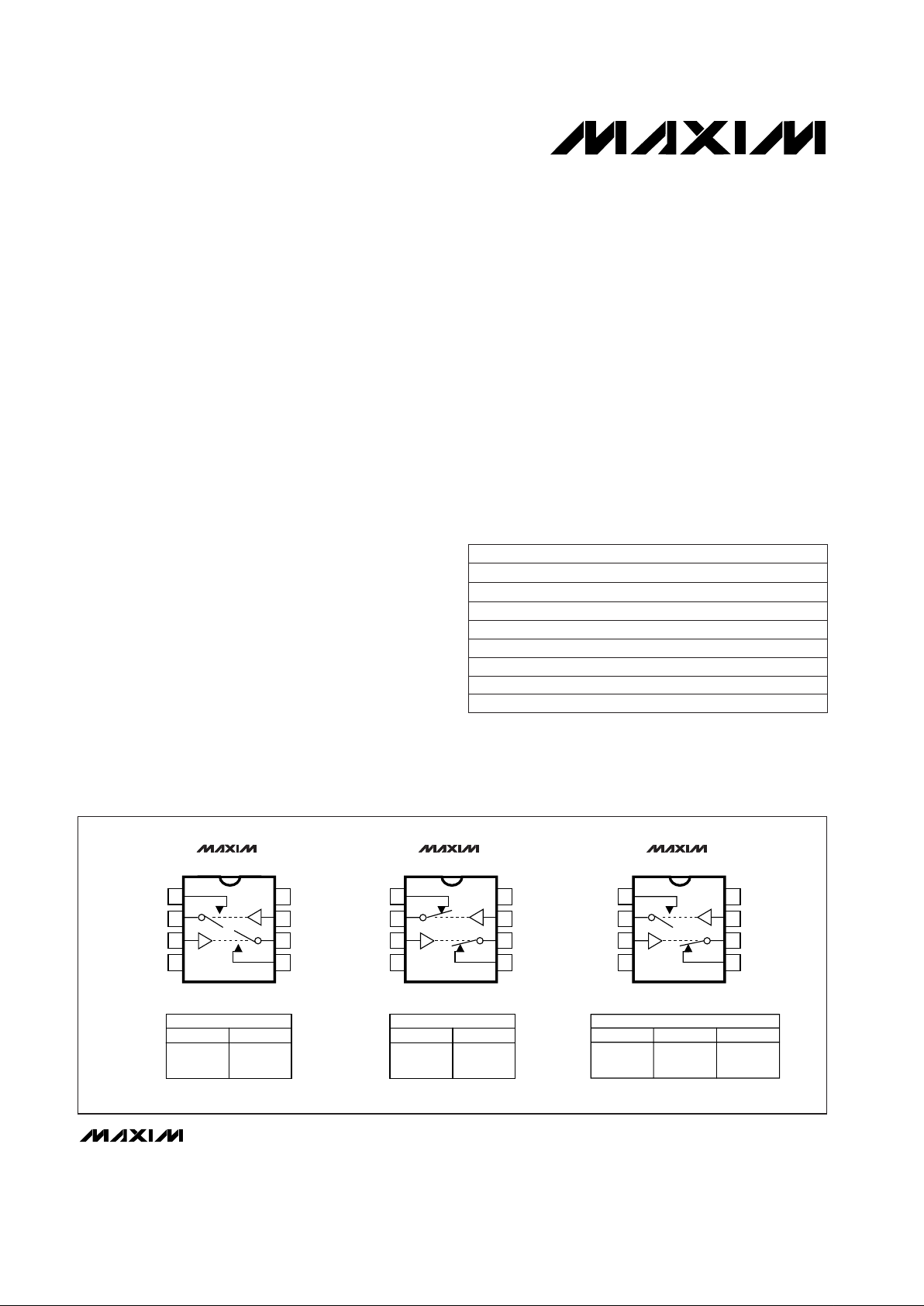
The MAX323/MAX324/MAX325 are precision, dual,
SPST analog switches. They are single-supply devices
designed to operate from +2.7V to +16V. The MAX323
has two normally open (NO) switches, and the MAX324
has two normally closed (NC) switches. The MAX325
has one NO and one NC switch. Low power consumption (5µW) makes these parts ideal for battery-powered
equipment. These switches offer low leakage currents
(100pA max) and fast switching speeds (tON= 150ns
max, t
OFF
= 100ns max).
When powered from a 5V supply, the MAX323 series
offers 2Ω max matching between channels, 60Ω max
on-resistance, and 6Ω max RONflatness.
These switches also offer 5pC max charge injection,
and a minimum of 2000V ESD per Method 3015.7.
For equivalent devices specified for dual-supply operation, see the MAX320/MAX321/MAX322 data sheet. For
quad versions of the MAX320 series, see MAX391/
MAX392/MAX393 data sheet.
________________________Applications
Battery-Operated Systems Sample-and-Hold Circuits
Heads-Up Displays Guidance and Control Systems
Audio and Video Switching Military Radios
Test Equipment Communications Systems
+3V, +5V DACs and ADCs PBX, PABX
____________________________Features
♦ Low On-Resistance (RON), 60Ω max (33Ω typ)
♦ RONMatching Between Channels <2Ω
♦ RONFlatness <6Ω Max
♦ Guaranteed Charge Injection <5pC
♦ Single-Supply Operation (+2.7V to +16V)
♦ Low Power Consumption, <5µW
♦ Low Leakage Current Over Temperature,
<2.5nA at +85°C
♦ Fast Switching: tON<150ns, t
OFF
<100ns
♦ Guaranteed Break-Before-Make (MAX325 only)
♦ TTL/CMOS Logic Compatible
______________Ordering Information
MAX323/MAX324/MAX325
Precision, Single-Supply,
SPST Analog Switches
________________________________________________________________
Maxim Integrated Products
1
DIP/SO/µMAX
8
7
6
5
1
2
3
4
V+
IN1
COM2
NC2
V-
IN2
COM1
NC1
MAX324
DIP/SO/µMAX
8
7
6
5
1
2
3
4
V+
IN1
COM2
NC2
V-
IN2
COM1
NO1
MAX325
SWITCHES SHOWN FOR LOGIC "0" INPUT
MAX324
LOGIC SWITCH
0
1
ON
OFF
TOP VIEW
DIP/SO/µMAX
MAX323
LOGIC SWITCH
0
1
OFF
ON
MAX325
LOGIC SWITCH 1
0
1
OFF
ON
SWITCH 2
ON
OFF
8
7
6
5
1
2
3
4
V+
IN1
COM2
NO2
V-
IN2
COM1
NO1
MAX323
_____________________Pin Configurations/Functional Diagrams/Truth Tables
19-0347; Rev 1; 10/97
Ordering Information continued at end of data sheet.
* Contact factory for dice specifications.
** Contact factory for availability.
8 CERDIP**-55°C to +125°CMAX323MJA
8 CERDIP**-40°C to +85°CMAX323EJA
8 SO-40°C to +85°CMAX323ESA
8 Plastic DIP-40°C to +85°CMAX323EPA
Dice*0°C to +70°CMAX323C/D
8 µMAX0°C to +70°CMAX323CUA
8 Plastic DIP0°C to +70°C
MAX323CPA
PIN-PACKAGETEMP. RANGEPART
8 SO0°C to +70°CMAX323CSA
Page 2
MAX323/MAX324/MAX325
Precision, Single-Supply,
SPST Analog Switches
2 _______________________________________________________________________________________
Voltage Referenced to GND
V+.........................................................................-0.3V to +17V
IN_, COM_, NC_, NO_ (Note 1)..................-0.3V to (V+ + 0.3V)
Continuous Current (any terminal)......................................30mA
Peak Current, COM_, NO_, NC_
(pulsed at 1ms, 10% duty cycle max) ............................100mA
ESD per Method 3015.7 ..................................................>2000V
Continuous Power Dissipation
Plastic DIP (derate 9.09mW/°C above +70°C) ..............727mW
Narrow SO (derate 5.88mW/°C above +70°C) ..............471mW
CERDIP (derate 8.00mW/°C above +70°C)...................640mW
µMAX (derate 4.10mW/°C above +70°C) ......................330mW
Operating Temperature Ranges
MAX32_C_ _ .........................................................0°C to +70°C
MAX32_E_ _.......................................................-40°C to +85°C
MAX32_MJA ....................................................-55°C to +125°C
Storage Temperature Range.............................-65°C to +150°C
Lead Temperature (soldering, 10sec).............................+300°C
Stresses beyond those listed under “Absolute Maximum Ratings” may cause permanent damage to the device. These are stress ratings only, and functional
operation of the device at these or any other conditions beyond those indicated in the operational sections of the specifications is not implied. Exposure to
absolute maximum rating conditions for extended periods may affect device reliability.
ABSOLUTE MAXIMUM RATINGS
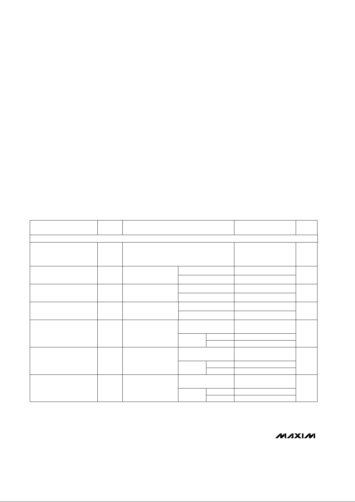
ELECTRICAL CHARACTERISTICS—Single +5V Supply
(V+ = 5V ±10%, GND = 0V, V
INH
= 2.4V, V
INL
= 0.8V, TA= T
MIN
to T
MAX
, unless otherwise noted.)
PARAMETER SYMBOL
MIN TYP MAX
(Note 2)
UNITS
Analog Signal Range
V
COM,
V
NO,
V
NC
0 V+ V
CONDITIONS
(Note 3)
On-Resistance R
ON
33 60
Ω
V+ = 4.5V,
I
COM
= 1.0mA,
VNOor VNC= 3.5V
TA= +25°C
TA= +25°C
TA= +25°C
TA= +25°C
TA= +25°C
TA= +25°C
TA= T
MIN
to T
MAX
TA= T
MIN
to T
MAX
TA= T
MIN
to T
MAX
-40 40
On-Resistance Match
Between Channels (Note 4)
∆R
ON
0.8 2
Ω
V+ = 5V,
I
COM
= 1.0mA,
VNOor VNC= 3V
On-Resistance Flatness
(Notes 3, 5)
R
FLAT(ON)
2 6
Ω
V+ = 5V,
I
COM
= 1.0mA,
VNOor VNC= 1V, 2V, 3V
NO or NC Off Leakage
Current (Note 6)
I
NO(OFF)
or
I
NC(OFF)
-0.1 0.01 0.1
nA
V+ = 5.5V,
V
COM
= 1V,
VNOor VNC= 4.5V
COM Off Leakage Current
(Note 6)
I
COM(OFF)
-0.1 0.1
nA
V+ = 5.5V,
V
COM
= 4.5V,
VNOor VNC= 1V
COM On Leakage Current
(Note 6)
I
COM(ON)
-0.2 0.2
nA
V+ = 5.5V,
V
COM
= 5V, or
V
NO
or VNC= 5V
-5 5
-50 50
75
4
8
-5 5
-40 40
TA= T
MIN
to T
MAX
TA= T
MIN
to T
MAX
TA= T
MIN
to T
MAX
C, E
M
C, E
M
C, E
M
-10 10
ANALOG SWITCH
Note 1: Signals on NC, NO, COM, or IN exceeding V+ or V- are clamped by internal diodes. Limit forward diode current to
maximum current rating.
Page 3
MAX323/MAX324/MAX325
Precision, Single-Supply,
SPST Analog Switches
_______________________________________________________________________________________ 3
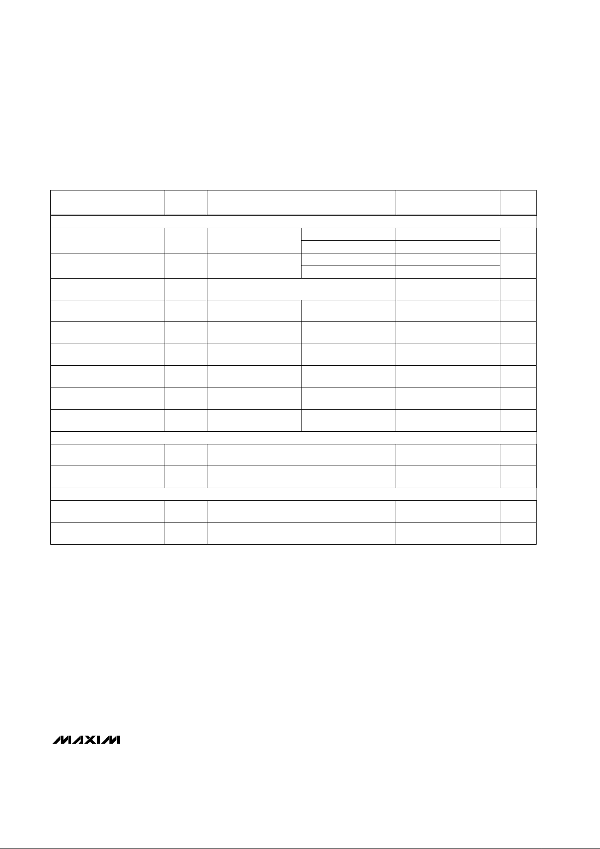
ELECTRICAL CHARACTERISTICS—Single +5V Supply (continued)
(V+ = 5V ±10%, GND = 0V, V
INH
= 2.4V, V
INL
= 0.8V, TA= T
MIN
to T
MAX
, unless otherwise noted.)
PARAMETER SYMBOL
MIN TYP MAX
(Note 2)
UNITSCONDITIONS
Turn-On Time t
ON
85 150
nsVNOor V
NC
= 3V
Break-Before-Make Time
Delay (Note 3)
t
D
2 nsMAX325 only, RL= 300Ω, CL= 35pF
Turn-Off Time t
OFF
25 100
nsVNOor V
NC
= 3V
Power-Supply Range 2.7 16 V
Charge Injection
(Note 3)
Q 1 5 pC
CL= 1.0nF, V
GEN
= 0V,
R
GEN
= 0V, Figure 4
TA= +25°C
TA= +25°C
TA= T
MIN
to T
MAX
TA= T
MIN
to T
MAX
240
150
TA= +25°C
Off Isolation (Note 7) OIRR 72 dB
RL= 50Ω, CL= 5pF,
f = 1MHz, Figure 5
TA= +25°C
Crosstalk (Note 8) 85 dB
RL= 50Ω, CL= 5pF,
f = 1MHz, Figure 6
TA= +25°C
NC or NO Capacitance C
OFF
9 pFf = 1MHz, Figure 7 TA= +25°C
COM Off Capacitance C
COM(OFF)
9 pFf = 1MHz, Figure 7 TA= +25°C
COM On Capacitance C
COM(ON)
22 pFf = 1MHz, Figure 8 TA= +25°C
Input Voltage High V
INH
2.4 V
Input Voltage Low V
INL
0.8 V
Positive Supply Current I+ -1 0.0001 1 µAV+ = 5.5V, VIN= 0V or V+, all channels on or off
DYNAMIC
SUPPLY
LOGIC INPUT
Page 4
MAX323/MAX324/MAX325
Precision, Single-Supply,
SPST Analog Switches
4 _______________________________________________________________________________________
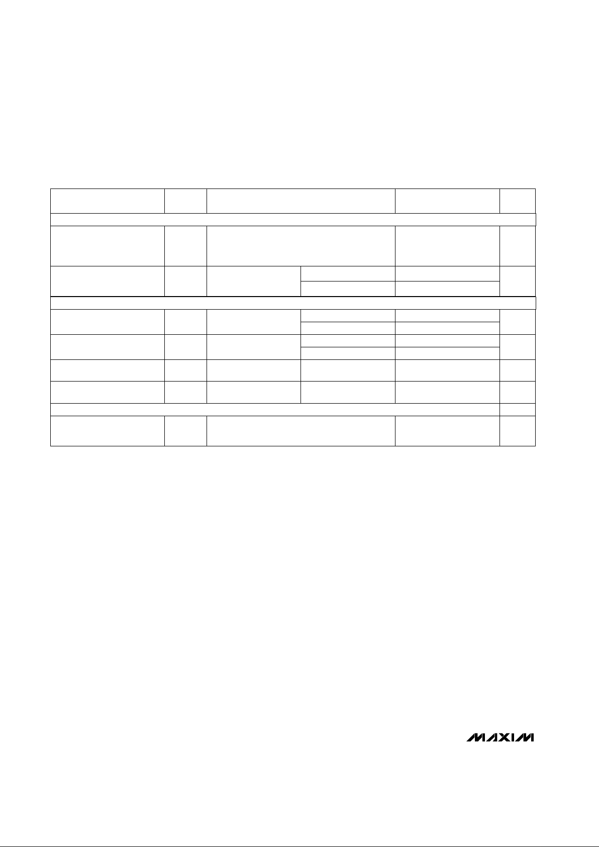
ELECTRICAL CHARACTERISTICS—Single +3.3V Supply
(V+ = 3.0V to 3.6V, GND = 0V, V
INH
= 2.4V, V
INL
= 0.6V, TA= T
MIN
to T
MAX
, unless otherwise noted.)
Note 2: The algebraic convention, where the most negative value is a minimum and the most positive value a maximum, is used in
this data sheet.
Note 3: Guaranteed by design.
Note 4: ∆R
ON
= ∆RONmax - ∆RONmin.
Note 5: Flatness is defined as the difference between the maximum and minimum value of on-resistance as measured over the
specified analog signal range.
Note 6: Leakage parameters are 100% tested at maximum rated hot temperature and guaranteed by correlation at +25°C.
Note 7: Off Isolation = 20 log
10
[ V
COM
⁄ (V
NC or VNO
)
], V
COM
= output, V
NC or VNO
= input to off switch.
Note 8: Between any two switches.
PARAMETER SYMBOL
MIN TYP MAX
(Note 2)
UNITS
Analog Signal Range
V
COM,
V
NO,
V
NC
0 V+ V
CONDITIONS
(Note 3)
Channel On-Resistance R
ON
83 175
Ω
V+ = 3V,
I
COM
= 1.0mA,
VNOor VNC= 1.5V
Turn-On Time (Note 3) t
ON
160 400
nsVNOor VNC= 1.5V
Break-Before-Make Time
Delay (Note 3)
t
D
2 5 ns
MAX325 only,
RL= 300Ω, CL= 35pF
Turn-Off Time (Note 3) t
OFF
40 125
nsVNOor VNC= 1.5V
Positive Supply Current I+ -1 1 µA
Charge Injection (Note 3) Q 1 5 pC
CL= 1.0nF,
V
GEN
= 0V, R
GEN
= 0V
V+ = 3.6V, VIN= 0V or V+, all channels on or off
TA= +25°C
TA= +25°C
TA= +25°C
TA= +25°C
TA= +25°C
TA= T
MIN
to T
MAX
TA= T
MIN
to T
MAX
TA= T
MIN
to T
MAX
275
500
175
ANALOG SWITCH
DYNAMIC
SUPPLY
Page 5

MAX323/MAX324/MAX325
Precision, Single-Supply,
SPST Analog Switches
_______________________________________________________________________________________
5
__________________________________________Typical Operating Characteristics
(TA = +25°C, unless otherwise noted.)
0
0 2 8 10
RON vs. V
COM
60
70
MAX323-01
V
COM
(V)
R
ON
(Ω)
4 6 12
40
10
50
20
30
80
A: V+ = 3V
B: V+ = 5V
C: V+ = 12V
A
B
C
0
0 1 4
RON vs. V
COM
OVER TEMPERATURE
50
MAX323-02
V
COM
(V)
R
ON
(Ω)
2 3 5
30
10
40
20
60
V+ = 5V
A: TA = -55°C
B: T
A
= +25°C
C: T
A
= +85°C
D: T
A
= +125°C
D
C
B
A
0
0 2
∆RON vs. V
COM
OVER TEMPERATURE
MAX323-03
V
COM
(V)
∆R
ON
(Ω)
3 4
0.6
0.2
0.8
0.4
1
5
1
A: TA = -55°C
B: T
A
= +25°C
C: T
A
= +85°C
D: T
A
= +125°C
D
B
C
A
0.0001
ON LEAKAGE CURRENT vs. TEMPERATURE
10
MAX323-04
TEMPERATURE (°C)
ON LEAKAGE (nA)
0.1
0.001
1
0.01
100
-55 65 85-15 5 25 45-35 105 125
0
SUPPLY CURRENT vs. TEMPERATURE
7
8
9
MAX323-07
TEMPERATURE (°C)
I+ (nA)
5
1
2
6
3
4
10
-55 65 85-15 5 25 45-35 105 125
V+ = 5V
IN1, IN2 = GND OR V+
0.0001
OFF LEAKAGE CURRENT vs. TEMPERATURE
10
MAX323-05
TEMPERATURE (°C)
OFF LEAKAGE (nA)
0.1
0.001
1
0.01
100
-55 65 85-15 5 25 45-35 105 125
V+ = 5.5V
V
COM
= 1V
V
NC
OR VNO = 1V
-3
0
CHARGE INJECTION vs. V
COM
2
MAX323-06
V
COM
(V)
Q (pC)
2 5
0
-2
1
-1
3
V+ = 5V
1 3 4
Page 6

MAX323/MAX324/MAX325
Precision, Single-Supply,
SPST Analog Switches
6 _______________________________________________________________________________________
__________Applications Information
Logic Levels
The MAX323/MAX324/MAX325 are TTL compatible
when powered from a single +5V supply. When powered from other supply voltages, TTL compatibility is
not guaranteed, and the logic inputs should be driven
from rail to rail. For example, with a 15V supply, IN1
and IN2 should be driven low to 0V and high to 15V.
Similarly, with a 3.3V supply, IN1 and IN2 should be driven low to 0V and high to 3.3V
Driving IN1 and IN2 rail-to-rail minimizes power consumption.
Analog Signal Levels
Analog signals that range over the entire supply voltage
(V+ to GND) can be switched with very little change in
on-resistance over the entire voltage range (see
Typical
Operating Characteristics
). All the switches are bidirectional, so NO_, NC_, and COM_ pins can be used as
either inputs or outputs.
Power-Supply Sequencing
and Overvoltage Protection
Do not exceed the absolute maximum ratings, because
stresses beyond the listed ratings may cause permanent
damage to the devices.
Proper power-supply sequencing is recommended for
all CMOS devices. Always apply V+ before applying
analog signals or logic inputs, especially if the analog
or logic signals are not current-limited. If this sequencing is not possible, and if the analog or logic inputs are
not current-limited to <30mA, add a small-signal diode
(D1) as shown in Figure 1. If the analog signal can dip
below GND, add D2. Adding protection diodes reduces
the analog signal range to a diode-drop (about 0.7V)
below V+ (for D1), and to a diode-drop above ground
(for D2). Leakage is unaffected by adding the diodes.
On-resistance increases by a small amount at low supply voltages. Maximum supply voltage (V+) must not
exceed 17V.
Adding protection diodes causes the logic thresholds
to be shifted relative to the power-supply rails. This can
be significant when low supply voltages (5V or less) are
used. With a 5V supply, TTL compatibility is not guaranteed when protection diodes are added. Driving IN1
and IN2 all the way to the supply rails (i.e. to a diodedrop higher than the V+ pin, or to a diode-drop lower
than the GND pin) is always acceptable.
Protection diodes D1 and D2 also protect against
some overvoltage situations. With Figure 1’s circuit, if
the supply voltage is below the absolute maximum rating, and if a fault voltage up to the absolute maximum
rating is applied to an analog signal pin, no damage
will result. For example, with a +5V supply, analog signals up to ±8V will not damage the circuit of Figure 1.
If only a single fault signal is present, the fault voltage
can rise to +17V or to -12V without damage occurring.
_____________________Pin Description
POSITIVE SUPPLY
COM
NO
D2
D1
GND
V
g
V+
Figure 1. Overvoltage Protection Using Two External Blocking
Diodes
Normally Closed Analog Switch Terminal
(MAX324/MAX325)
NC2
Normally Open Analog Switch Terminal
(MAX323 only)
NO2
5
GroundGND4
Logic InputsIN2, IN13, 7
PIN
Analog Switch Common Terminal
COM1,
COM2
2, 6
Normally Closed Analog Switch Terminal
(MAX324 only)
NC1
Normally Open Analog Switch Terminal
(MAX323/MAX325)
NO1
1
FUNCTIONNAME
Positive SupplyV+8
Page 7

MAX323/MAX324/MAX325
Precision, Single-Supply,
SPST Analog Switches
_______________________________________________________________________________________ 7
V
GEN
GND
NC
or NO
C
L
V
OUT
V+
V
OUT
IN
OFF
ON
OFF
∆V
OUT
Q = (∆V
OUT
)(CL)
COM
IN DEPENDS ON SWITCH CONFIGURATION;
INPUT POLARITY DETERMINED BY SENSE OF SWITCH.
OFF
ON
OFF
IN
V
IN
= +3V
+5V
R
GEN
IN
MAX323
MAX324
MAX325
Figure 4. Charge Injection
tr < 20ns
tf < 20ns
50%
0V
LOGIC
INPUT
R
L
1kΩ
NO
or NC
GND
C
L
INCLUDES FIXTURE AND STRAY CAPACITANCE.
V
OUT
= V
COM (
R
L
)
RL + R
ON
SWITCH
INPUT
IN
+3V
t
OFF
0V
COM
SWITCH
OUTPUT
0.9 x V
0UT
0.9 x V
OUT
t
ON
V
OUT
SWITCH
OUTPUT
LOGIC
INPUT
LOGIC INPUT WAVEFORMS INVERTED FOR SWITCHES
THAT HAVE THE OPPOSITE LOGIC SENSE.
V+
C
L
35pF
+5V
V
OUT
V
COM
0V
MAX323
MAX324
MAX325
50%
0.9 x V
0UT1
+3V
0V
0V
LOGIC
INPUT
SWITCH
OUTPUT 2
(V
OUT2
)
0V
0.9 x V
OUT2
t
D
t
D
LOGIC
INPUT
R
L2
300Ω
GND
C
L
INCLUDES FIXTURE AND STRAY CAPACITANCE.
COM2
IN
COM1
V
OUT2
V+
+5V
C
L2
35pF
V
COM1
= +3V
R
L1
300Ω
V
OUT1
C
L1
35pF
NO1
NC2
SWITCH
OUTPUT 1
(V
OUT1
)
MAX325
V
COM2
= +3V
Figure 2. Switching Time
Figure 3. Break-Before-Make Interval (MAX325 only)
______________________________________________Test Circuits/Timing Diagrams
Page 8

MAX323/MAX324/MAX325
Precision, Single-Supply,
SPST Analog Switches
8 _______________________________________________________________________________________
Figure 6. Crosstalk
IN
0V or
2.4V
SIGNAL
GENERATOR 0dBm
+5V
10nF
ANALYZER
NC
or NO
R
L
GND
COM
COM
V+
MAX323
MAX324
MAX325
SIGNAL
GENERATOR 0dBm
+5V
10nF
ANALYZER
N02
R
L
GND
COM1
0V or 2.4V
IN1
N01
50Ω
COM2
IN2
0V or
2.4V
NC
V+
MAX323
MAX324
MAX325
Figure 5. Off Isolation
_________________________________Test Circuits/Timing Diagrams (continued)
CAPACITANCE
METER
NC
or NO
COM
GND
IN
0V or
2.4V
10nF
+5V
f = 1MHz
V+
MAX323
MAX324
MAX325
Figure 8. Channel-On Capacitance
CAPACITANCE
METER
NC or
NO
COM
GND
IN
0V or
2.4V
10nF
+5V
f = 1MHz
V+
MAX323
MAX324
MAX325
Figure 7. Channel-Off Capacitance
Page 9

MAX323/MAX324/MAX325
Precision, Single-Supply,
SPST Analog Switches
_______________________________________________________________________________________ 9
__Ordering Information (continued) ___________________Chip Topography
0.075"
(1.90mm)
0.055"
(1.40mm)
V+
IN2
V-
IN1
COM2
NO/NC
COM1
NO/NC
* Contact factory for dice specifications.
** Contact factory for availability.
TRANSISTOR COUNT: 91
SUBSTRATE IS CONNECTED TO V+
8 CERDIP**-55°C to +125°CMAX324MJA
8 CERDIP**-40°C to +85°CMAX324EJA
8 SO-40°C to +85°CMAX324ESA
8 SO0°C to +70°CMAX324CSA
8 µMAX0°C to +70°CMAX324CUA
8 Plastic DIP0°C to +70°C
MAX324CPA
PIN-PACKAGETEMP. RANGEPART
8 Plastic DIP-40°C to +85°CMAX324EPA
Dice*0°C to +70°CMAX324C/D
8 CERDIP**-55°C to +125°CMAX325MJA
8 CERDIP**-40°C to +85°CMAX325EJA
8 SO-40°C to +85°CMAX325ESA
8 SO0°C to +70°CMAX325CSA
8 µMAX0°C to +70°CMAX325CUA
8 Plastic DIP-40°C to +85°CMAX325EPA
8 Plastic DIP0°C to +70°C
MAX325CPA
Dice*0°C to +70°CMAX325C/D
Page 10

MAX323/MAX324/MAX325
Precision, Single-Supply,
SPST Analog Switches
10 ______________________________________________________________________________________
________________________________________________________Package Information
L
α
C
A1B
DIM
A
A1
B
C
D
E
e
H
L
α
MIN
0.036
0.004
0.010
0.005
0.116
0.116
0.188
0.016
0°
MAX
0.044
0.008
0.014
0.007
0.120
0.120
0.198
0.026
6°
MIN
0.91
0.10
0.25
0.13
2.95
2.95
4.78
0.41
0°
MAX
1.11
0.20
0.36
0.18
3.05
3.05
5.03
0.66
6°
INCHES MILLIMETERS
8-PIN µMAX
MICROMAX SMALL OUTLINE
PACKAGE
0.650.0256
A
e
E H
D
0.101mm
0.004 in
DIM
A
A1
A2
A3
B
B1
C
D1
E
E1
e
eA
eB
L
MIN
–
0.015
0.125
0.055
0.016
0.045
0.008
0.005
0.300
0.240
0.100
0.300
–
0.115
MAX
0.200
–
0.175
0.080
0.022
0.065
0.012
0.080
0.325
0.310
–
–
0.400
0.150
MIN
–
0.38
3.18
1.40
0.41
1.14
0.20
0.13
7.62
6.10
2.54
7.62
–
2.92
MAX
5.08
–
4.45
2.03
0.56
1.65
0.30
2.03
8.26
7.87
–
–
10.16
3.81
INCHES MILLIMETERS
Plastic DIP
PLASTIC
DUAL-IN-LINE
PACKAGE
(0.300 in.)
DIM
D
D
D
D
D
D
MIN
0.348
0.735
0.745
0.885
1.015
1.14
MAX
0.390
0.765
0.765
0.915
1.045
1.265
MIN
8.84
18.67
18.92
22.48
25.78
28.96
MAX
9.91
19.43
19.43
23.24
26.54
32.13
INCHES MILLIMETERS
PINS
8
14
16
18
20
24
C
A
A2
E1
D
E
eA
eB
A3
B1
B
0° - 15°
A1
L
D1
e
Page 11

MAX323/MAX324/MAX325
Precision, Single-Supply,
SPST Analog Switches
______________________________________________________________________________________ 11
___________________________________________Package Information (continued)
DIM
A
A1
B
C
E
e
H
L
MIN
0.053
0.004
0.014
0.007
0.150
0.228
0.016
MAX
0.069
0.010
0.019
0.010
0.157
0.244
0.050
MIN
1.35
0.10
0.35
0.19
3.80
5.80
0.40
MAX
1.75
0.25
0.49
0.25
4.00
6.20
1.27
INCHES MILLIMETERS
21-0041A
SO
SMALL OUTLINE
PACKAGE
(0.150 in.)
DIM
D
D
D
MIN
0.189
0.337
0.386
MAX
0.197
0.344
0.394
MIN
4.80
8.55
9.80
MAX
5.00
8.75
10.00
INCHES MILLIMETERS
PINS
8
14
16
1.270.050
L
0°-8°
HE
D
e
A
A1
C
0.101mm
0.004in.
B
Page 12

MAX323/MAX324/MAX325
Precision, Single-Supply,
SPST Analog Switches
Maxim cannot assume responsibility for use of any circuitry other than circuitry entirely embodied in a Maxim product. No circuit patent licenses are
implied. Maxim reserves the right to change the circuitry and specifications without notice at any time.
12
____________________Maxim Integrated Products, 120 San Gabriel Drive, Sunnyvale, CA 94086 408-737-7600
© 1997 Maxim Integrated Products Printed USA is a registered trademark of Maxim Integrated Products.
DIM
A
B
B2
C
E
eA
e
L
Q
S1
MIN
–
0.014
0.038
0.008
0.220
0.290
0.125
0.015
0.005
MAX
0.225
0.023
0.065
0.015
0.310
0.320
0.200
0.070
–
MIN
–
0.36
0.97
0.20
5.59
7.37
3.18
0.38
0.13
MAX
5.72
0.58
1.65
0.38
7.87
8.13
5.08
1.78
–
INCHES MILLIMETERS
Ceramic SB
CERAMIC SIDEBRAZE
PACKAGE
(0.300 in.)
DIM
D
D
D
D
D
D
MIN
–
–
–
–
–
–
MAX
0.550
0.785
0.840
0.960
1.060
1.280
MIN
–
–
–
–
–
–
MAX
13.97
19.94
21.34
24.38
26.92
32.51
INCHES MILLIMETERS
PINS
8
14
16
18
20
24
2.54
C
L
0°-15°
D
E
eA
A
B2
B
e
Q
S1
0.100
___________________________________________Package Information (continued)
 Loading...