

Page 1
MAX3243
3-V TO 5.5-V MULTICHANNEL RS-232 LINE DRIVER/RECEIVER
SLLS350B – APRIL 1999 – REVISED JANUARY 2000
D
Single-Chip and Single-Supply Interface for
IBM PC/AT Serial Port
D
Meets or Exceeds the Requirements of
TIA/EIA-232-F and ITU v.28 Standards
D
Operates With 3-V to 5.5-V VCC Supply
D
Always-Active Noninverting Receiver
Output (ROUT2B)
D
Operates up to 250 kbit/s
D
Low Standby Current ...1 µA Typical
D
External Capacitors ...4 × 0.1 µF
D
Accepts 5-V Logic Input With 3.3-V Supply
D
Designed to Be Interchangeable With
Maxim MAX3243
D
Serial-Mouse Driveability
D
RS-232 Bus-Pin ESD Protection Exceeds
±15-kV Using Human-Body Model (HBM)
D
Applications
– Battery-Powered Systems, PDAs,
Notebooks, Laptops, Palmtop PCs, and
Hand-Held Equipment
D
Package Options Include Plastic
Small-Outline (DW), Shrink Small-Outline
(DB), and Thin Shrink Small-Outline (PW)
Packages
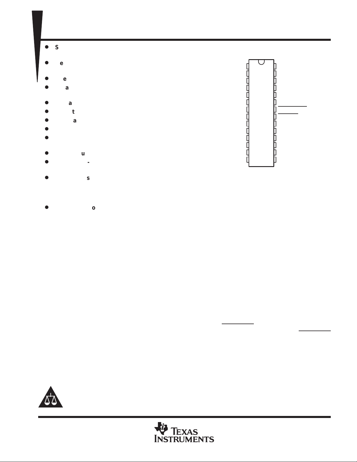
DB, DW, OR PW PACKAGE
(TOP VIEW)
C2+
C2–
V–
RIN1
RIN2
RIN3
RIN4
RIN5
DOUT1
DOUT2
DOUT3
DIN3
DIN2
DIN1
1
2
3
4
5
6
7
8
9
10
11
12
13
14
C1+
28
V+
27
V
26
GND
25
C1–
24
FORCEON
23
FORCEOFF
22
INVALID
21
ROUT2B
20
ROUT1
19
ROUT2
18
ROUT3
17
16
ROUT4
15
ROUT5
CC
description
The MAX3243 device consists of three line drivers, five line receivers, and a dual charge-pump circuit with
±15-kV ESD protection pin-to-pin (serial-port connection pins, including GND). The device meets the
requirements of TIA/EIA-232-F and provides the electrical interface between an asynchronous communication
controller and the serial-port connector. This combination of drivers and receivers matches that needed for the
typical serial port used in an IBM PC/AT, or compatible. The charge pump and four small external capacitors
allow operation from a single 3-V to 5.5-V supply . In addition, the device includes an always-active noninverting
output (ROUT2B), which allows applications using the ring indicator to transmit data while the device is powered
down. The device operates at data signaling rates up to 250 kbit/s and a maximum of 30-V/µs driver output slew
rate.
Flexible control options for power management are available when the serial port is inactive. The
auto-powerdown feature functions when FORCEON is low and FORCEOFF
operation, if the device does not sense a valid RS-232 signal, the driver outputs are disabled. If FORCEOFF
is set low, both drivers and receivers (except ROUT2B) are shut of f, and the supply current is reduced to 1 µA.
Disconnecting the serial port or turning off the peripheral drivers causes the auto-powerdown condition to occur .
Please be aware that an important notice concerning availability, standard warranty, and use in critical applications of
Texas Instruments semiconductor products and disclaimers thereto appears at the end of this data sheet.
is high. During this mode of
PRODUCT PREVIEW
AT, IBM, and PC are trademarks of International Business Machines Corporation.
PRODUCT PREVIEW information concerns products in the formative or
design phase of development. Characteristic data and other
specifications are design goals. Texas Instruments reserves the right to
change or discontinue these products without notice.
POST OFFICE BOX 655303 • DALLAS, TEXAS 75265
Copyright 2000, Texas Instruments Incorporated
1
Page 2
MAX3243
OUTPUT
y
Normal o eration with
3-V TO 5.5-V MULTICHANNEL RS-232 LINE DRIVER/RECEIVER
SLLS350B – APRIL 1999 – REVISED JANUARY 2000
description (continued)
Auto-powerdown can be disabled when FORCEON and FORCEOFF are high, and should be done when driving
a serial mouse. With auto-powerdown enabled, the device is activated automatically when a valid signal is
applied to any receiver input. The INV ALID output is used to notify the user if an RS-232 signal is present at any
receiver input. INV ALID
or has been between –0.3 V and 0.3 V for less than 30 µs. INVALID is low (invalid data) if all receiver input
voltages are between –0.3 V and 0.3 V for more than 30 µs. Refer to Figure 5 for receiver input levels.
The MAX3243C is characterized for operation from 0°C to 70°C. The MAX3243I is characterized for operation
from –40°C to 85°C.
is high (valid data) if any receiver input voltage is greater than 2.7 V or less than –2.7 V
AVAILABLE OPTIONS
PACKAGED DEVICES
T
A
0°C to 70°C MAX3243CDB MAX3243CDW MAX3243CPW
–40°C to 85°C MAX3243IDB MAX3243IDW MAX3243IPW
The DB, DW, and PW packages are available taped and reeled. Add the suffix R to
device type (e.g., MAX3243CDBR).
SHRINK
SMALL OUTLINE
(DB)
SMALL OUTLINE
(DW)
THIN SHRINK
SMALL OUTLINE
(PW)
DIN FORCEON
X X L X Z Powered off
L H H X H
H HH XL
L L H Yes H
H LHYesL
PRODUCT PREVIEW
L L H No Z
H L H No Z
H = high level, L = low level, X = irrelevant, Z = high impedance
INPUTS
RIN2
L X L X L Z
H XL XH Z
L L H Yes L H
L HH YesL L
H LHYesH H
H HHYesH L
Open Open H No L H
H = high level, L = low level, X = irrelevant, Z = high impedance (off), Open = input disconnected or connected
driver off
RIN1,
RIN3–RIN5
INPUTS
FORCEOFF
FORCEOFF
Function Tables
EACH DRIVER
VALID RIN
RS-232 LEVEL
EACH RECEIVER
VALID RIN
RS-232 LEVEL
DOUT
auto-powerdown disabled
auto-powerdown enabled
auto-powerdown feature
OUTPUTS
ROUT2B ROUT
DRIVER STATUS
Normal operation with
Normal operation with
Powered off by
RECEIVER STATUS
Powered off while
ROUT2B is active
p
auto-powerdown
disabled/enabled
2
POST OFFICE BOX 655303 • DALLAS, TEXAS 75265
Page 3
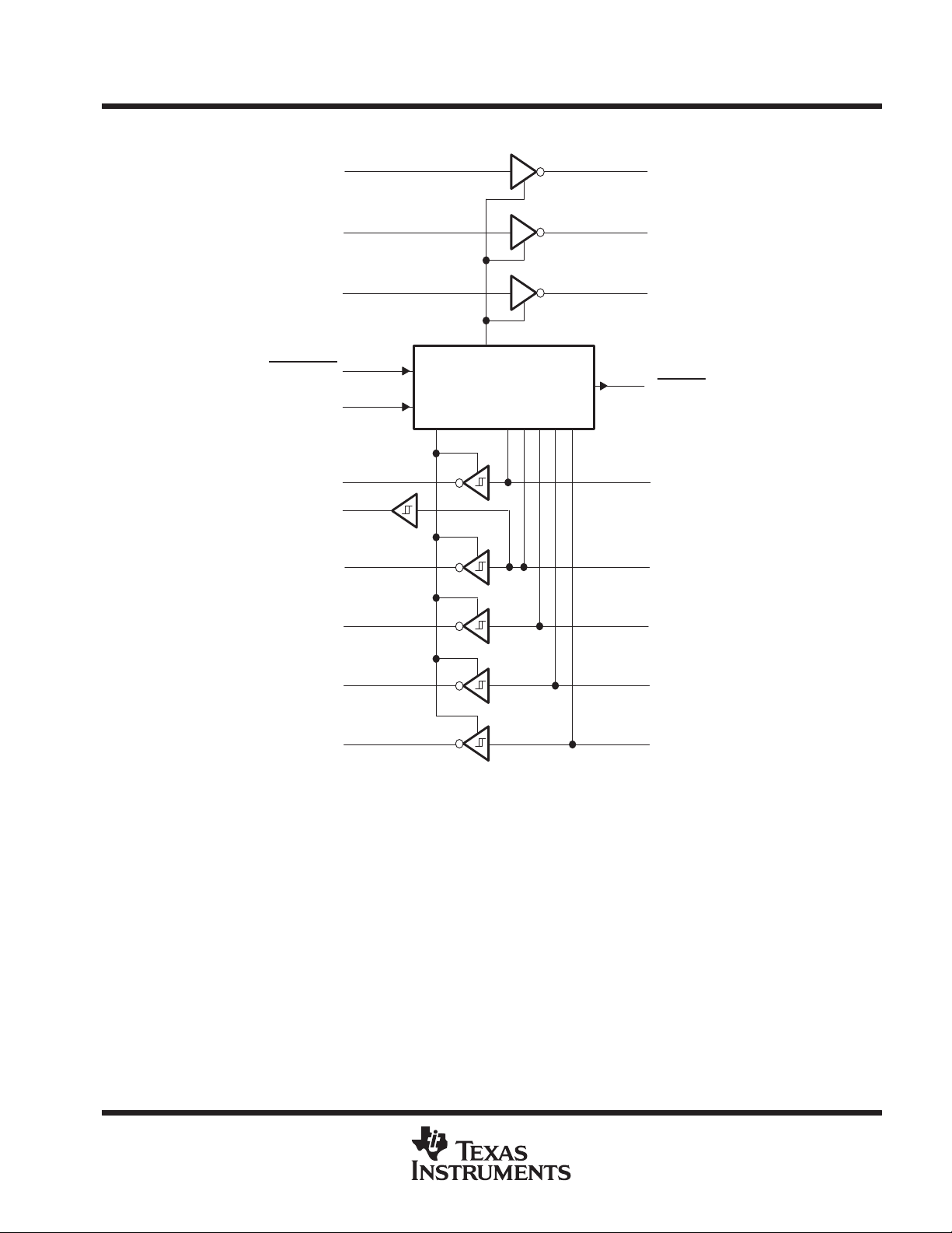
logic diagram (positive logic)
MAX3243
3-V TO 5.5-V MULTICHANNEL RS-232 LINE DRIVER/RECEIVER
SLLS350B – APRIL 1999 – REVISED JANUARY 2000
DIN1
DIN2
DIN3
FORCEOFF
FORCEON
ROUT1
ROUT2B
ROUT2
14
13
12
22
23
19
20
18
Auto-powerdown
10
11
21
9
4
5
DOUT1
DOUT2
DOUT3
INVALID
RIN1
RIN2
ROUT3
ROUT4
ROUT5
17
16
15
6
RIN3
7
RIN4
8
RIN5
PRODUCT PREVIEW
POST OFFICE BOX 655303 • DALLAS, TEXAS 75265
3
Page 4
MAX3243
Suppl
oltage
V
VIHDriver and control high-level input voltage
DIN, FORCEOFF, FORCEON
V
TAO erating free-air tem erature
°C
ICCSu ly current
3-V TO 5.5-V MULTICHANNEL RS-232 LINE DRIVER/RECEIVER
SLLS350B – APRIL 1999 – REVISED JANUARY 2000
absolute maximum ratings over operating free-air temperature range (unless otherwise noted)
Supply voltage range, VCC (see Note 1) –0.3 V to 6 V. . . . . . . . . . . . . . . . . . . . . . . . . . . . . . . . . . . . . . . . . . . . . .
Positive output supply voltage range, V+ (see Note 1) –0.3 V to 7 V. . . . . . . . . . . . . . . . . . . . . . . . . . . . . . . . . .
Negative output supply voltage range, V– (see Note 1) 0.3 V to –7 V. . . . . . . . . . . . . . . . . . . . . . . . . . . . . . . . .
Supply voltage difference, V+
– V– (see Note 1) 13 V. . . . . . . . . . . . . . . . . . . . . . . . . . . . . . . . . . . . . . . . . . . . . . .
Input voltage range, VI: Driver (FORCEOFF, FORCEON) –0.3 V to 6 V. . . . . . . . . . . . . . . . . . . . . . . . . . . . . . .
Receiver –25 V to 25 V. . . . . . . . . . . . . . . . . . . . . . . . . . . . . . . . . . . . . . . . . . . . . . . . . . . .
Output voltage range, VO: Driver –13.2 V to 13.2 V. . . . . . . . . . . . . . . . . . . . . . . . . . . . . . . . . . . . . . . . . . . . . . . . .
Receiver (INVALID) –0.3 V to VCC + 0.3 V. . . . . . . . . . . . . . . . . . . . . . . . . . . . . . . . .
Package thermal impedance, θJA (see Note 2): DB package 62°C/W. . . . . . . . . . . . . . . . . . . . . . . . . . . . . . . . .
DW package 46°C/W. . . . . . . . . . . . . . . . . . . . . . . . . . . . . . . . .
PW package 62°C/W. . . . . . . . . . . . . . . . . . . . . . . . . . . . . . . . .
Lead temperature 1,6 mm (1/16 inch) from case for 10 seconds 260°C. . . . . . . . . . . . . . . . . . . . . . . . . . . . . . .
Storage temperature range, T
†
Stresses beyond those listed under “absolute maximum ratings” may cause permanent damage to the device. These are stress ratings only, and
functional operation of the device at these or any other conditions beyond those indicated under “recommended operating conditions” is not
implied. Exposure to absolute-maximum-rated conditions for extended periods may affect device reliability.
NOTES: 1. All voltages are with respect to network GND.
2. The package thermal impedance is calculated in accordance with JESD 51.
–65°C to 150°C. . . . . . . . . . . . . . . . . . . . . . . . . . . . . . . . . . . . . . . . . . . . . . . . . . .
stg
recommended operating conditions (see Note 3 and Figure 6)
MIN NOM MAX UNIT
pp
y v
p
V
V
V
PRODUCT PREVIEW
NOTE 3: Test conditions are C1–C4 = 0.1 µF at VCC = 3.3 V ± 0.3 V; C1 = 0.047 µF, C2–C4 = 0.33 µF at VCC = 5 V ± 0.5 V.
Driver and control low-level input voltage DIN, FORCEOFF, FORCEON 0.8 V
IL
Driver and control input voltage DIN, FORCEOFF, FORCEON 0 5.5 V
I
Receiver input voltage –25 25 V
I
p
p
VCC = 3.3 V 3 3.3 3.6
VCC = 5 V 4.5 5 5.5
VCC = 3.3 V 2
VCC = 5 V 2.4
MAX3243C 0 70
MAX3243I –40 85
†
°
electrical characteristics over recommended ranges of supply voltage and operating free-air
temperature (unless otherwise noted) (see Note 3 and Figure 6)
PARAMETER TEST CONDITIONS MIN TYP‡MAX UNIT
I
Input leakage current FORCEOFF, FORCEON ±0.01 ±1 µA
I
pp
‡
All typical values are at VCC = 3.3 V or VCC = 5 V, and TA = 25°C.
NOTE 3. Test conditions are C1–C4 = 0.1 µF at VCC = 3.3 V ± 0.3 V; C1 = 0.047 µF, C2–C4 = 0.33 µF at VCC = 5 V ± 0.5 V.
4
Auto-powerdown disabled
Powered off No load, FORCEOFF at GND 1 10
Auto-powerdown enabled
POST OFFICE BOX 655303 • DALLAS, TEXAS 75265
No load,
FORCEOFF
No load, FORCEOFF at VCC,
FORCEON at GND,
All RIN are open or grounded
and FORCEON at V
CC
0.3 1 mA
1 10
µA
Page 5

MAX3243
I
Sh
‡
±35
±60
mA
SR(tr)
g
CC
V/µs
3-V TO 5.5-V MULTICHANNEL RS-232 LINE DRIVER/RECEIVER
SLLS350B – APRIL 1999 – REVISED JANUARY 2000
DRIVER SECTION
electrical characteristics over recommended ranges of supply voltage and operating free-air
temperature (unless otherwise noted) (see Note 3 and Figure 6)
PARAMETER TEST CONDITIONS MIN TYP†MAX UNIT
V
V
V
I
IH
I
IL
OS
r
o
I
off
†
All typical values are at VCC = 3.3 V or VCC = 5 V, and TA = 25°C.
‡
Short-circuit durations should be controlled to prevent exceeding the device absolute power dissipation ratings, and not more than one output
should be shorted at a time.
NOTE 3. Test conditions are C1–C4 = 0.1 µF at VCC = 3.3 V ± 0.3 V; C1 = 0.047 µF, C2–C4 = 0.33 µF at VCC = 5 V ± 0.5 V.
High-level output voltage All DOUT at RL = 3 kΩ to GND 5 5.4 V
OH
Low-level output voltage All DOUT at RL = 3 kΩ to GND –5 –5.4 V
OL
Output voltage
O
(mouse driveability)
High-level input current VI = V
Low-level input current VI at GND ±0.01 ±1 µA
ort-circuit output current
Output resistance VCC, V+, and V– = 0 V, VO = ±2 V 300 10M Ω
Output leakage current FORCEOFF = GND, VO = ±12 V, VCC = 0 to 5.5 V ±25 µA
DIN1 = DIN2 = GND, DIN3 = VCC,
3-kΩ to GND at DOUT3,
DOUT1 = DOUT2 = 2.5 mA
CC
VCC = 3.6 V, VO = 0 V
VCC = 5.5 V, VO = 0 V
±5 V
±0.01 ±1 µA
switching characteristics over recommended ranges of supply voltage and operating free-air
temperature (unless otherwise noted) (see Note 3 and Figure 6)
PARAMETER TEST CONDITIONS MIN TYP†MAX UNIT
Maximum data rate
t
sk(p)
†
All typical values are at VCC = 3.3 V or VCC = 5 V, and TA = 25°C.
§
Pulse skew is defined as |t
NOTE 3. Test conditions are C1–C4 = 0.1 µF at VCC = 3.3 V ± 0.3 V; C1 = 0.047 µF, C2–C4 = 0.33 µF at VCC = 5 V ± 0.5 V.
Pulse skew
Slew rate, transition region VCC = 3.3 V,
(see Figure 1)
§
– t
PLH
PHL
CL = 1000 pF,
One DOUT switching,
CL = 150 pF to 2500 pF
RL = 3 kΩ to 7 kΩ
| of each channel of the same device.
RL = 3 kΩ,
See Figure 1
RL = 3 kΩ to 7 kΩ,
See Figure 2
CL = 150 pF to 1000 pF 6 30
CL = 150 pF to 2500 pF 4 30
250 kbit/s
100 ns
PRODUCT PREVIEW
POST OFFICE BOX 655303 • DALLAS, TEXAS 75265
5
Page 6

MAX3243
V
Positive-going input threshold voltage
V
V
Negative-going input threshold voltage
V
C
150 pF, See Figure 3
C
150 pF, R
See Figure 4
3-V TO 5.5-V MULTICHANNEL RS-232 LINE DRIVER/RECEIVER
SLLS350B – APRIL 1999 – REVISED JANUARY 2000
RECEIVER SECTION
electrical characteristics over recommended ranges of supply voltage and operating free-air
temperature (unless otherwise noted) (see Note 3 and Figure 6)
PARAMETER TEST CONDITIONS MIN TYP
V
V
V
I
off
r
i
†
All typical values are at VCC = 3.3 V or VCC = 5 V, and TA = 25°C.
NOTE 3. Test conditions are C1–C4 = 0.1 µF at VCC = 3.3 V ± 0.3 V; C1 = 0.047 µF, C2–C4 = 0.33 µF at VCC = 5 V ± 0.5 V.
High-level output voltage IOH = –1 mA VCC – 0.6 V VCC – 0.1 V V
OH
Low-level output voltage IOL = 1.6 mA 0.4 V
OL
IT+
IT–
Input hysteresis (V
hys
Output leakage current (except ROUT2B) FORCEOFF = 0 V ±0.05 ±10 µA
Input resistance VI = ±3 V to ±25 V 3 5 7 kΩ
p
p
– V
IT+
) 0.5 V
IT–
VCC = 3.3 V 1.6 2.4
VCC = 5 V 1.9 2.4
VCC = 3.3 V 0.6 1.1
VCC = 5 V 0.8 1.4
switching characteristics over recommended ranges of supply voltage and operating free-air
temperature (unless otherwise noted) (see Note 3)
PARAMETER TEST CONDITIONS MIN TYP†MAX UNIT
t
PLH
t
PHL
t
en
t
dis
t
sk(p)
†
All typical values are at VCC = 3.3 V or VCC = 5 V, and TA = 25°C.
‡
Pulse skew is defined as |t
NOTE 3. Test conditions are C1–C4 = 0.1 µF at VCC = 3.3 V ± 0.3 V; C1 = 0.047 µF, C2–C4 = 0.33 µF at VCC = 5 V ± 0.5 V.
Propagation delay time, low- to high-level output
Propagation delay time, high- to low-level output
Output enable time
Output disable time
Pulse skew
‡
– t
PLH
| of each channel of the same device.
PHL
p
=
L
p
=
L
See Figure 3 50 ns
= 3 kΩ,
L
†
MAX UNIT
150 ns
150 ns
200 ns
200 ns
PRODUCT PREVIEW
6
POST OFFICE BOX 655303 • DALLAS, TEXAS 75265
Page 7

MAX3243
3-V TO 5.5-V MULTICHANNEL RS-232 LINE DRIVER/RECEIVER
SLLS350B – APRIL 1999 – REVISED JANUARY 2000
AUTO-POWERDOWN SECTION
electrical characteristics over recommended ranges of supply voltage and operating free-air
temperature (unless otherwise noted) (see Figure 5)
PARAMETER TEST CONDITIONS MIN
V
T+(valid)
V
T–(valid)
V
T(invalid)
V
OH
V
OL
†
All typical values are at VCC = 3.3 V or VCC = 5 V, and TA = 25°C.
Receiver input threshold
for INVALID
Receiver input threshold
for INVALID
Receiver input threshold
for INVALID
INVALID high-level output voltage
INVALID low-level output voltage
high-level output voltage
high-level output voltage
low-level output voltage
FORCEON = GND,
FORCEOFF
FORCEON = GND,
FORCEOFF
FORCEON = GND,
FORCEOFF
IOH = –1 mA, FORCEON = GND,
FORCEOFF
IOL = 1.6 mA, FORCEON = GND,
FORCEOFF
= V
= V
= V
= V
= V
CC
CC
CC
CC
CC
–2.7 V
–0.3 0.3 V
VCC – 0.6 V
switching characteristics over recommended ranges of supply voltage and operating free-air
temperature (unless otherwise noted) (see Figure 5)
PARAMETER MIN TYP†MAX UNIT
t
valid
t
invalid
t
en
†
All typical values are at VCC = 3.3 V or VCC = 5 V, and TA = 25°C.
Propagation delay time, low- to high-level output 1 µs
Propagation delay time, high- to low-level output 30 µs
Supply enable time 100 µs
TYP
†
MAX UNIT
2.7 V
0.4 V
PARAMETER MEASUREMENT INFORMATION
Generator
(see Note B)
NOTES: A. CL includes probe and jig capacitance.
B. The pulse generator has the following characteristics: PRR = 250 kbit/s, ZO = 50 Ω, 50% duty cycle, tr ≤10 ns, tf ≤ 10 ns.
50 Ω
R
L
3 V
FORCEOFF
TEST CIRCUIT VOLTAGE WAVEFORMS
6V
or t
Input
Output
TLH
RS-232
Output
CL
(see Note A)
SR(tr)
+
t
THL
Figure 1. Driver Slew Rate
t
THL
3 V
–3 V
–3 V
3 V
t
TLH
3 V
0 V
V
V
PRODUCT PREVIEW
OH
OL
POST OFFICE BOX 655303 • DALLAS, TEXAS 75265
7
Page 8

MAX3243
3-V TO 5.5-V MULTICHANNEL RS-232 LINE DRIVER/RECEIVER
SLLS350B – APRIL 1999 – REVISED JANUARY 2000
PARAMETER MEASUREMENT INFORMATION
Input
Output
Generator
(see Note B)
RS-232
Output
50 Ω
R
L
3 V
FORCEOFF
TEST CIRCUIT VOLTAGE WAVEFORMS
CL
(see Note A)
1.5 V
50%
t
PHL
1.5 V
50%
t
PLH
3 V
0 V
V
V
OH
OL
NOTES: A. CL includes probe and jig capacitance.
NOTES: A. CL includes probe and jig capacitance.
B. The pulse generator has the following characteristics: PRR = 250 kbit/s, ZO = 50 Ω, 50% duty cycle, tr ≤ 10 ns, tf ≤ 10 ns.
3 V or 0 V
FORCEON
Generator
(see Note B)
B. The pulse generator has the following characteristics: ZO = 50 Ω, 50% duty cycle, tr ≤ 10 ns, tf ≤ 10 ns.
50 Ω
3 V
FORCEOFF
TEST CIRCUIT VOLTAGE WAVEFORMS
Figure 3. Receiver Propagation Delay Times
PRODUCT PREVIEW
3 V or 0 V
FORCEOFF
Generator
(see Note B)
3 V or 0 V
FORCEON
50 Ω
TEST CIRCUIT VOLTAGE WAVEFORMS
Figure 2. Driver Pulse Skew
Output
CL
(see Note A)
V
CC
S1
C
(see Note A)
GND
R
L
Output
L
Input
t
Output
Input
(S1 at GND)
Output
(S1 at VCC)
Output
PHL
t
PHZ
0.3 V
t
PLZ
0.3 V
1.5 V 1.5 V
50% 50%
1.5 V 1.5 V
t
PLH
t
PZH
(S1 at GND)
50%
t
PZL
(S1 at VCC)
50%
3 V
–3 V
V
OH
V
OL
3 V
–3 V
V
V
OH
OL
NOTES: A. CL includes probe and jig capacitance.
B. The pulse generator has the following characteristics: ZO = 50 Ω, 50% duty cycle, tr ≤ 10 ns, tf ≤ 10 ns.
C. t
D. t
PLZ
PZL
and t
and t
are the same as t
PHZ
are the same as ten.
PZH
Figure 4. Receiver Enable and Disable Times
8
POST OFFICE BOX 655303 • DALLAS, TEXAS 75265
dis
.
Page 9

3-V TO 5.5-V MULTICHANNEL RS-232 LINE DRIVER/RECEIVER
SLLS350B – APRIL 1999 – REVISED JANUARY 2000
PARAMETER MEASUREMENT INFORMATION
MAX3243
Generator
(see Note B)
FORCEOFF
FORCEON
2.7 V
Receiver
Input
ROUT
50 Ω
INVALID
Auto-
powerdown
DIN
TEST CIRCUIT VOLTAGE WAVEFORMS
INVALID
CL = 30 pF
(see Note A)
DOUT
Output
V+
Supply
Voltages
V–
2.7 V
0.3 V
0 V
–0.3 V
–2.7 V
†
Auto-powerdown disables drivers and reduces
supply current to 1 µA.
–2.7 V
t
invalid
50% V
CC
Valid RS-232 Level, INVALID
Indeterminate
If Signal Remains Within This Region
For More Than 30 µs, INVALID
Indeterminate
Valid RS-232 Level, INVALID
50% V
High
Is Low
High
2.7 V
–2.7 V
t
valid
t
en
CC
0.3 V
0.3 V
†
3 V
0 V
0 V
–3 V
V
CC
0 V
≈V+
V
CC
0 V
≈V–
PRODUCT PREVIEW
NOTES: A. CL includes probe and jig capacitance.
B. The pulse generator has the following characteristics: PRR = 5 kbit/s, ZO = 50 Ω, 50% duty cycle, tr ≤ 10 ns, tf ≤ 10 ns.
Figure 5. INVALID Propagation Delay Times and Supply Enabling Time
POST OFFICE BOX 655303 • DALLAS, TEXAS 75265
9
Page 10

MAX3243
3-V TO 5.5-V MULTICHANNEL RS-232 LINE DRIVER/RECEIVER
SLLS350B – APRIL 1999 – REVISED JANUARY 2000
APPLICATION INFORMATION
C4
RS-232 Inputs
RS-232 Outputs
C1+
1
2
3
4
5
6
7
8
9
10
C2+
C2–
V–
V
GND
C1–
Auto-
5 kΩ
+
C2
–
–
+
RIN1
RIN2
RIN3
RIN4
RIN5
DOUT1
DOUT2
28
27
V+
26
CC
25
24
23
22
powerdown
21
20
19
+
–
+
C
BYPASS
= 0.1 µF
–
FORCEON
FORCEOFF
INVALID
ROUT2B
ROUT1
C3
†
+
C1
–
DOUT3
DIN3
PRODUCT PREVIEW
Logic Inputs
†
C3 can be connected to VCC or GND.
NOTE A: Resistor values shown are nominal.
DIN2
DIN1
Figure 6. Typical Operating Circuit and Capacitor Values
11
12
13
14
VCC vs CAPACITOR VALUES
V
CC
3.3 V ± 0.3 V
5 V ± 0.5 V
3 V to 5.5 V
C1 C2, C3, and C4
0.1 µF
0.047 µF
0.1 µF
5 kΩ
5 kΩ
5 kΩ
5 kΩ
0.1 µF
0.33 µF
0.47 µF
18
17
16
15
ROUT2
Logic Outputs
ROUT3
ROUT4
ROUT5
10
POST OFFICE BOX 655303 • DALLAS, TEXAS 75265
Page 11

IMPORTANT NOTICE
T exas Instruments and its subsidiaries (TI) reserve the right to make changes to their products or to discontinue
any product or service without notice, and advise customers to obtain the latest version of relevant information
to verify, before placing orders, that information being relied on is current and complete. All products are sold
subject to the terms and conditions of sale supplied at the time of order acknowledgement, including those
pertaining to warranty, patent infringement, and limitation of liability.
TI warrants performance of its semiconductor products to the specifications applicable at the time of sale in
accordance with TI’s standard warranty. Testing and other quality control techniques are utilized to the extent
TI deems necessary to support this warranty . Specific testing of all parameters of each device is not necessarily
performed, except those mandated by government requirements.
CERTAIN APPLICA TIONS USING SEMICONDUCT OR PRODUCTS MAY INVOLVE POTENTIAL RISKS OF
DEATH, PERSONAL INJURY, OR SEVERE PROPERTY OR ENVIRONMENTAL DAMAGE (“CRITICAL
APPLICATIONS”). TI SEMICONDUCTOR PRODUCTS ARE NOT DESIGNED, AUTHORIZED, OR
WARRANTED TO BE SUITABLE FOR USE IN LIFE-SUPPORT DEVICES OR SYSTEMS OR OTHER
CRITICAL APPLICA TIONS. INCLUSION OF TI PRODUCTS IN SUCH APPLICATIONS IS UNDERST OOD TO
BE FULLY AT THE CUSTOMER’S RISK.
In order to minimize risks associated with the customer’s applications, adequate design and operating
safeguards must be provided by the customer to minimize inherent or procedural hazards.
TI assumes no liability for applications assistance or customer product design. TI does not warrant or represent
that any license, either express or implied, is granted under any patent right, copyright, mask work right, or other
intellectual property right of TI covering or relating to any combination, machine, or process in which such
semiconductor products or services might be or are used. TI’s publication of information regarding any third
party’s products or services does not constitute TI’s approval, warranty or endorsement thereof.
Copyright 2000, Texas Instruments Incorporated
 Loading...