

Page 1
General Description
Maxim’s MAX312/MAX313/MAX314 analog switches
feature low on-resistance (10Ω max) and 1.5Ω on-resistance matching between channels. These switches conduct equally well in either direction. They offer low
leakage over temperature (2.5nA at +85°C). Low power
consumption and ESD tolerance greater than 2000V per
Method 3015.7 are guaranteed.
The MAX312/MAX313/MAX314 are quad, singlepole/single-throw (SPST) analog switches. The MAX312
is normally closed (NC), and the MAX313 is normally
open (NO). The MAX314 has two NC switches and two
NO switches. All three devices operate from a single
supply of +4.5V to +30V or from dual supplies of ±4.5V
to ±20V.
________________________Applications
Test Equipment
Communication Systems
PBX, PABX Systems
Audio Signal Routing
Avionics
Sample-and-Hold Circuits
Data Acquisition Systems
____________________________Features
♦♦
Pin Compatible with DG411/DG412/DG413
♦♦
Low On-Resistance (6.5Ω typical)
♦♦
Guaranteed R
ON
Match Between Channels (1.5Ω max)
♦♦
Guaranteed R
ON
Flatness over Specified Signal
Range (2Ω max)
♦♦
Guaranteed ESD Protection > 2000V per Method
3015.7
♦♦
Crosstalk > 96dB at 20kHz
♦♦
Single-Supply Operation: +4.5V to +30V
Dual-Supply Operation: ±4.5V to ±20V
♦♦
Rail-to-Rail
®
Signal Handling
MAX312/MAX313/MAX314
10ΩΩ, Quad, SPST, CMOS Analog Switches
________________________________________________________________
Maxim Integrated Products
1
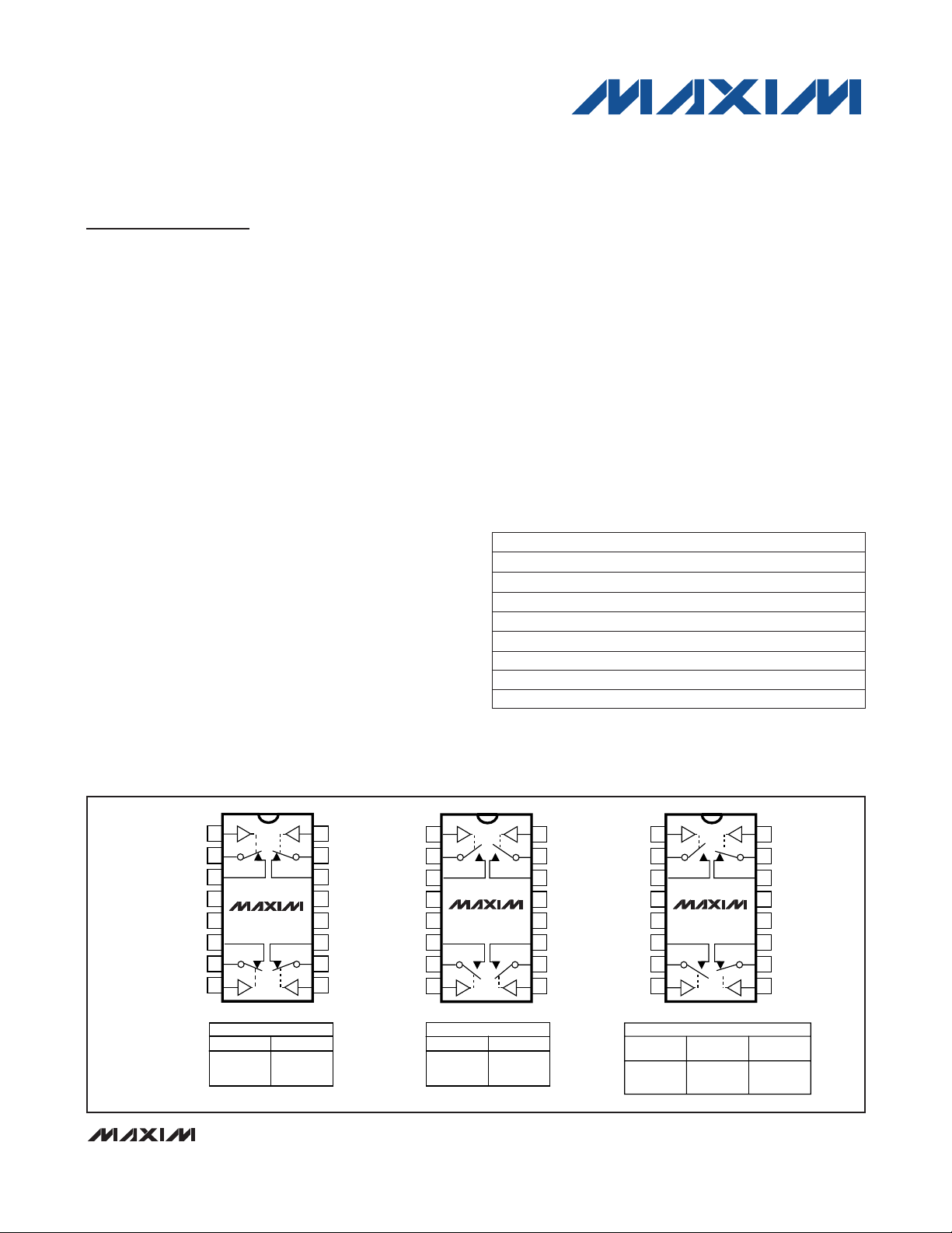
_____________________Pin Configurations/Functional Diagrams/Truth Tables
PART
MAX312CPE
MAX312CSE
MAX312C/D 0°C to +70°C
0°C to +70°C
0°C to +70°C
TEMP RANGE PIN-PACKAGE
16 Plastic DIP
16 Narrow SO
Dice*
19-0420; Rev 2; 7/02
______________Ordering Information
Ordering Information continued at end of data sheet.
* Contact factory for dice specifications.
**Contact factory for availability.
MAX312EPE
MAX312ESE -40°C to +85°C
-40°C to +85°C 16 Plastic DIP
16 Narrow SO
MAX312MJE -55°C to +125°C 16 CERDIP**
MAX312CUE 0°C to +70°C 16 TSSOP
MAX312EUE -40°C to +85°C 16 TSSOP
For pricing, delivery, and ordering information, please contact Maxim/Dallas Direct! at
1-888-629-4642, or visit Maxim’s website at www.maxim-ic.com.
Rail-to-Rail is a registered trademark of Nippon Motorola Ltd.
TOP VIEW
IN1
COM1
NC1
GND
NC4
COM4
IN4
1
2
3
V-
4
5
6
7
8
DIP/SO/TSSOP
SO/MAX312
LOGIC SWITCH
0
1
MAX312
ON
OFF
16
IN2
COM2
15
NC2
14
13
V+
VL
12
11
NC3
10
COM3
9
IN3
1
IN1
2
COM1
3
NO1
V-
4
MAX313
5
GND
6
NO4
7
COM4
8
IN4
DIP/SO/TSSOP
MAX313
LOGIC SWITCH
0
1
SWITCHES SHOWN FOR LOGIC "0" INPUT
OFF
16
IN2
15
COM2
14
NO2
13
V+
12
VL
11
NO3
10
COM3
9
IN3
ON
IN1
COM1
NO1
V-
GND
NO4
COM4
IN4
1
2
3
4
MAX314
5
6
7
8
DIP/SO/TSSOP
MAX314
LOGIC
SWITCHES
1, 4
0
1
OFF
ON
16
15
14
13
12
11
10
9
SWITCHES
2, 3
ON
OFF
IN2
COM2
NC2
V+
VL
NC3
COM3
IN3
Page 2
MAX312/MAX313/MAX314
10ΩΩ, Quad, SPST, CMOS Analog Switches
2 _______________________________________________________________________________________
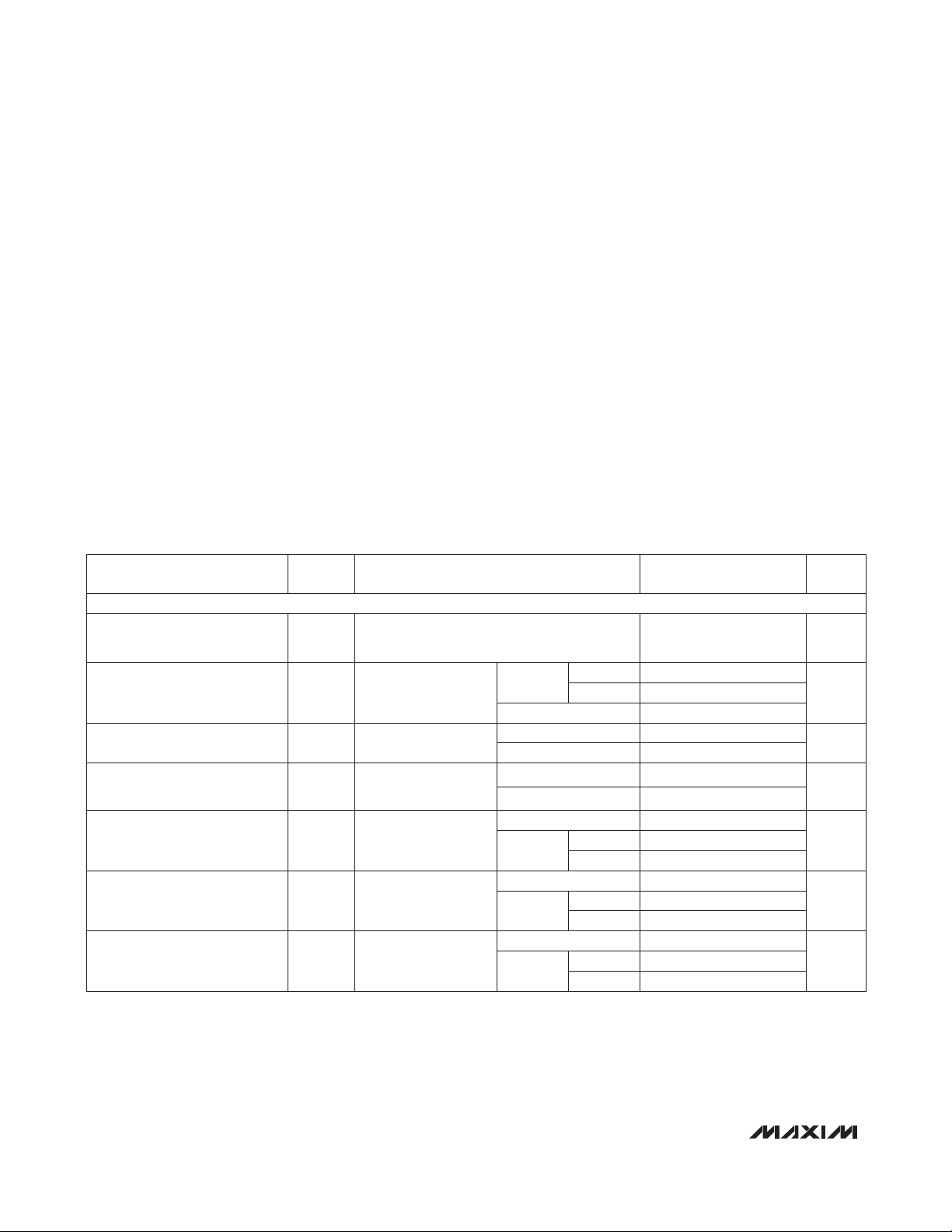
ABSOLUTE MAXIMUM RATINGS
ELECTRICAL CHARACTERISTICS—Dual Supplies
(V+ = 15V, V- = -15V, VL = 5V, GND = 0V, V
INH
= 2.4V, V
INL
= 0.8V, TA= T
MIN
to T
MAX
, unless otherwise noted.)
Stresses beyond those listed under “Absolute Maximum Ratings” may cause permanent damage to the device. These are stress ratings only, and functional
operation of the device at these or any other conditions beyond those indicated in the operational sections of the specifications is not implied. Exposure to
absolute maximum rating conditions for extended periods may affect device reliability.
Voltages Referenced to GND
V+ ...........................................................................-0.3V to +44V
V- ............................................................................+0.3V to -44V
V+ to V-...................................................................-0.3V to +44V
VL .....................................................(GND - 0.3V) to (V+ + 0.3V)
All Other Pins (Note 1) ................................(V- - 2V) to (V+ + 2V)
or 30mA (whichever occurs first)
Continuous Current (COM_, NO_, NC_).........................±100mA
Peak Current (COM_, NO_, NC_) ...................................±300mA
Continuous Power Dissipation (T
A
= +70°C)
Plastic DIP (derate 10.53mW/°C above +70°C) ..........842mW
Narrow SO (derate 8.70mW/°C above +70°C) ............696mW
CERDIP (derate 10.00mW/°C above +70°C)...............800mW
TSSOP (derate 6.7mW/°C above +70°C) ....................457mW
Operating Temperature Ranges
MAX31_C_ ..........................................................0°C to +70°C
MAX31_E_ .......................................................-40°C to +85°C
MAX31_M_.....................................................-55°C to +125°C
Storage Temperature Range .............................-65°C to +150°C
Lead Temperature (soldering, 10s) .................................+300°C
Note 1: Signals on NC_, NO_, COM_, or IN_ exceeding V+ or V- will be clamped by internal diodes. Limit forward diode current to
maximum current rating.
(Note 3)
V
COM
= ±10V,
V
NO
_ or VNC_ = ±10V
I
COM
= 10mA,
V
NO
_ or VNC_ = ±10V
I
COM
= 10mA,
VNO_ or VNC_ = ±10V
CONDITIONS
6.5 10
VV- V+
V
COM
_,
V
NO
_,
VNC_
Analog Signal Range
nA
-40 40
I
NO
I
NC
Off Leakage Current
(NO_ or NC_)
(Note 6)
-2.5 2.5
-0.5 -0.02 0.5
9 Ω
15
R
ON
On-Resistance
0.3 1.5
Ω
3
ΔR
ON
On-Resistance Match Between
Channels (Note 4)
UNITS
MIN TYP MAX
(Note 2)
SYMBOLPARAMETER
C, E
M
TA=
+25°C
TA= T
MIN
to T
MAX
TA= +25°C
TA= T
MIN
to T
MAX
TA= +25°C
TA= T
MIN
to T
MAX
I
COM
= 10mA,
VNO_ or VNC_ = -5V,
0V, 5V
0.2 2
Ω
4
R
FLAT(ON)
On-Resistance Flatness
(Note 5)
TA= +25°C
TA= T
MIN
to T
MAX
C, E
M
V
COM
= ±10V,
VNO_ or VNC_ = ±10V
TA= +25°C
TA= T
MIN
to T
MAX
C, E
M
nA
-40 40
I
NC(OFF)
COM Off Leakage Current
(Note 6)
-2.5 2.5
-0.5 -0.02 0.5
V
COM
= ±10V,
VNO_ or VNC_ = ±10V
TA= +25°C
TA= T
MIN
to T
MAX
C, E
M
nA
-100 100
I
COM(ON)
COM On Leakage Current
(Note 6)
-5 5
-1 -0.04 1
ANALOG SWITCH
Page 3
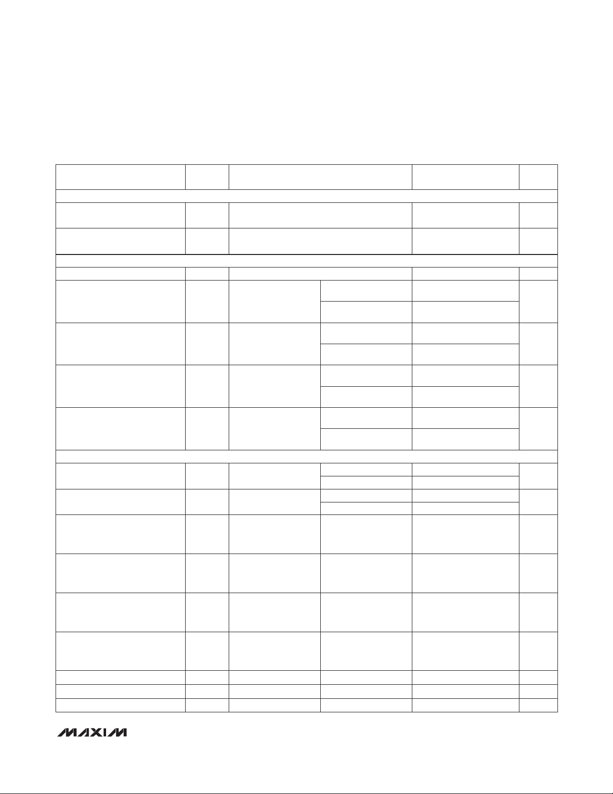
MAX312/MAX313/MAX314
10ΩΩ, Quad, SPST, CMOS Analog Switches
_______________________________________________________________________________________ 3
ELECTRICAL CHARACTERISTICS—Dual Supplies (continued)
(V+ = 15V, V- = -15V, VL = 5V, GND = 0V, V
INH
= 2.4V, V
INL
= 0.8V, TA= T
MIN
to T
MAX
, unless otherwise noted.)
IN_ = 2.4V, all others = 0.8V
CONDITIONS
-1 0.0001 1
µA-0.500 0.005 0.500I
INH
Input Current with Input Voltage
High
-5 5
µAI+
UNITS
MIN TYP MAX
(Note 2)
SYMBOLPARAMETER
TA= +25°C
TA= T
MIN
to T
MAX
IN_ = 0.8V, all others = 2.4V µA-0.500 0.005 0.500I
INL
Input Current with Input Voltage
Low
V±4.5 ±20.0Power-Supply Range
Positive Supply Current
All channels on or off,
V
IN
= 0V or 5V,
V+ = 16.5V
V- = -16.5V
All channels on or off,
V
IN
= 0V or 5V,
V+ = 16.5V
V- = -16.5V
Negative Supply Current
-1 0.0001 1
-5 5
µAI-
TA= +25°C
TA= T
MIN
to T
MAX
All channels on or off,
VIN= 0V or 5V,
V+ = 16.5V
V- = -16.5V
Ground Current
-1 -0.0001 1
-5 5
µAI
GND
TA= +25°C
TA= T
MIN
to T
MAX
All channels on or off,
VIN= 0V or 5V,
V+ = 16.5V
V- = -16.5V
Logic Supply Current
-1 0.0001 1
-5 5
µAI
L
TA= +25°C
TA= T
MIN
to T
MAX
70 225TA= +25°C
MAX314 only, Figure 3,
R
L
= 300Ω,
CL= 35pF
t
D
Break-Before-Make Time Delay ns
Figure 2,
V
COM
= ±10V
15TA= +25°C
t
ON
Turn-On Time ns
275TA= T
MIN
to T
MAX
65 185TA= +25°C
Figure 2,
V
COM
= ±10V
t
OFF
Turn-Off Time ns
235TA= T
MIN
to T
MAX
RL= 50Ω,
CL= 5pF,
f = 1MHz, Figure 6
V
CT
Crosstalk (Note 8) dB-85TA= +25°C
CL= 1.0nF
V
GEN
= 0V,
R
GEN
= 0Ω, Figure 4
V
CTE
Charge Injection
(Note 3)
pC-30 20 30TA= +25°C
RL= 50Ω,
CL= 5pF,
f = 1MHz, Figure 5
V
ISO
Off Isolation (Note 7) dB-65TA= +25°C
f = 1MHz, Figure 7C
(OFF)
NC or NO Capacitance pF15TA= +25°C
f = 1MHz, Figure 7C
(COM)
COM Off Capacitance pF15TA= +25°C
f = 1MHz, Figure 7C
(COM)
On Capacitance pF47TA= +25°C
LOGIC INPUT
POWER SUPPLY
DYNAMIC
Page 4
MAX312/MAX313/MAX314
10ΩΩ, Quad, SPST, CMOS Analog Switches
4 _______________________________________________________________________________________
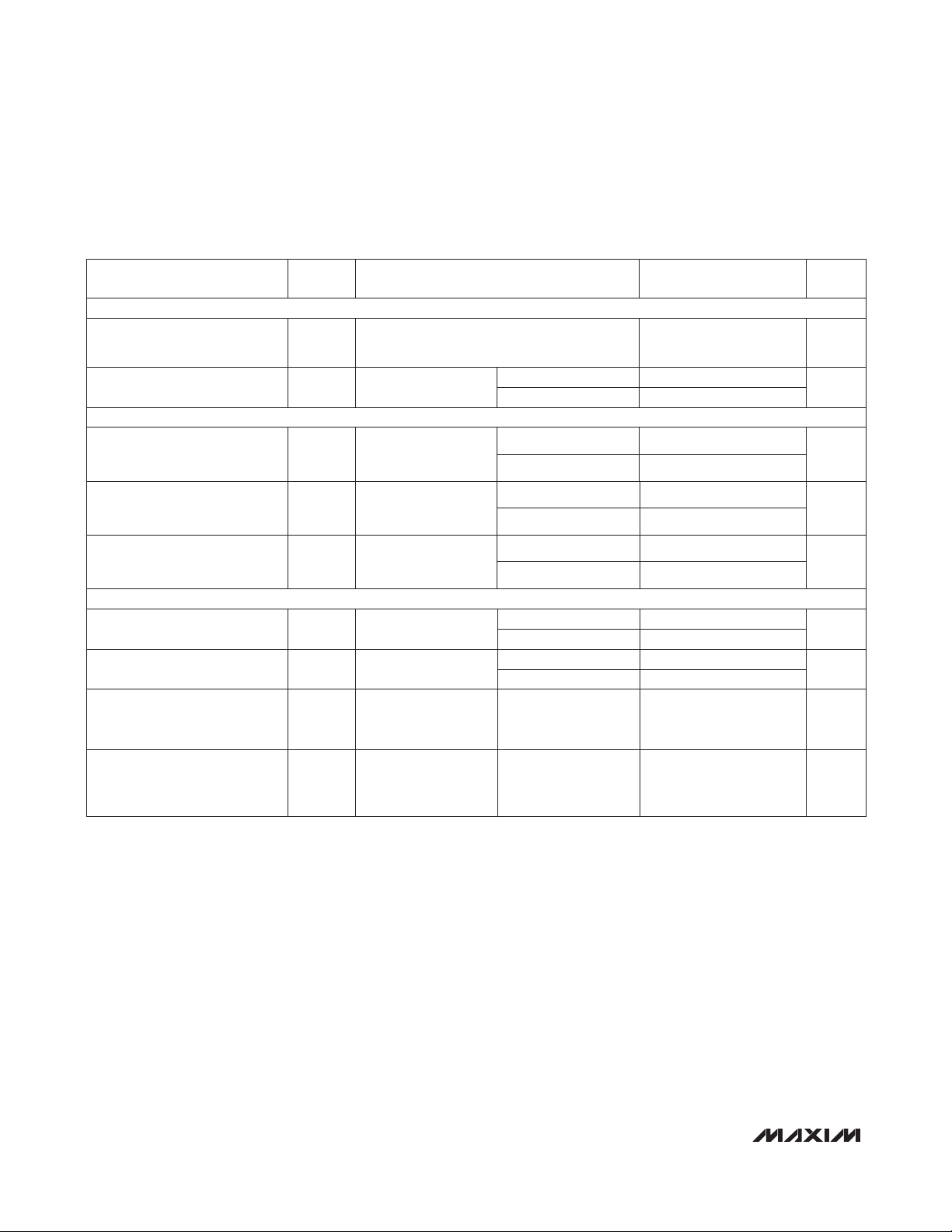
ELECTRICAL CHARACTERISTICS—Single Supply
(V+ = 12V, V- = 0V, VL = 5V, GND = 0V, V
INH
= 2.4V, V
INL
= 0.8V, TA= T
MIN
to T
MAX
, unless otherwise noted.)
Note 2: The algebraic convention, where the most negative value is a minimum and the most positive value a maximum, is used in
this data sheet.
Note 3: Guaranteed by design.
Note 4: ΔR
ON
= ΔRONmax - ΔRONmin.
Note 5: Flatness is defined as the difference between the maximum and minimum value of on-resistance as measured over the
specified analog signal range.
Note 6: Leakage parameters are 100% tested at maximum-rated hot temperature and guaranteed by correlation at +25°C.
Note 7: Off isolation = 20log
10[VCOM
/ (VNCor VNO)], V
COM
= output, VNCor VNO= input to off switch.
Note 8: Between any two switches.
Note 9: Leakage testing at single supply is guaranteed by testing with dual supplies.
(Note 3)
CONDITIONS
V0V+
V
COM
_,
VNO_,
VNC_
Analog Signal Range
UNITS
MIN TYP MAX
(Note 2)
SYMBOLPARAMETER
12.5 25
I
COM
= 10mA,
VNC_ or VNO_ +10V
R
ON
Channel On-Resistance
35
Ω
-1 0.0001 1
TA= +25°C
TA= T
MIN
to T
MAX
100 325
Figure 2,
V
NO
_ or VNC_ = 8V
ns
425
t
ON
Turn-On Time
(Note 3)
MAX314 only, Figure 3
RL= 300Ω,
CL= 35pF
t
D
Break-Before-Make Time Delay
(Note 3)
5 ns
I+Positive Supply Current
-5 5
µA
TA= +25°C
TA= T
MAX
V+ = 13.2V
all channels on or off,
VIN= 0V or 5V
-1 0.0001 1
VL= 5.5V
all channels on or off,
VIN= 0V or 5V
I
L
Logic Supply Current
-5 5
µA
TA= +25°C
TA= T
MAX
-1 -0.0001 1
VL= 5.5V
all channels on or off,
V
IN
= 0V or 5V
I
GND
Ground Current
-5 5
µA
TA= +25°C
TA= T
MAX
Figure 4,
C
L
= 1.0nF,
V
GEN
= 0V,
R
GEN
= 0V
V
CTE
Charge Injection
(Note 3)
-5 pC
TA= +25°C
TA= T
MIN
to T
MAX
TA= +25°C
TA= T
MIN
to T
MAX
95 175
Figure 2,
V
NO
_ or VNC_ = 8V
ns
225
t
OFF
Turn-Off Time
(Note 3)
TA= +25°C
TA= +25°C
ANALOG SWITCH
POWER SUPPLY
DYNAMIC
Page 5

MAX312/MAX313/MAX314
10ΩΩ, Quad, SPST, CMOS Analog Switches
_______________________________________________________________________________________
5
__________________________________________Typical Operating Characteristics
(TA = +25°C, unless otherwise noted.)
ON-RESISTANCE vs. V
(BIPOLAR SUPPLIES)
19
A: V+, V- = ±5V,
B: V+, V- = ±10V,
17
C: V+, V- = ±15V
15
13
(Ω)
ON
R
11
9
7
5
-15 -10 -5 105
ON-RESISTANCE vs. V
24
V+ = 12V,
22
V- = 0V
20
18
16
14
(Ω)
ON
12
R
10
8
6
4
2
024 108
015
V
(V)
COM
TEMPERATURE
A
B
C
D
E
61213 97511
V
(V)
COM
COM
A
B
AND
COM
A: TA = +125°C
= +85°C
B: T
A
= +70°C
C: T
A
= +25°C
D: T
A
= -55°C
E: T
A
ON-RESISTANCE vs. V
TEMPERATURE
16
14
V+ = 15V,
V+ = -15V
MAX312-01
12
10
(Ω)
ON
R
8
C
6
4
2
-15 -10 -5 105
015
V
(V)
COM
OFF LEAKAGE CURRENT
vs. TEMPERATURE
100
MAX312-04
OFF LEAKAGE (nA)
V+ = 15V,
V- = -15V,
10
OR VNO = ±10V
V
NC
= ±10V
V
COM
1
0.1
0.01
0.001
0.0001
-25 0 75
-50 125
25
TEMPERATURE (°C)
COM
A: TA = +125°C
B: T
A
C: T
A
D: T
A
E: T
A
A
B
C
D
E
50
AND
= +85°C
= +70°C
= +25°C
= -55°C
100
MAX312-02
MAX312 TOC05
ON-RESISTANCE vs. V
(SINGLE SUPPLY, V- = 0V)
(Ω)
R
1000
100
ON
10
A
B
C
D
1
24
01 3 5 15
79
6810
V
(V)
COM
ON LEAKAGE CURRENT
vs. TEMPERATURE
100
V+ = 15V,
V- = -15V,
10
0.1
ON LEAKAGE (nA)
0.01
0.001
0.0001
= ±10V
V
COM
1
-25 0 75
-50 125
50
25
TEMPERATURE (°C)
COM
A: V+ = 2.7V
B: V+ = 3.3V
C: V+ = 5V
D: V+ = 9V
E: V+ = 12V
F: V+ = 15V
E
12 14
11 13
100
F
MAX312-03
MAX312 TOC06
40
A: V+ = 15V, V- = -15V
B: V+ = 12V, V- = 0V
30
20
10
(pc)
0
CTE
V
-10
-20
-30
-40
CHARGE INJECTION
vs. V
-12 -8 40
-4 8 10 12 14-14 -10 2-2-6 6
V
COM
COM
(V)
100
MAX312-07
A
B
10
1
(μA)
L
0.1
I+, I-, I
0.01
0.001
0.0001
SUPPLY CURRENT
vs. TEMPERATURE
A: I+ = 16.5V
B: I- = -16.5V
= 5.5V
C: I
L
A
B
C
-25 0 75
-50-75 125
25
50
TEMPERATURE (°C)
100
MAX312 TOC08
Page 6

MAX312/MAX313/MAX314
10ΩΩ, Quad, SPST, CMOS Analog Switches
6 _______________________________________________________________________________________
______________________________________________________________Pin Description
Logic Supply Voltage1212
Analog Signal Normally Open Terminals——
Analog Signal Normally Closed Terminals——
Negative Analog Supply Input (connect to GND for single-supply operation)44
Logic Level Ground55
Analog Signal Normally Open Terminals
3, 6,
11, 14
—
Analog Signal Normally Closed Terminals—
3, 6,
11, 14
Analog Signal Common Terminals
2, 7,
10, 15
2, 7,
10, 15
Logic Level Inputs
1, 8,
9, 16
1, 8,
9, 16
FUNCTION
12
3, 6
11, 14
4
5
—
—
2, 7,
10, 15
1, 8,
9, 16
PIN
VL
NO1, NO4
NC3, NC2
V-
GND
NO1, NO4,
NO3, NO2
NC1, NC4,
NC3, NC2
COM1, COM4,
COM3, COM2
IN2, IN4,
IN3, IN2
NAME
Positive Analog Supply Input1313 13 V+
MAX312 MAX313 MAX314
____________________________Typical Operating Characteristics (continued)
(TA = +25°C, unless otherwise noted.)
0
-120
10 100 1000 10000 100000
TOTAL HARMONIC DISTORTION
vs. FREQUENCY
-80
-100
MAX312-09
FREQUENCY (Hz)
DISTORTION (dB)
-60
-40
-20
100
.0001
.01
.001
DISTORTION (%)
.1
1
10
SIGNAL DISTORTION
MEASUREMENT LIMITS
V+ = 15V
V- = -15V
5V
RMS
SIGNAL
600Ω SOURCE AND LOAD
0
-80
1 10 100 300
FREQUENCY RESPONSE
-60
-70
MAX312-10
FREQUENCY (MHz)
LOSS (dB)
-50
-20
-30
-40
-10
20
-60
-40
-50
PHASE (degrees)
-30
0
-10
-20
10
ON
PHASE
ON RESPONSE
OFF ISOLATION
2.5pF CAPACITOR
(FOR REFERENCE ONLY)
Page 7

__________Applications Information
Low-Distortion Audio
The MAX312/MAX313/MAX314, having very low R
ON
and very low RONvariation with signal amplitude, are
well suited for low-distortion audio applications. The
Typical Operating Characteristics
show Total Harmonic
Distortion (THD) vs. Frequency graphs for several signal amplitudes and impedances. Higher source and
load impedances improve THD, but reduce off isolation.
Off Isolation at High Frequencies
In 50Ω systems, the high-frequency on-response of
these parts extends from DC to above 100MHz with a
typical loss of -2dB. When the switch is turned off, however, it behaves like a capacitor, and off isolation
decreases with increasing frequency. (Above 300MHz,
the switch actually passes more signal turned off than
turned on.) This effect is more pronounced with higher
source and load impedances.
Above 5MHz, circuit board layout becomes critical, and
it becomes difficult to characterize the response of the
switch independent of the circuit. The graphs shown in
the
Typical Operating Characteristics
were taken using
a 50Ω source and load connected with BNC connec-
tors to a circuit board deemed “average”; that is,
designed with isolation in mind, but not using strip-line
or other special RF circuit techniques. For critical applications above 5MHz, use the MAX440, MAX441, and
MAX442, which are fully characterized up to 160MHz.
MAX312/MAX313/MAX314
10ΩΩ, Quad, SPST, CMOS Analog Switches
_______________________________________________________________________________________ 7
Figure 1. Overvoltage Protection Using External Blocking
Diodes
Figure 2. Switching-Time Test Circuit
V+
V+
NO_
V
g
V-
V-
COM_
+3V
LOGIC
INPUT
SWITCH
OUTPUT
0V
0V
50%
V
O
0.9V
0
t
ON
LOGIC INPUT WAVEFORMS INVERTED FOR SWITCHES
THAT HAVE THE OPPOSITE LOGIC SENSE.
MAX312
MAX313
tr < 20ns
tf < 20ns
SWITCH
V
COM1
INPUT
t
OFF
0.9V
0
LOGIC
INPUT
+5V
VL
COM1
IN1
GND
0V
REPEAT TEST FOR EACH SWITCH. FOR LOAD
CONDITIONS, SEE Electrical Characteristics.
CL INCLUDES FIXTURE AND STRAY CAPACITANCE.
V
= V
O
COM (
RL + RON
RL
+15V
V+
NO1
OR NC1
V-
-15V
)
MAX314
R
L
300Ω
SWITCH
OUTPUT
C
L
35pF
V
O
Page 8

MAX312/MAX313/MAX314
10ΩΩ, Quad, SPST, CMOS Analog Switches
8 _______________________________________________________________________________________
Figure 3. Break-Before-Make Test Circuit (MAX314 only)
Figure 4. Charge Injection Test Circuit
LOGIC
INPUT
SWITCH
OUTPUT 1
(VO1)
SWITCH
OUTPUT 2
(VO2)
+3V
50%
0V
0.9V
01
0V
0.9V
02
0V
t
D
t
D
V
V
COM1
COM2
LOGIC
INPUT
= +10V
= +10V
+5V
VL
COM_
COM_
IN_
GND
C
INCLUDES FIXTURE AND STRAY CAPACITANCE.
L
+15V
V+
V-
-15V
NO_
NC_
MAX314
V
O1
R
V
O2
R
C
L2
L2
RL = 300Ω
= 35pF
C
L
C
L1
L1
MAX312
MAX313
MAX314
V
GEN
R
GEN
COM
+5V
VL
GND
IN
VIN = +3V
+15V
V+
NC OR
NO
V-
-15V
V
O
V
O
C
L
V
IN
OFF
V
OFF
IN
V
DEPENDS ON SWITCH CONFIGURATION;
IN
INPUT POLARITY DETERMINED BY SENSE OF SWITCH.
ON
ON
Q = (ΔVO)(CL)
ΔV
O
OFF
OFF
Page 9

MAX312/MAX313/MAX314
10ΩΩ, Quad, SPST, CMOS Analog Switches
_______________________________________________________________________________________ 9
Figure 5. Off-Isolation Test Circuit
Figure 6. Crosstalk Test Circuit
Figure 7. Channel-Off Capacitance Test Circuit
Figure 8. Channel-On Capacitance Test Circuit
+15V
C
SIGNAL
GENERATOR 0dBm
COM
ANALYZER
COM
NC OR NO
R
L
V+
GND
+5V
-15V
MAX312
MAX313
C
+15V
+5V
MAX314
VL
0V,
IN
V-
2.4V
C
SIGNAL
GENERATOR 0dBm
0V, 2.4V
ANALYZER
R
L
COM1
IN1
N02
V+
GND
VL
-15V
N01
IN2
COM2
V-
MAX312
MAX313
MAX314
50Ω
0V, 2.4V
NC
C
CAPACITANCE
METER
f = 1MHz
+15V
C
V+
COM
NC OR NO
GND
+5V
VL
V-
-15V
MAX312
MAX313
MAX314
CAPACITANCE
METER
IN
0V or
2.4V
C
f = 1MHz
+15V
C
V+
COM
NC OR NO
GND
+5V
VL
V-
-15V
MAX312
MAX313
MAX314
IN
0V or
2.4V
C
Page 10

MAX31
MAX312/MAX313/MAX314
10ΩΩ, Quad, SPST, CMOS Analog Switches
10 ______________________________________________________________________________________
___________________Chip TopographyOrdering Information (continued)
PART
MAX313CPE
MAX313CSE
MAX313C/D 0°C to +70°C
0°C to +70°C
0°C to +70°C
TEMP. RANGE PIN-PACKAGE
16 Plastic DIP
16 Narrow SO
Dice*
MAX313EPE
MAX313ESE -40°C to +85°C
-40°C to +85°C 16 Plastic DIP
16 Narrow SO
MAX313MJE -55°C to +125°C 16 CERDIP**
MAX314CPE
MAX314CSE
MAX314C/D 0°C to +70°C
0°C to +70°C
0°C to +70°C 16 Plastic DIP
16 Narrow SO
Dice*
MAX314EPE
MAX314ESE -40°C to +85°C
-40°C to +85°C 16 Plastic DIP
16 Narrow SO
MAX314MJE -55°C to +125°C 16 CERDIP**
* Contact factory for dice specifications.
**Contact factory for availability.
TRANSISTOR COUNT: 100
SUBSTRATE CONNECTED TO V+
PIN NAME PIN
NC1A
NC4B
NC3C
NC2D
A
B
C
D
NAME PIN NAME
ANO1
BNO4
CNO3
DNO2
NO1
NO4
NC3
NC2
MAX312 MAX313 MAX314
MAX313CUE 0°C to +70°C 16 TSSOP
MAX313EUE -40°C to +85°C 16 TSSOP
MAX314CUE 0°C to +70°C 16 TSSOP
MAX314EUE -40°C to +85°C 16 TSSOP
GND
V-
COM1 IN1 IN2 COM2
A
B
D
V+
(3.56mm)
V
L
C
0.140"
COM4 IN4 IN3
0.085"
(2.16mm)
COM3
Page 11

MAX312/MAX313/MAX314
10ΩΩ, Quad, SPST, CMOS Analog Switches
______________________________________________________________________________________ 11
Package Information
(The package drawing(s) in this data sheet may not reflect the most current specifications. For the latest package outline information,
go to www.maxim-ic.com/packages
.)
TSSOP4.40mm.EPS
PDIPN.EPS
Page 12

MAX312/MAX313/MAX314
10ΩΩ, Quad, SPST, CMOS Analog Switches
Maxim cannot assume responsibility for use of any circuitry other than circuitry entirely embodied in a Maxim product. No circuit patent licenses are
implied. Maxim reserves the right to change the circuitry and specifications without notice at any time.
12
____________________Maxim Integrated Products, 120 San Gabriel Drive, Sunnyvale, CA 94086 408-737-7600
© 2002 Maxim Integrated Products Printed USA is a registered trademark of Maxim Integrated Products.
Package Information (continued)
(The package drawing(s) in this data sheet may not reflect the most current specifications. For the latest package outline information,
go to www.maxim-ic.com/packages
.)
CDIPS.EPS
N
HE
1
TOP VIEW
D
C
L
e
FRONT VIEW
A
B
A1
SIDE VIEW
INCHES
DIM
A1
B
C
e 0.050 BSC 1.27 BSC
E
H 0.2440.228 5.80 6.20
VARIATIONS:
D
D
0∞-8∞
MAX
MIN
0.069
0.053A
0.010
0.004
0.019
0.014
0.007
0.010
0.150
0.157
0.016L
0.050
INCHES
MAX
MINDIM
0.189 0.197 AA5.004.80 8
0.337 0.344 AB8.758.55 14
0.3940.386D
PROPRIETARY INFORMATION
TITLE:
PACKAGE OUTLINE, .150" SOIC
MILLIMETERS
MIN
1.35
1.75
0.10
0.25
0.35
0.49
0.19
0.25
3.80 4.00
0.40 1.27
MILLIMETERS
MAX
MIN
9.80 10.00
21-0041
MAX
N MS012
16
REV.DOCUMENT CONTROL NO.APPROVAL
SOICN .EPS
AC
1
B
1
 Loading...