

Page 1
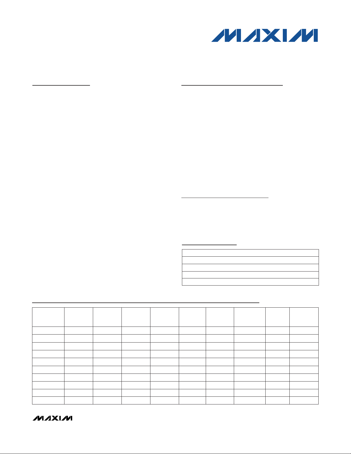
Selector Guide
*
Pin compatible with 75180, with additional features implemented using pins 1, 6, 8, and 13.
MAX3080E–MAX3089E
±15kV ESD-Protected, Fail-Safe, High-Speed (10Mbps),
Slew-Rate-Limited RS-485/RS-422 Transceivers
________________________________________________________________
Maxim Integrated Products
1
19-1800; Rev 1; 5/06
Ordering Information continued at end of data sheet.
Ordering Information
General Description
The MAX3080E–MAX3089E are ±15kV electrostatic discharge (ESD)-protected, high-speed transceivers for RS485/RS-422 communication that contain one driver and
one receiver. These devices feature fail-safe circuitry,
which guarantees a logic-high receiver output when the
receiver inputs are open or shorted. This means that the
receiver output will be a logic high if all transmitters on a
terminated bus are disabled (high impedance). The
MAX3080E/MAX3081E/MAX3082E feature reduced
slew-rate drivers that minimize EMI and reduce reflections caused by improperly terminated cables, allowing
error-free data transmission up to 115kbps. The
MAX3083E/MAX3084E/MAX3085E offer higher driver
output slew-rate limits, allowing transmit speeds up to
500kbps. The MAX3086E/MAX3087E/ MAX3088Es’ driver slew rates are not limited, making transmit speeds
up to 10Mbps possible. The MAX3089E’s slew rate is
selectable between 115kbps, 500kbps, and 10Mbps by
driving a selector pin with a single three-state driver. All
devices feature enhanced ESD protection. All transmitter
outputs and receiver inputs are protected to ±15kV
using the Human Body Model.
These transceivers typically draw 375µA of supply
current when unloaded, or when fully loaded with the drivers disabled.
All devices have a 1/8-unit-load receiver input impedance
that allows up to 256 transceivers on the bus. The
MAX3082E/MAX3085E/MAX3088E are intended for halfduplex communications, while the MAX3080E/MAX3081E/
MAX3083E/MAX3084E/MAX3086E/MAX3087E are
intended for full-duplex communications. The MAX3089E
is selectable between half-duplex and full-duplex operation. It also features independently programmable
receiver and transmitter output phase via separate pins.
Features
♦♦
ESD Protection for RS-485 I/O Pins
±15kV, Human Body Model
♦♦
True Fail-Safe Receiver While Maintaining
EIA/TIA-485 Compatibility
♦♦
Enhanced Slew-Rate Limiting Facilitates
Error- Free Data Transmission
(MAX3080E–MAX3085E/MAX3089E)
♦♦
1nA Low-Current Shutdown Mode (Except
MAX3081E/MAX3084E/MAX3087E)
♦♦
Pin-Selectable Full/Half-Duplex Operation
(MAX3089E)
♦♦
Phase Controls to Correct for Twisted-Pair
Reversal (MAX3089E)
♦♦
Allow Up to 256 Transceivers on the Bus
Applications
RS-422/RS-485 Communications
Level Translators
Transceivers for EMI-Sensitive Applications
Industrial-Control Local Area Networks
PART TEMP. RANGE PIN-PACKAGE
MAX3080ECSD
0°C to +70°C 14 SO
MAX3080ECPD 0°C to +70°C 14 Plastic DIP
MAX3080EESD -40°C to +85°C 14 SO
MAX3080EEPD -40°C to +85°C 14 Plastic DIP
Part
Half/Full
Duplex
Data
Rate
(Mbps)
Slew-
Rate
Limited
Low-
Power
Shutdown
Receiver/
Driver
Enable
Quiescent
Current
(µA)
Transceivers
On
Bus
Pin
Count
IndustryStandard
Pinout
7518014256375YesYesYes0.115
75179
75176
75180
75179
75176
75180
75179
75176
75180*14
8
8
14
8
8
14
8
8256
256
256
256
256
256
256
256
256375
375
375
375
375
375
375
375
375No
Yes
Yes
No
Yes
Yes
No
Yes
YesYes
Yes
No
Yes
Yes
No
Yes
Yes
NoYes
Yes
Yes
Yes
Yes
No
No
No
SelectableSelectable
10
10
10
0.5
0.5
0.5
0.115
0.115
Selectable
Half
Full
Full
Half
Full
Full
Half
Full
Full
MAX3080E
MAX3081E
MAX3082E
MAX3083E
MAX3084E
MAX3085E
MAX3086E
MAX3087E
MAX3088E
MAX3089E
For free samples and the latest literature, visit www.maxim-ic.com or phone 1-800-998-8800.
For small orders, phone 1-800-835-8769.
Page 2
MAX3080E–MAX3089E
±15kV ESD-Protected, Fail-Safe, High-Speed (10Mbps),
Slew-Rate-Limited RS-485/RS-422 Transceivers
2 _______________________________________________________________________________________
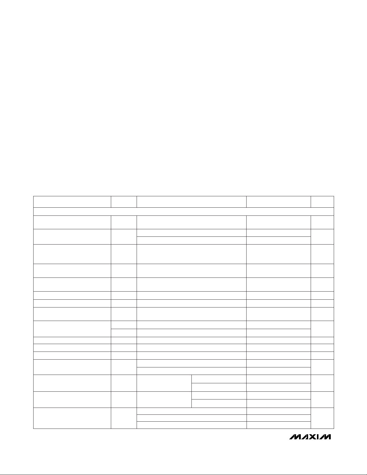
ABSOLUTE MAXIMUM RATINGS
DC ELECTRICAL CHARACTERISTICS
(VCC= +5V ±5%, TA= T
MIN
to T
MAX
, unless otherwise noted. Typical values are at VCC= +5V and TA= +25°C.) (Note 1)
Stresses beyond those listed under “Absolute Maximum Ratings” may cause permanent damage to the device. These are stress ratings only, and functional
operation of the device at these or any other conditions beyond those indicated in the operational sections of the specifications is not implied. Exposure to
absolute maximum rating conditions for extended periods may affect device reliability.
Supply Voltage (VCC) ............................................................+7V
Control Input Voltage (RE, DE)...................-0.3V to (V
CC
+ 0.3V)
Special Input Voltage
(H/F, SRL, TXP, RXP)..............................-0.3V to (V
CC
+ 0.3V)
Driver Input Voltage (DI).............................-0.3V to (V
CC
+ 0.3V)
Driver Output Voltage (A, B, Y, Z)........................................±13V
Receiver Input Voltage (A, B) ..............................................±13V
Receiver Input Voltage, Full Duplex (A, B) ..........................±25V
Receiver Output Voltage (RO)....................-0.3V to (V
CC
+ 0.3V)
Continuous Power Dissipation
8-Pin Plastic DIP (derate 9.09mW/°C above +70°C) ...727mW
8-Pin SO (derate 5.88mW/°C above +70°C)................471mW
14-Pin Plastic DIP (derate 10.0mW/°C above +70°C) ....800mW
14-Pin SO (derate 8.33mW/°C above +70°C)..............667mW
Operating Temperature Ranges
MAX308_EC_ _ ...................................................0°C to +70°C
MAX308_EE_ _ ................................................-40°C to +85°C
Storage Temperature Range .............................-65°C to +150°C
Lead Temperature (soldering, 10s) .................................+300°C
Figure 5, R = 50Ω (RS-422)
DE = GND,
V
CC
= GND or 5.25V
DE = GND,
VCC= GND or 5.25V
H/F, TXP, RXP, internal pulldown
DE, DI, RE
SRL = V
CC
SRL
MAX3080E–MAX3085E, and MAX3089E with
SRL = VCCor unconnected
DE, DI, RE, H/F, TXP, RXP
Figure 5, R = 50Ω or R = 27Ω
Figure 5, R = 50Ω or R = 27Ω
Figure 5, R = 50Ω or R = 27Ω
SRL (Note 3)
DE, DI, RE, H/F, TXP, RXP
SRL
CONDITIONS
µA
125
I
O
Output Leakage (Y and Z)
Full Duplex
µA
125
I
IN4
Input Current (A and B)
µA
75
I
IN3
SRL Input Current
V0.8V
IL2
Input Low Voltage
V0.4V
CC
0.6V
CC
V
IM2
Input Middle Voltage
VVCC- 0.8V
IH2
Input High Voltage
V
2.0
V
OD2
Differential Driver Output
10 40I
IN2
µA
±2I
IN1
SRL Input Current
mV100V
HYS
DI Input Hysteresis
V0.8V
IL1
Input Low Voltage
V0.2ΔV
OD
Change-in-Magnitude of
Differential Output Voltage
(Note 2)
V3V
OC
Driver Common-Mode Output
Voltage
V0.2ΔV
OC
Change-in-Magnitude of
Common-Mode Voltage (Note 2)
V2.0V
IH1
Input High Voltage
UNITSMIN TYP MAXSYMBOLPARAMETER
Figure 5, R = 27Ω (RS-485) 1.5
SRL = GND (Note 3) -75
VIN= 12V
VIN= 12V
VIN= -7V -100
-75VIN= -7V
Figure 5 V5V
OD1
Differential Driver Output
(No Load)
mAV
OD1
Driver Short-Circuit Output
Current (Note 4)
DRIVER
-7V ≤ V
OUT
≤ V
CC
-250
0V ≤ V
OUT
≤ 12V
0V ≤ V
OUT
≤ V
CC
±25
250
Page 3
MAX3080E–MAX3089E
±15kV ESD-Protected, Fail-Safe, High-Speed (10Mbps),
Slew-Rate-Limited RS-485/RS-422 Transceivers
_______________________________________________________________________________________ 3
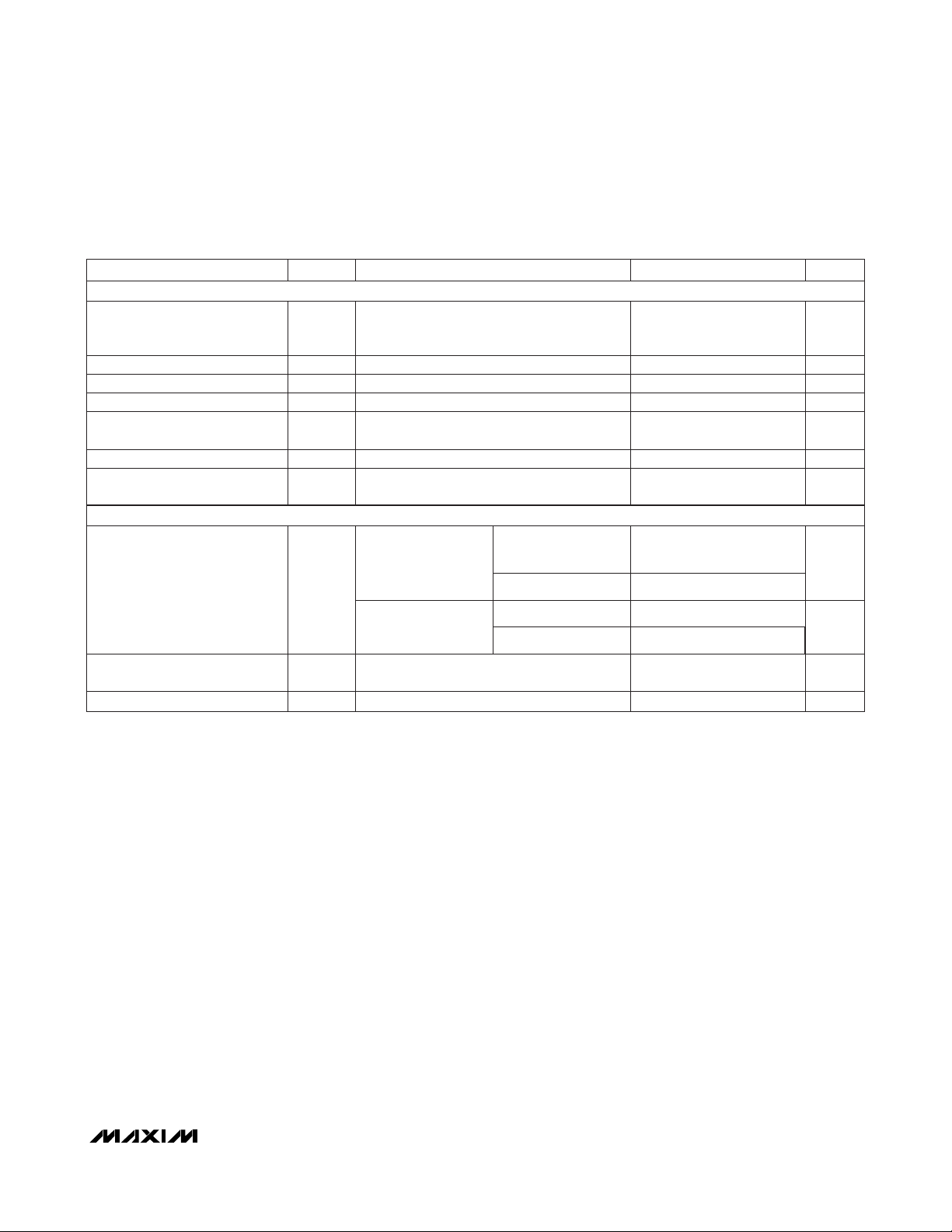
DC ELECTRICAL CHARACTERISTICS (continued)
(VCC= +5V ±5%, TA= T
MIN
to T
MAX
, unless otherwise noted. Typical values are at VCC= +5V and TA= +25°C.) (Note 1)
Note 1: All currents into the device are positive; all currents out of the device are negative. All voltages are referred to device
ground unless otherwise noted.
Note 2: ΔV
OD
and ΔVOCare the changes in VODand VOC, respectively, when the DI input changes state.
Note 3: The SRL pin is internally biased to V
CC
/ 2 by a 100kΩ/100kΩ resistor-divider. It is guaranteed to be V
CC
/ 2 if left
unconnected.
Note 4: Maximum current level applies to peak current just prior to foldback-current limiting; minimum current level applies during
current limiting.
375 600
430 900
DE = GND
DE = GND
475 1000
µA
420 800
DE = V
CC
DE = V
CC
No load,
RE = DI = GND
or V
CC
, SRL = GND
PARAMETER SYMBOL MIN TYP MAX UNITS
Receiver Output Low Voltage V
OL
0.4 V
Receiver Output High Voltage V
OH
VCC-1.5 V
Receiver Input Hysteresis ΔV
TH
25 mV
Receiver Differential Threshold
Voltage
V
TH
-200 -125 -50 mV
Three-State Output Current at
Receiver
I
OZR
±1 µA
Receiver Input Resistance R
IN
96 kΩ
Receiver Output Short-Circuit
Current
I
OSR
±7 ±95 mA
Supply Current I
CC
µA
Supply Current in Shutdown
Mode
I
SHDN
0.001 10 µA
CONDITIONS
No load,
RE = DI = GND
or V
CC
, SRL = V
CC
IO= 4mA, VID= -200mV
DE = GND, VRE= V
CC
IO= -4mA, VID= -50mV
-7V ≤ VCM≤ 12V
0.4V ≤ VO≤ 2.4V
-7V ≤ VCM≤ 12V
0V ≤ VRO≤ V
CC
ESD Protection for Y, Z, A, B ±15 kVHuman Body Model
RECEIVER
SUPPLY CURRENT
Page 4
MAX3080E–MAX3089E
±15kV ESD-Protected, Fail-Safe, High-Speed (10Mbps),
Slew-Rate-Limited RS-485/RS-422 Transceivers
4 _______________________________________________________________________________________
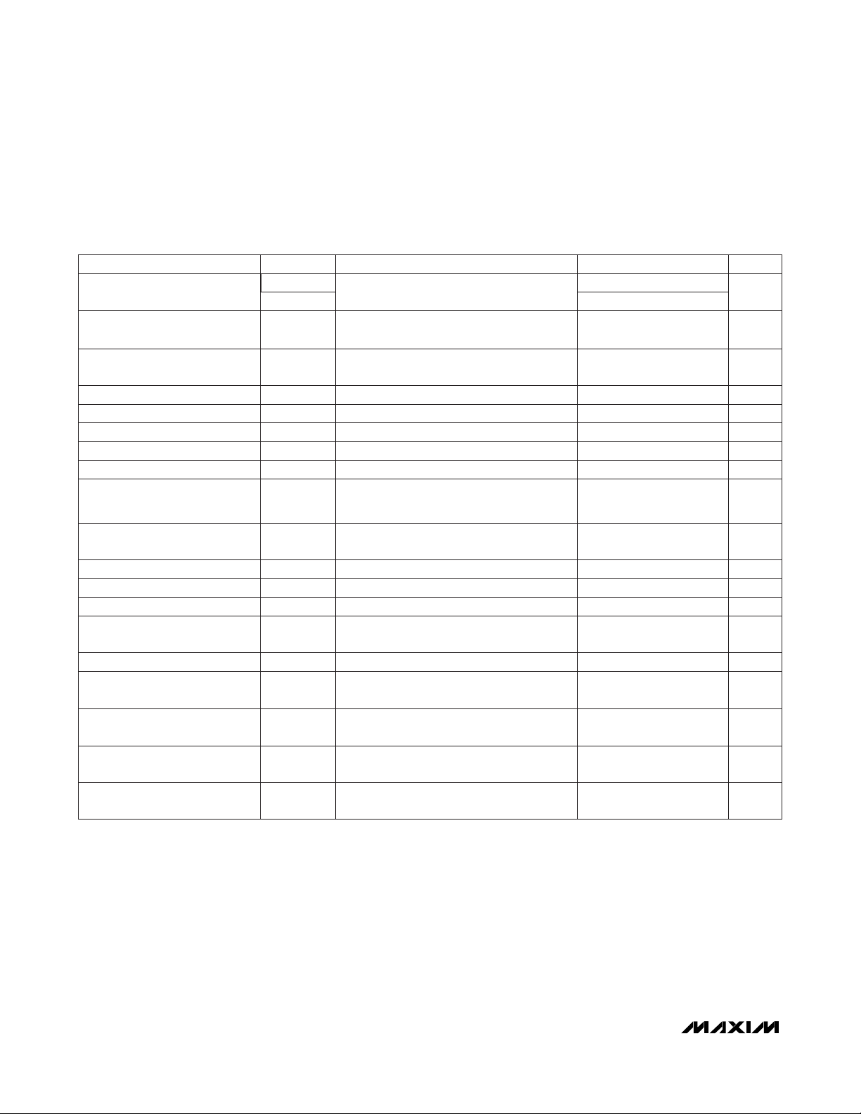
SWITCHING CHARACTERISTICS—MAX3080E/MAX3081E/MAX3082E, and MAX3089E
with SRL = Unconnected
(VCC= +5V ±5%, TA= T
MIN
to T
MAX
, unless otherwise noted. Typical values are at VCC= +5V and TA= +25°C.)
500 2030 2600
t
DPHL
PARAMETER SYMBOL MIN TYP MAX UNITS
Driver Disable Time from Low t
DLZ
100 ns
Driver Enable to Output Low t
DZL
3500 ns
Driver Enable to Output High t
DZH
3500 ns
Maximum Data Rate f
MAX
115 kbps
Driver Disable Time from High t
DHZ
100 ns
Receiver Input to Output
t
RPLH
,
t
RPHL
127 200 ns
|
t
RPLH
- t
RPHL
|
Differential
Receiver Skew
t
RSKD
3±30ns
Receiver Enable to Output Low t
RZL
20 50 ns
Driver Output Skew
|
t
DPLH
- t
DPHL |
Driver Input-to-Output
t
DPLH
500 2030 2600
ns
t
DSKEW
-3 ±200 ns
Driver Rise or Fall Time tDR, t
DF
667 1320 2500 ns
Receiver Enable to Output High t
RZH
20 50 ns
Receiver Disable Time from Low t
RLZ
20 50 ns
Receiver Disable Time from
High
t
RHZ
20 50 ns
Time to Shutdown t
SHDN
50 200 600 ns
Driver Enable from Shutdown to
Output High
t
DZH(SHDN)
6000 ns
Driver Enable from Shutdown to
Output Low
t
DZL(SHDN)
6000 ns
Receiver Enable from Shutdownto-Output High
t
RZH(SHDN)
3500 ns
Receiver Enable from Shutdownto-Output Low
t
RZL(SHDN)
3500 ns
CONDITIONS
Figures 6 and 12, CL= 100pF, S2 closed
Figures 8 and 10, CL= 15pF, S1 closed
Figures 6 and 12, CL= 100pF, S1 closed
Figures 8 and 10, CL= 100pF, S1 closed
Figures 8 and 10, CL= 100pF, S2 closed
Figures 8 and 10, CL= 15pF, S2 closed
Figures 11 and 13; |V
ID
|
≥ 2.0V;
rise and fall time of V
ID
≤ 15ns
Figures 6 and 12, CL= 100pF, S2 closed
(Note 5)
Figures 11 and 13; |V
ID
|
≥ 2.0V;
rise and fall time of V
ID
≤ 15ns
Figures 6 and 12, CL= 100pF, S1 closed
Figures 8 and 10, CL= 15pF, S2 closed
Figures 8 and 10, CL= 15pF, S1 closed
Figures 6 and 12, CL= 100pF, S2 closed
Figures 7 and 9, R
DIFF
= 54Ω,
CL1= CL2= 100pF
Figures 6 and 12, CL= 100pF, S1 closed
Figures 7 and 9, R
DIFF
= 54Ω,
C
L1
= CL2= 100pF
Figures 7 and 9, R
DIFF
= 54Ω,
C
L1
= CL2= 100pF
Page 5
MAX3080E–MAX3089E
±15kV ESD-Protected, Fail-Safe, High-Speed (10Mbps),
Slew-Rate-Limited RS-485/RS-422 Transceivers
_______________________________________________________________________________________ 5
SWITCHING CHARACTERISTICS—MAX3083E/MAX3084E/MAX3085E, and MAX3089E with
SRL = V
CC
(VCC= +5V ±5%, TA= T
MIN
to T
MAX
, unless otherwise noted. Typical values are at VCC= +5V and TA= +25°C.)
Receiver Enable from
Shutdown-to-Output Low
t
RZL(SHDN)
Figures 6 and 12, CL= 100pF, S1 closed 3500 ns
ns3500Figures 6 and 12, CL= 100pF, S2 closedt
RZH(SHDN)
Receiver Enable from
Shutdown-to-Output High
Driver Enable from
Shutdown-to-Output Low
t
DZL(SHDN)
Figures 8 and 10, CL= 15pF, S1 closed 4500 ns
ns4500Figures 8 and 10, CL= 15pF, S2 closedt
DZH(SHDN)
Driver Enable from
Shutdown-to-Output High
Time to Shutdown t
SHDN
(Note 5) 50 200 600 ns
ns20 50Figures 6 and 12, CL= 100pF, S2 closedt
RHZ
Receiver Disable Time from
High
Receiver Disable Time from Low t
RLZ
Figures 6 and 12, CL= 100pF, S1 closed 20 50 ns
ns20 50Figures 6 and 12, CL= 100pF, S2 closedt
RZH
Receiver Enable to Output High
Receiver Enable to Output Low t
RZL
Figures 6 and 12, CL= 100pF, S1 closed 20 50 ns
ns3±30
Figures 11 and 13; |V
ID
|
≥ 2.0V;
rise and fall time of V
ID
≤ 15ns
t
RSKD
|
t
RPLH
- t
RPHL
|
Differential
Receiver Skew
Receiver Input to Output
t
RPLH
,
t
RPHL
Figures 11 and 13; |V
ID
|
≥ 2.0V;
rise and fall time of V
ID
≤ 15ns
127 200 ns
ns100Figures 8 and 10, CL= 15pF, S2 closedt
DHZ
Driver Disable Time from High
Driver Disable Time from Low t
DLZ
Figures 8 and 10, CL= 15pF, S1 closed 100 ns
ns2500Figures 8 and 10, CL= 100pF, S1 closedt
DZL
Driver Enable to Output Low
Driver Enable to Output High t
DZH
Figures 8 and 10, CL= 100pF, S2 closed 2500 ns
kbps500f
MAX
Maximum Data Rate
Driver Rise or Fall Time t
DR, tDF
Figures 7 and 9, R
DIFF
= 54Ω,
C
L1
= CL2= 100pF
200 530 750 ns
ns-3 ±100
Figures 7 and 9, R
DIFF
= 54Ω,
CL1= CL2= 100pF
t
DSKEW
Driver Output Skew
|
t
DPLH
- t
DPHL |
Driver Input-to-Output
t
DPHL
t
DPLH
Figures 7 and 9, R
DIFF
= 54Ω,
CL1= CL2= 100pF
250 720 1000
250 720 1000
ns
UNITSMIN TYP MAXCONDITIONSSYMBOLPARAMETER
Page 6
MAX3080E–MAX3089E
±15kV ESD-Protected, Fail-Safe, High-Speed (10Mbps),
Slew-Rate-Limited RS-485/RS-422 Transceivers
6 _______________________________________________________________________________________
SWITCHING CHARACTERISTICS—MAX3086E/MAX3087E/MAX3088E, and MAX3089E with
SRL = GND
(VCC= +5V ±5%, TA= T
MIN
to T
MAX
, unless otherwise noted. Typical values are at VCC= +5V and TA= +25°C.)
Note 5: The device is put into shutdown by bringing RE high and DE low. If the enable inputs are in this state for less than 50ns, the
device is guaranteed not to enter shutdown. If the enable inputs are in this state for at least 600ns, the device is guaranteed
to have entered shutdown.
UNITSMIN TYP MAXCONDITIONSSYMBOLPARAMETER
Driver Input-to-Output
t
DPLH
t
DPHL
Figures 7 and 9, R
DIFF
= 54Ω,
CL1= CL2= 100pF
34 60
34 60
ns
ns-2.5 ±10
Figures 7 and 9, R
DIFF
= 54Ω,
CL1= CL2= 100pF
t
DSKEW
Driver Output Skew
|
t
DPLH
- t
DPHL |
Driver Rise or Fall Time t
DR, tDF
Figures 7 and 9, R
DIFF
= 54Ω,
C
L1
= CL2= 100pF
14 25 ns
Maximum Data Rate f
MAX
10 Mbps
Driver Enable to Output High t
DZH
Figures 8 and 10, CL= 100pF, S2 closed 150 ns
ns150Figures 8 and 10, CL= 100pF, S1 closedt
DZL
Driver Enable to Output Low
Driver Disable Time from Low t
DLZ
Figures 8 and 10, CL= 15pF, S1 closed 100 ns
ns100Figures 8 and 10, CL= 15pF, S2 closedt
DHZ
Driver Disable Time from High
Receiver Input-to-Output
t
RPLH
,
t
RPHL
Figures 11 and 13; |V
ID
|
≥ 2.0V;
rise and fall time of V
ID
≤ 15ns
106 150 ns
ns0±10
Figures 11 and 13; |V
ID |
≥ 2.0V;
rise and fall time of V
ID
≤ 15ns
t
RSKD
|
t
RPLH
- t
RPHL |
Differential
Receiver Skew
t
RZL
Figures 6 and 12, CL= 100pF, S1 closed 20 50 ns
ns
ns
ns
ns
ns
ns
ns
ns3500
3500
250
250
50 200 600
20 50
20 50
20 50Figures 6 and 12, CL= 100pF, S2 closed
Figures 6 and 12, CL= 100pF, S1 closed
Figures 6 and 12, CL= 100pF, S2 closed
(Note 5)
Figures 8 and 10, CL= 15pF, S2 closed
Figures 8 and 10, CL= 15pF, S1 closed
Figures 6 and 12, CL= 100pF, S2 closed
Figures 6 and 12, CL= 100pF, S1 closedt
RZL(SHDN)
t
RZH(SHDN)
t
DZL(SHDN)
t
DZH(SHDN)
t
SHDN
t
RHZ
t
RLZ
t
RZH
Receiver Enable to Output Low
Receiver Enable to Output High
Receiver Disable Time from Low
Receiver Disable Time from
High
Time to Shutdown
Driver Enable from
Shutdown-to-Output High
Driver Enable from
Shutdown-to-Output Low
Receiver Enable from
Shutdown-to-Output High
Receiver Enable from
Shutdown-to-Output Low
Page 7
MAX3080E–MAX3089E
±15kV ESD-Protected, Fail-Safe, High-Speed (10Mbps),
Slew-Rate-Limited RS-485/RS-422 Transceivers
_______________________________________________________________________________________
7
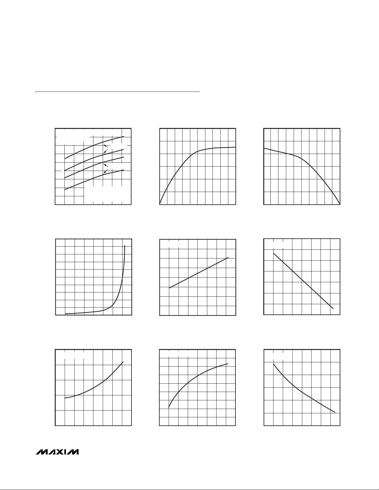
Typical Operating Characteristics
(VCC= +5V, TA = +25°C, unless otherwise noted.)
NO-LOAD SUPPLY CURRENT
vs. TEMPERATURE
525
A: MAX3086E/MAX3087E/MAX3088E,
MAX3089E WITH
500
SRL = GND
475
450
A
425
B
400
A
375
350
NO-LOAD SUPPLY CURRENT (μA)
B
325
300
-60 100
-40 -20 20 80
B: MAX3080E–MAX3085E,
MAX3089E WITH
SRL = OPEN OR V
40
060
TEMPERATURE (°C)
DE = V
DE = GND
CC
CC
MAX3080/3089 TOC-16
OUTPUT CURRENT (mA)
SHUTDOWN CURRENT
vs. TEMPERATURE
20
18
16
14
12
10
8
6
SHUTDOWN CURRENT (nA)
4
2
0
-60 100
-40 -20 20 80
TEMPERATURE (°C)
40
060
MAX3080/3089 TOC-1
OUTPUT LOW VOLTAGE (V)
vs. RECEIVER OUTPUT LOW VOLTAGE
OUTPUT CURRENT
60
50
40
30
20
10
0
05
14
OUTPUT LOW VOLTAGE (V)
3
2
30
25
MAX3080/3089 TOC-2
20
15
10
OUTPUT CURRENT (mA)
5
0
05
RECEIVER OUTPUT LOW VOLTAGE
vs. TEMPERATURE
0.50
IRO = 8mA
0.45
0.40
0.35
0.30
0.25
0.20
0.15
0.10
-60 80 100
-40 -20 60
20
040
TEMPERATURE (°C)
4.5
4.4
MAX3080/3089 TOC-5
4.3
4.2
4.1
OUTPUT VOLTAGE (V)
4.0
3.9
3.8
-60 80 100
OUTPUT CURRENT
vs. RECEIVER OUTPUT HIGH VOLTAGE
14
OUTPUT HIGH VOLTAGE (V)
RECEIVER OUTPUT HIGH VOLTAGE
vs. TEMPERATURE
IRO = 8mA
-40 -20 60
3
2
20
040
TEMPERATURE (°C)
MAX3080/3089 TOC-3
MAX3080/3089 TOC-4
RECEIVER PROPAGATION DELAY
(500kbps MODE) vs. TEMPERATURE
140
C
= 100pF
LOAD
135
130
125
PROPAGATION DELAY (ns)
120
115
-60 100
-40 -20 20 80
TEMPERATURE (°C)
40
060
112
110
MAX3080/3089 TOC-7
108
106
104
102
100
PROPAGATION DELAY (ns)
98
96
94
-60 100
RECEIVER PROPAGATION DELAY
(10Mbps MODE) vs. TEMPERATURE
C
= 100pF
LOAD
40
-40 -20 20 80
060
TEMPERATURE (°C)
MAX3080/3089 TOC-8
PROPAGATION DELAY (μs)
DRIVER PROPAGATION DELAY
(115kbps MODE) vs. TEMPERATURE
2.20
Rt = 54Ω
2.15
2.10
2.05
2.00
1.95
1.90
-60 100
-40 -20 20 80
TEMPERATURE (°C)
40
060
MAX3080/3089 TOC-9
Page 8
MAX3080E–MAX3089E
±15kV ESD-Protected, Fail-Safe, High-Speed (10Mbps),
Slew-Rate-Limited RS-485/RS-422 Transceivers
8 _______________________________________________________________________________________
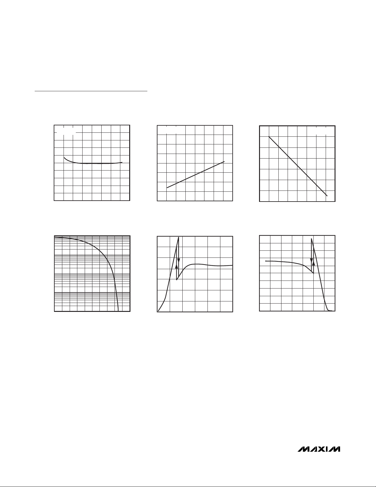
Typical Operating Characteristics (continued)
(VCC= +5V, TA = +25°C, unless otherwise noted.)
520
560
-60 100
DRIVER PROPAGATION DELAY
(500kbps MODE) vs. TEMPERATURE
600
640
920
MAX3080/3089 TOC-10
TEMPERATURE (°C)
PROPAGATION DELAY (ns)
40
760
800
720
680
060
840
880
-40 -20 20 80
Rt = 54Ω
20
25
-60 100
DRIVER PROPAGATION DELAY
(10Mbps MODE) vs. TEMPERATURE
30
60
MAX3080/3089 TOC-11
TEMPERATURE (°C)
PROPAGATION DELAY (ns)
40
45
50
40
35
060
55
-40 -20 20 80
Rt = 54Ω
DRIVER OUTPUT CURRENT
vs. DIFFERENTIAL OUTPUT VOLTAGE
100
10
1
OUTPUT CURRENT (mA)
0.1
0.01
01
DIFFERENTIAL OUTPUT VOLTAGE (V)
234 5
MAX3080 TOC-12
OUTPUT CURRENT (mA)
DRIVER OUTPUT LOW VOLTAGE
140
120
100
80
60
40
20
0
024681012
OUTPUT CURRENT vs.
OUTPUT LOW VOLTAGE (V)
DRIVER DIFFERENTIAL OUTPUT VOLTAGE
1.90
1.89
1.88
1.87
1.86
OUTPUT VOLTAGE (V)
1.85
1.84
1.83
-60 100
-100
-90
MAX3080-25
-80
-70
-60
-50
-40
-30
OUTPUT CURRENT (mA)
-20
-10
0
-8 -2
vs. TEMPERATURE
Rt = 54Ω
40
-40 -20 20 80
060
TEMPERATURE (°C)
OUTPUT CURRENT vs.
DRIVER OUTPUT HIGH VOLTAGE
OUTPUT HIGH VOLTAGE (V)
MAX3080/3089 TOC-13
MAX3080/3089 TOC-27
642-6 -4 0
Page 9
MAX3080E–MAX3089E
±15kV ESD-Protected, Fail-Safe, High-Speed (10Mbps),
Slew-Rate-Limited RS-485/RS-422 Transceivers
_______________________________________________________________________________________
9
Typical Operating Characteristics (continued)
(VCC= +5V, TA = +25°C, unless otherwise noted.)
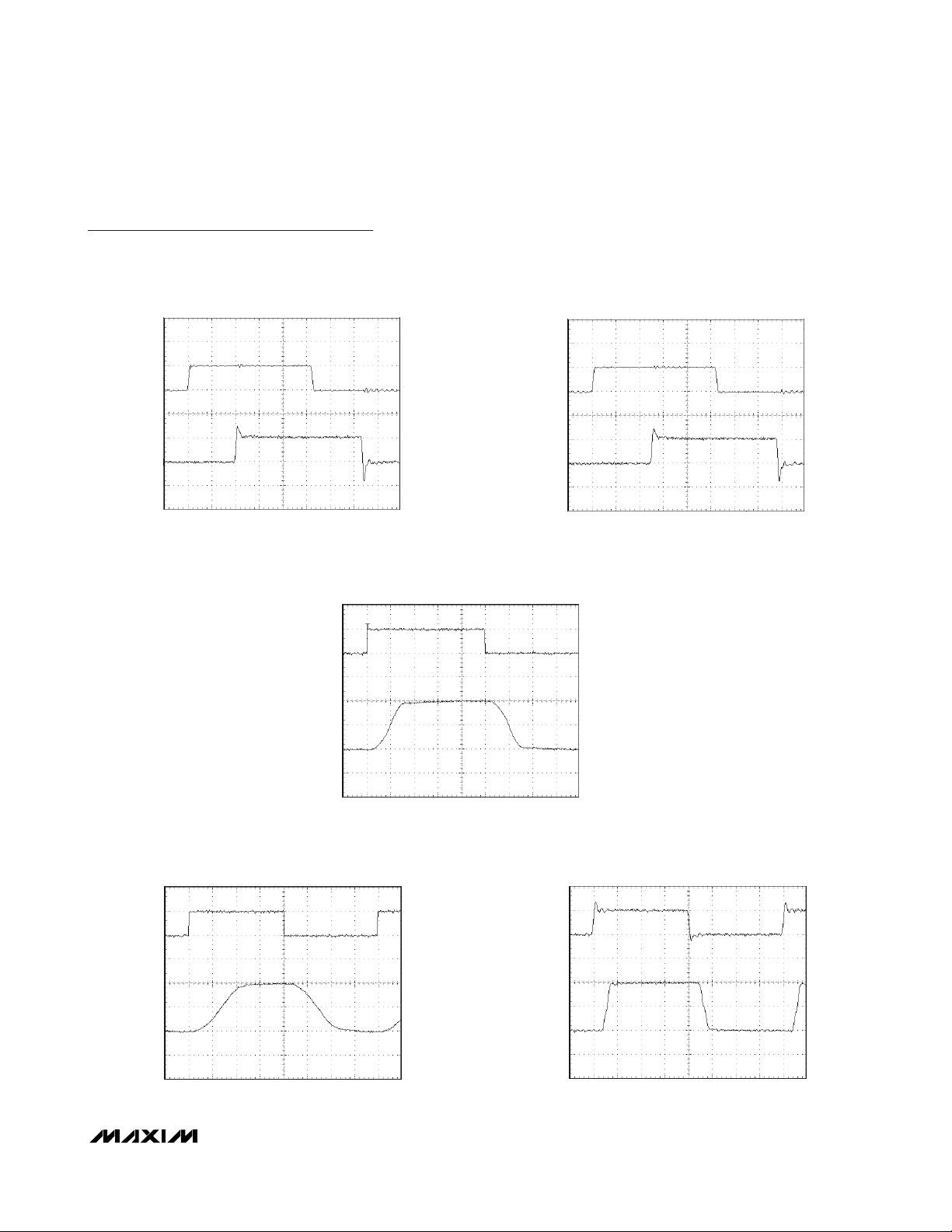
RECEIVER PROPAGATION DELAY
MAX3086E/MAX3087E/MAX3088E AND MAX3089E
VA - V
WITH SRL = GND
B
RO
50ns/div
MAX3080/3089 TYP-18
MAX3080E/MAX3081E/MAX3082E AND MAX3089E
DI
RECEIVER PROPAGATION DELAY
MAX3080E–MAX3085E AND MAX3089E
2V/div
5V/div
DRIVER PROPAGATION DELAY
WITH SRL = OPEN
VA - V
B
RO
MAX3080/3089 TYP-20
WITH SRL = OPEN OR V
50ns/div
5V/div
CC
MAX3080/3089 TYP-17
2V/div
5V/div
V
- V
Y
Z
DRIVER PROPAGATION DELAY
MAX3083E/MAX3084E/MAX3085E AND MAX3089E
WITH SRL = V
DI
- V
V
Y
Z
CC
500ns/div
MAX3080/3089 TYP-21
5V/div
2.5V/div
2μs/div
2.5V/div
DRIVER PROPAGATION DELAY
MAX3086E/MAX3087E/MAX3088E AND MAX3089E
WITH SRL = GND
DI
- V
V
Y
Z
50ns/div
MAX3080/3089 TYP-22
5V/div
2.5V/div
Page 10
MAX3080E–MAX3089E
±15kV ESD-Protected, Fail-Safe, High-Speed (10Mbps),
Slew-Rate-Limited RS-485/RS-422 Transceivers
10 ______________________________________________________________________________________
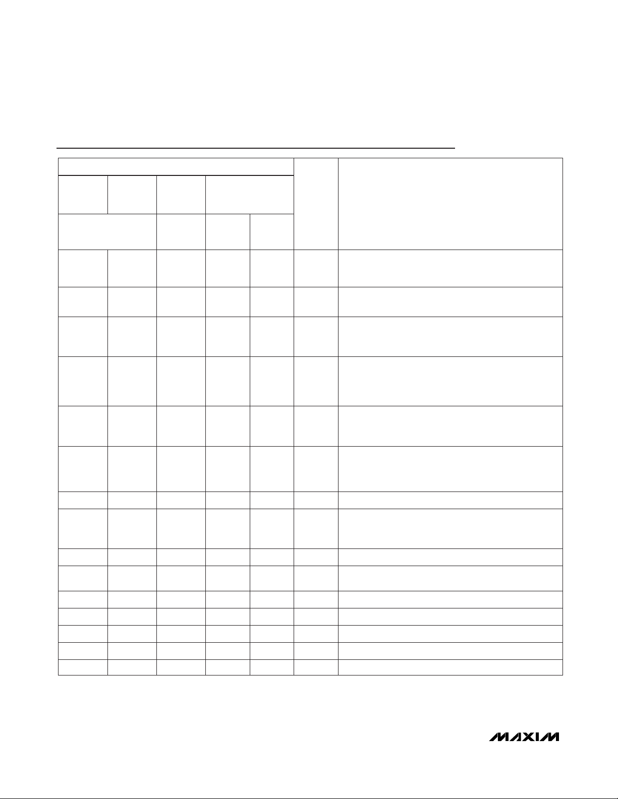
Pin Description
MAX3081E
MAX3084E
MAX3087E
MAX3080E
MAX3083E
MAX3086E
MAX3082E
MAX3085E
MAX3088E
FULL-DUPLEX
DEVICES
HALF-
DUPLEX
MODE
FULL-
DUPLEX
MODE
HALF-
DUPLEX
DEVICES
—95 — Noninverting Driver OutputY9
5
6
7
5
6
7
3
—
4
4
—
5
Driver Input. With DE high, a low on DI forces noninverting
output low and inverting output high. Similarly, a high on DI
forces non-inverting output high and inverting output low.
DI5
Slew-Rate-Limit Selector Pin. Connect SRL to GND for
10Mbps communication rate; connect to VCCfor
500kbps communication rate. Leave unconnected for
115kbps communication rate.
SRL—
GroundGND6, 7
88— — TXP—
44— 3
Driver Output Enable. Drive DE high to enable driver outputs. These outputs are high impedance when DE is low.
Drive RE high and DE low to enter low-power shutdown
mode.
DE4
2
3
1
2
3
1
2
—
—
1
2
—
Receiver Output. When RE is low and if A - B ≥ -50mV,
RO will be high; if A - B ≤ -200mV, RO will be low.
RO2
Receiver Output Enable. Drive RE low to enable RO; RO
is high impedance when RE is high. Drive RE high and
DE low to enter low-power shutdown mode.
RE
3
FUNCTIONNAME
Half/Full-Duplex Selector Pin. Connect H/F to VCCfor halfduplex mode; connect to GND or leave unconnected for
full-duplex mode.
H/F
—
Transmitter Phase. Connect TXP to GND, or leave floating
for normal transmitter phase/polarity. Connect to V
CC
to
invert the transmitter phase/polarity.
— — — — 9 Y
Noninverting Receiver Input and Noninverting Driver
Output*
10 6 — 10 — Z Inverting Driver Output
— — — — 10 Z Inverting Receiver Input and Inverting Driver Output*
11 7 — 11 — B Inverting Receiver Input
—
—
— — — 11 B Receiver Input Resistors*
— 7 — — B Inverting Receiver Input and Inverting Driver Output
MAX3089E
PIN
Page 11
MAX3080E–MAX3089E
±15kV ESD-Protected, Fail-Safe, High-Speed (10Mbps),
Slew-Rate-Limited RS-485/RS-422 Transceivers
______________________________________________________________________________________ 11
Pin Description (continued)
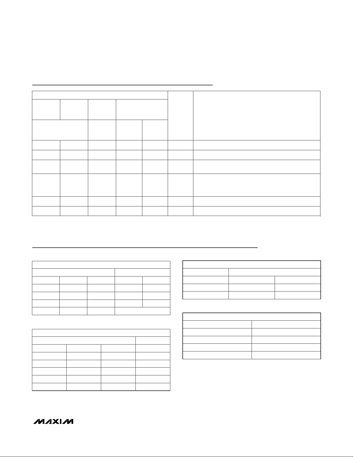
Function Tables
TRANSMITTING
INPUTS OUTPUTS
RE
DE DI Z Y
X 1 1 0 1
X 1 0 1 0
0 0 X High- Z High-Z
1 0 X Shutdown
RECEIVING
INPUTS OUTPUT
RE
DE A - B RO
0 X ≥ -0.05V 1
0 X ≤ -0.2V 0
0 X Open/shorted 1
1 1 X High- Z
1 0 X Shutdown
TRANSMITTING
INPUT OUTPUTS
DI Z Y
1 0 1
0 1 0
RECEIVING
INPUTS OUTPUT
A - B RO
≥ -0.05V 1
≤ -0.2V 0
Open/shorted 1
X = Don’t care
Shutdown mode, driver and receiver outputs high impedance
*
(MAX3089E only). In half-duplex mode, the driver outputs serve as receiver inputs. The full-duplex receiver inputs (A and B) will still
have a 1/8-unit load, but are not connected to the receiver.
MAX3081E/MAX3084E/MAX3087EMAX3080E/MAX3083E/MAX3086E
FUNCTIONNAME
Not Connected. Not internally connected.N.C.————1, 8, 13
Positive Supply 4.75V ≤ VCC≤ 5.25VV
CC
14148114
Receiver Phase. Connect RXP to GND, or leave unconnected for normal receiver phase/polarity. Connect to
V
CC
to invert the receiver phase/polarity.
RXP1313———
Noninverting Receiver Input and Noninverting Driver
Output
A——6——
Receiver Input Resistors*
HALF-
DUPLEX
DEVICES
FULL-
DUPLEX
MODE
HALF-
DUPLEX
MODE
A12————
Noninverting Receiver InputA—12—812
MAX3081E
MAX3084E
MAX3087E
MAX3080E
MAX3083E
MAX3086E
MAX3082E
MAX3085E
MAX3088E
MAX3089E
FULL-DUPLEX
DEVICES
PIN
Page 12
MAX3080E–MAX3089E
±15kV ESD-Protected, Fail-Safe, High-Speed (10Mbps),
Slew-Rate-Limited RS-485/RS-422 Transceivers
12 ______________________________________________________________________________________
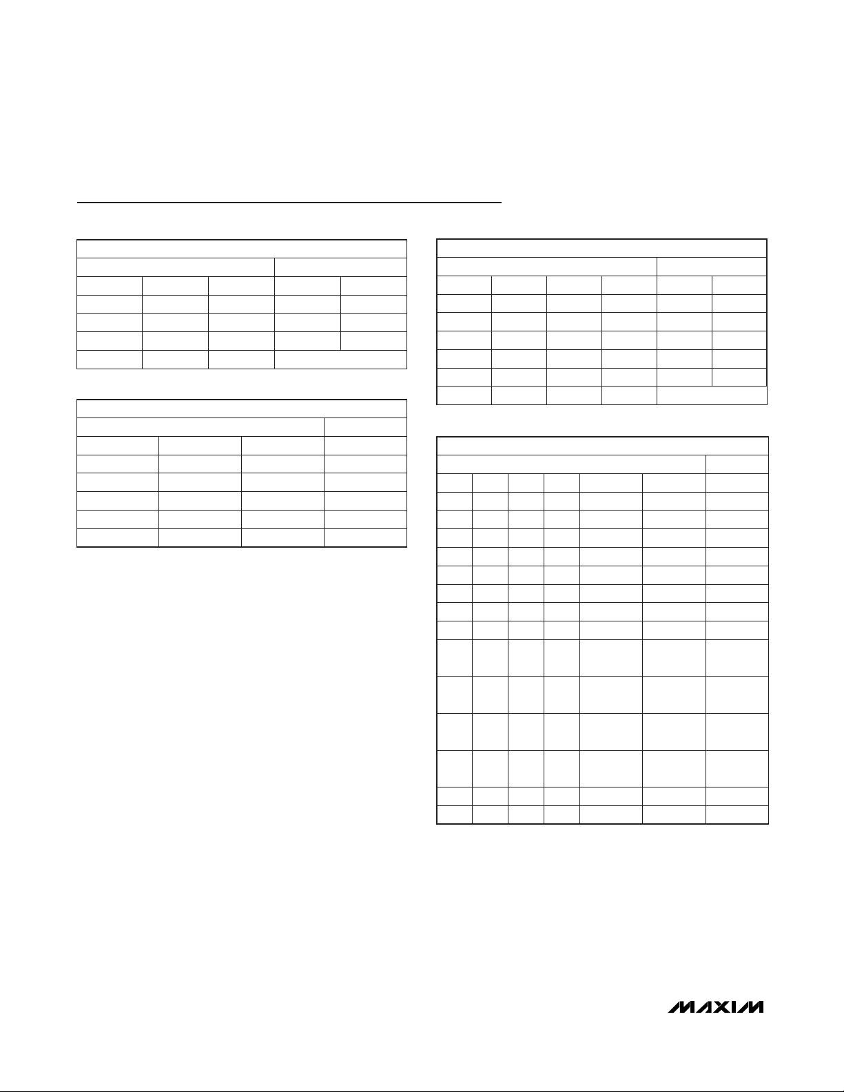
Function Tables (continued)
TRANSMITTING
INPUTS OUTPUTS
RE
DE DI B/Z A/Y
X 1 1 0 1
X 1 0 1 0
0 0 X High- Z High-Z
1 0 X Shutdown
RECEIVING
INPUTS OUTPUT
RE
DE A - B RO
0 X ≥ -0.05V 1
0 X ≤ -0.2V 0
0 X Open/shorted 1
1 1 X High- Z
1 0 X Shutdown
MAX3089E
TRANSMITTING
INPUTS OUTPUTS
TXP
RE
DE DI Z Y
0 X 1 1 0 1
0 X 1 0 1 0
1 X 1 1 1 0
1 X 1 0 0 1
X 0 0 X High- Z High-Z
X 1 0 X Shutdown
INPUTS OUTPUT
H/F
RXP
RE
DE A - B Y - Z RO
0 0 0 X ≥ -0.05V X 1
0 0 0 X ≤ -0.2V X 0
0 1 0 X ≥ -0.05V X 0
0 1 0 X ≤ -0.2V X 1
1 0 0 0 X ≥ -0.05V 1
1 0 0 0 X ≤ -0.2V 0
1 1 0 0 X ≥ -0.05V 0
1 1 0 0 X ≤ -0.2V 1
0 0 0 X
Open/
shorted
X 1
1 0 0 0 X
Open/
shorted
1
0 1 0 X
Open/
shorted
X 0
1 1 0 0 X
Open/
shorted
0
X X 1 1 X X High-Z
X X 1 0 X X Shutdown
RECEIVING
X = Don’t care
Shutdown mode, driver and receiver outputs high impedance
MAX3082E/MAX3085E/MAX3088E
Page 13
MAX3080E–MAX3089E
±15kV ESD-Protected, Fail-Safe, High-Speed (10Mbps),
Slew-Rate-Limited RS-485/RS-422 Transceivers
______________________________________________________________________________________ 13
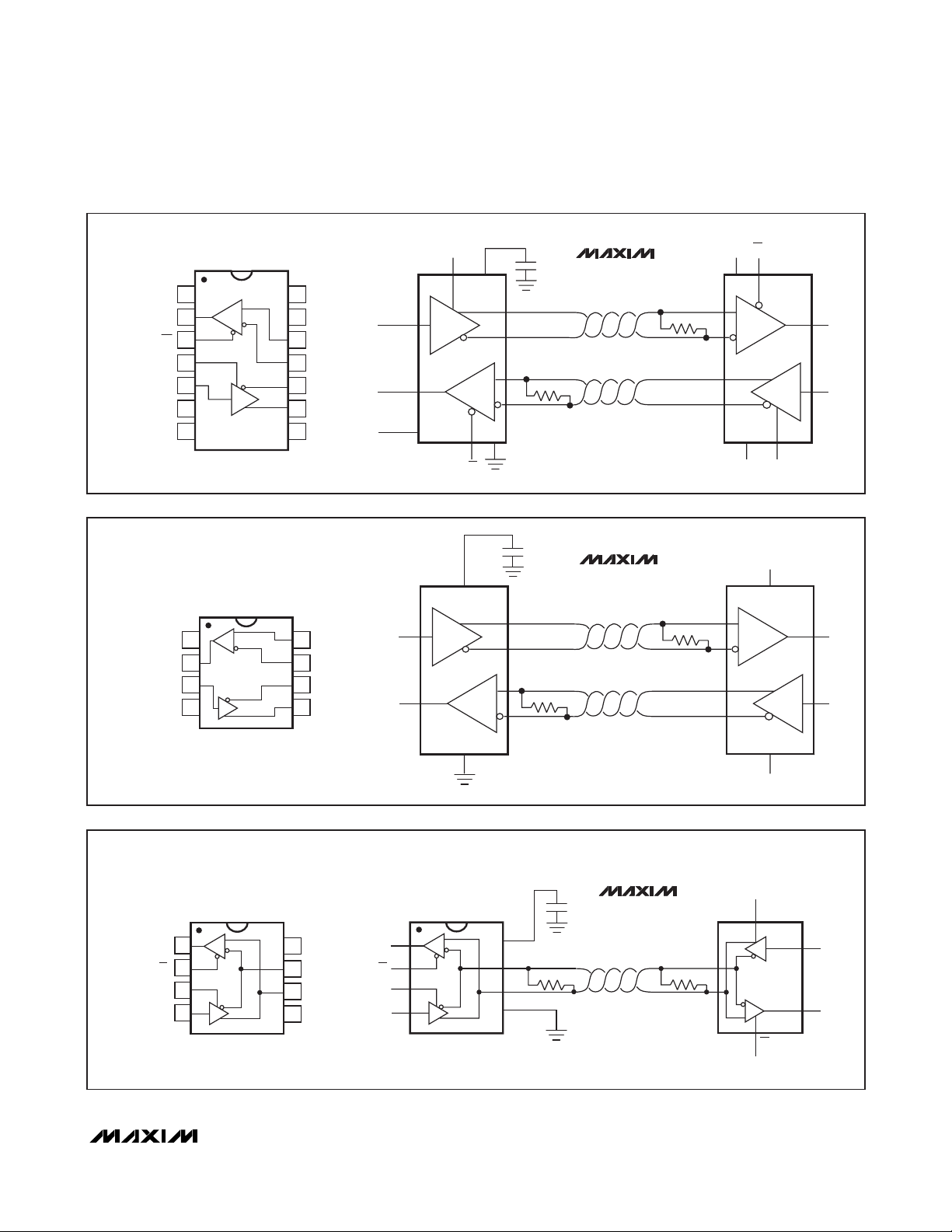
Figure 2. MAX3081E/MAX3084E/MAX3087E Pin Configuration and Typical Full-Duplex Operating Circuit
Figure 1. MAX3080E/MAX3083E/MAX3086E Pin Configuration and Typical Full-Duplex Operating Circuit
Figure 3. MAX3082E/MAX3085E/MAX3088E Pin Configuration and Typical Half-Duplex Operating Circuit
V
TOP VIEW
N.C.
GND
GND
1
R
2
RO
3
RE
4
DE
5
DI
6
7
D
V
14
CC
RO
NC
DI
5
2
1, 8, 13
13
N.C.
12
A
11
B
10
Z
9
Y
N.C.
8
DIP/SO
TOP VIEW
3
V
GND
A
1
CC
RO
DI
R
2
3
4
D
8
B
7
6
Z
Y
5
DI
2
RO
DIP/SO
CC
DE
144
0.1μF
MAX3080E
V
RE
CC
MAX3083E
9
Y
D
V
3 6, 7
CC
10
Z
12
A
RD
11
B
GND
RE
0.1μF
1
MAX3086E
Rt
Rt
R
GND DE
V
CC
RO
DI
MAX3081E
MAX3084E
MAX3087E
Y
5
DR
4
GND
6
Z
8
A
R
Rt
7
B
Rt
D
GND
RO
DI
TOP VIEW
0.1μF
MAX3082E
MAX3085E
1
RO
2
RE
3
DE
4
DI
D
8
V
CC
7
B
6
A
5
GND
R
1
RO
RE
DE
DI
R
2
3
4
D
8
V
CC
B
7
Rt
6
A
5
GND
MAX3088E
Rt
DIP/SO
NOTE: PIN LABELS Y AND Z ON TIMING, TEST, AND WAVEFORM DIAGRAMS. REFER TO PINS A AND B WHEN DE IS HIGH.
DE
B
A
D
R
RE
DI
RO
Page 14

MAX3080E–MAX3089E
Detailed Description
The MAX3080E–MAX3089E high-speed transceivers for
RS-485/RS-422 communication contain one driver and
one receiver. These devices feature fail-safe circuitry,
which guarantees a logic-high receiver output when the
receiver inputs are open or shorted, or when they are
connected to a terminated transmission line with all
drivers disabled (see the
Fail-Safe
section). The
MAX3080E/MAX3081E/MAX3082E feature reduced
slew-rate drivers that minimize EMI and reduce reflections caused by improperly terminated cables, allowing
error-free data transmission up to 115kbps (see the
Reduced EMI and Reflections
section). The
MAX3083E/MAX3084E/MAX3085E offer higher driver
output slew-rate limits, allowing transmit speeds up to
500kbps. The MAX3086E/MAX3087E/MAX3088E’s driver slew rates are not limited, making transmit speeds
up to 10Mbps possible. The MAX3089E’s slew rate is
selectable between 115kbps, 500kbps, and 10Mbps
by driving a selector pin with a three-state driver.
The MAX3082E/MAX3085E/MAX3088E are half-duplex
transceivers, while the MAX3080E/MAX3081E/
MAX3083E/MAX3084E/MAX3086E/MAX3087E are fullduplex transceivers. The MAX3089E is selectable
between half- and full-duplex communication by driving
a selector pin high or low, respectively.
All of these parts operate from a single +5V supply.
Drivers are output short-circuit current limited. Thermal
shutdown circuitry protects drivers against excessive
power dissipation. When activated, the thermal shutdown circuitry places the driver outputs into a highimpedance state.
Receiver Input Filtering
The receivers of the MAX3080E–MAX3085E, and the
MAX3089E when operating in 115kbps or 500kbps
mode, incorporate input filtering in addition to input
hysteresis. This filtering enhances noise immunity with
differential signals that have very slow rise and fall
times. Receiver propagation delay increases by 20%
due to this filtering.
Fail-Safe
The MAX3080E family guarantees a logic-high receiver
output when the receiver inputs are shorted or open, or
when they are connected to a terminated transmission
line with all drivers disabled. This is done by setting the
receiver threshold between -50mV and -200mV. If the
differential receiver input voltage (A - B) is greater than
or equal to -50mV, RO is logic high. If A - B is less than
or equal to -200mV, RO is logic low. In the case of a
terminated bus with all transmitters disabled, the
receiver’s differential input voltage is pulled to 0V by
the termination. With the receiver thresholds of the
MAX3080E family, this results in a logic high with a
50mV minimum noise margin. Unlike previous fail-safe
devices, the -50mV to -200mV threshold complies with
the ±200mV EIA/TIA-485 standard.
MAX3089E Programming
The MAX3089E has several programmable operating
modes. Transmitter rise and fall times are programmable between 2500ns, 750ns, and 25ns, resulting in
maximum data rates of 115kbps, 500kbps, and
10Mbps, respectively. To select the desired data rate,
drive SRL to one of three possible states by using a
three-state driver, by connecting it to VCCor GND, or
by leaving it unconnected. For 115kbps operation, set
the three-state device in high-impedance mode or
leave SRL unconnected. For 500kbps operation, drive
SRL high or connect it to VCC. For 10Mbps operation,
drive SRL low or connect it to GND. SRL can be
changed during operation without interrupting data
communications.
Occasionally, twisted-pair lines are connected backward from normal orientation. The MAX3089E has two
pins that invert the phase of the driver and the receiver
to correct for this problem. For normal operation, drive
TXP and RXP low, connect them to ground, or leave
them unconnected (internal pulldown). To invert the driver phase, drive TXP high or connect it to VCC. To
invert the receiver phase, drive RXP high or connect it
to VCC. Note that the receiver threshold is positive
when RXP is high.
The MAX3089E can operate in full- or half-duplex
mode. Drive the H/F pin low, leave it unconnected
(internal pulldown), or connect it to GND for full-duplex
operation, and drive it high for half-duplex operation. In
full-duplex mode, the pin configuration of the driver and
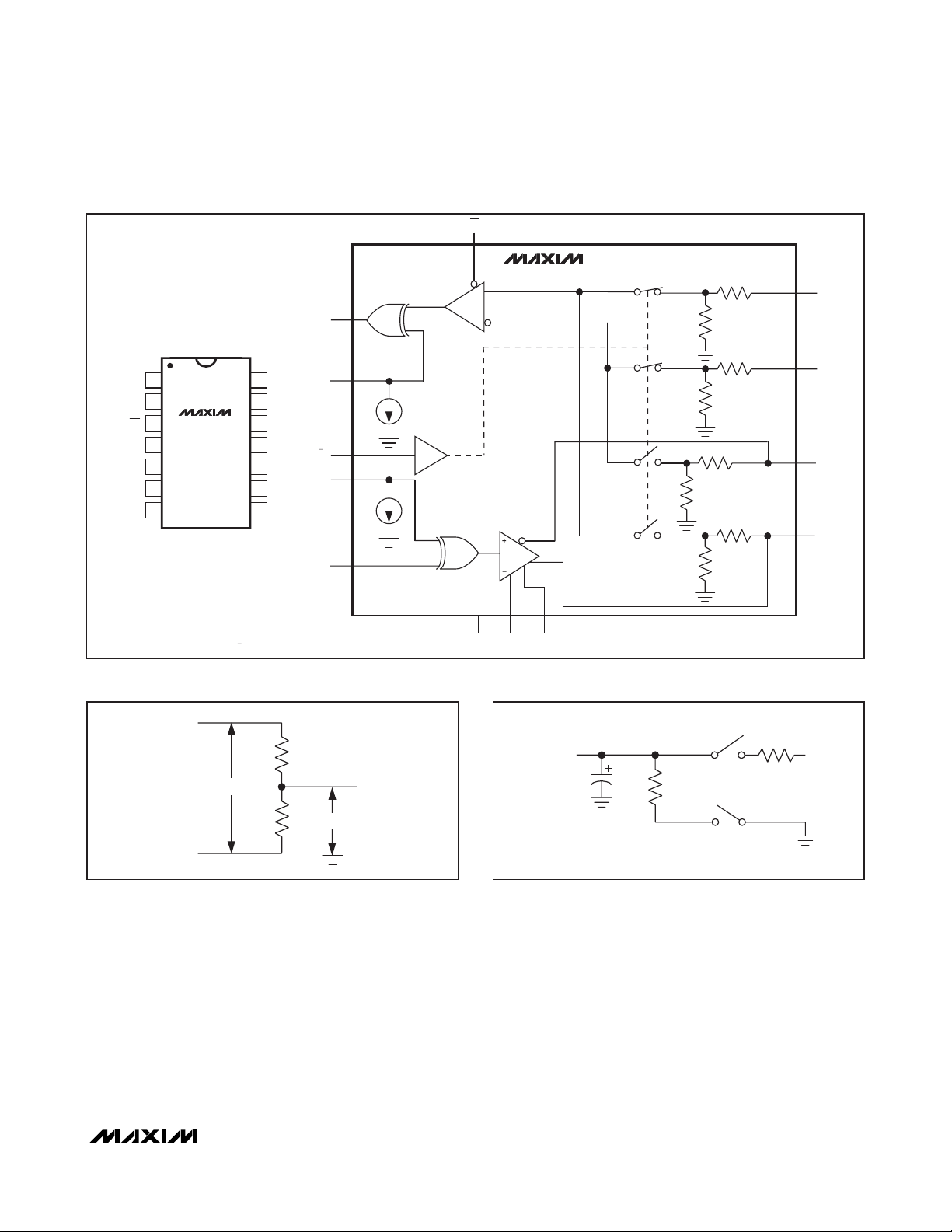
receiver is the same as that of a MAX3080E (Figure 4).
In half-duplex mode, the receiver inputs are switched to
the driver outputs, connecting outputs Y and Z to inputs
A and B, respectively. In half-duplex mode, the internal
full-duplex receiver input resistors are still connected to
pins 11 and 12.
±15kV ESD Protection
As with all Maxim devices, ESD-protection structures
are incorporated on all pins to protect against electrostatic discharges encountered during handling and
assembly. The driver outputs and receiver inputs of the
MAX3080E–MAX3089E family have extra protection
against static electricity. Maxim’s engineers have
developed state-of-the-art structures to protect these
pins against ESD of ±15kV without damage.
±15kV ESD-Protected, Fail-Safe, High-Speed (10Mbps),
Slew-Rate-Limited RS-485/RS-422 Transceivers
14 ______________________________________________________________________________________
Page 15
The ESD-protected pins are tested with reference to the
ground pin in a powered-down condition. They are tested to ±15kV using the Human Body Model.
ESD Test Conditions
ESD performance depends on a variety of conditions.
Contact Maxim for a reliability report that documents
test setup, test methodology, and test results.
Human Body Model
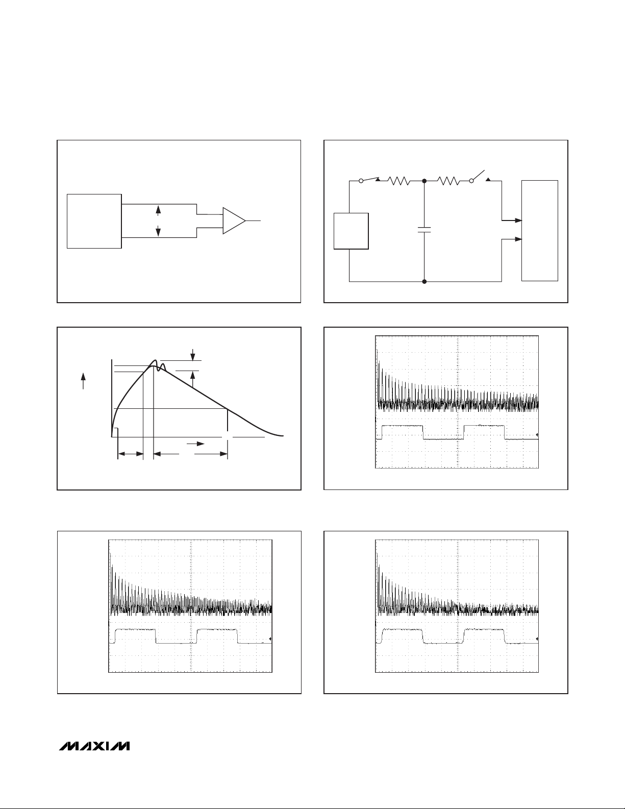
Figure 14a shows the Human Body Model, and Figure
14b shows the current waveform it generates when dis-
charged into a low impedance. This model consists of
a 100pF capacitor charged to the ESD voltage of interest, which is then discharged into the test device
through a 1.5kΩ resistor.
Machine Model
The Machine Model for ESD tests all pins using a
200pF storage capacitor and zero discharge resistance. The objective is to emulate the stress caused
when I/O pins are contacted by handling equipment
during test and assembly. All pins require this protection, not just RS-485 inputs and outputs.
MAX3080E–MAX3089E
±15kV ESD-Protected, Fail-Safe, High-Speed (10Mbps),
Slew-Rate-Limited RS-485/RS-422 Transceivers
______________________________________________________________________________________ 15
Figure 5. Driver DC Test Load
Figure 6. Receiver Enable/Disable Timing Test Load
Figure 4. MAX3089E Pin Configuration and Functional Diagram
TOP VIEW
1
H/F
2
RO
3
RE
4
DE
5
DI
6
SRL
7
GND
NOTE: SWITCH POSITIONS
INDICATED FOR H/F = GND
MAX3089E
DIP/SO
V
RE
CC
MAX3089E
A
RD
14
V
RXP
CC
13
RXP
A
12
B
11
10
9
8
Z
Y
TXP
H/F
TXP
DI
GND DE SRL
B
Z
Y
Y
R
V
OD
R
V
OC
Z
RECEIVER
OUTPUT
TEST POINT
C
RL
15pF
S1
1k
S2
1k
V
CC
Page 16
MAX3080E–MAX3089E
±15kV ESD-Protected, Fail-Safe, High-Speed (10Mbps),
Slew-Rate-Limited RS-485/RS-422 Transceivers
16 ______________________________________________________________________________________
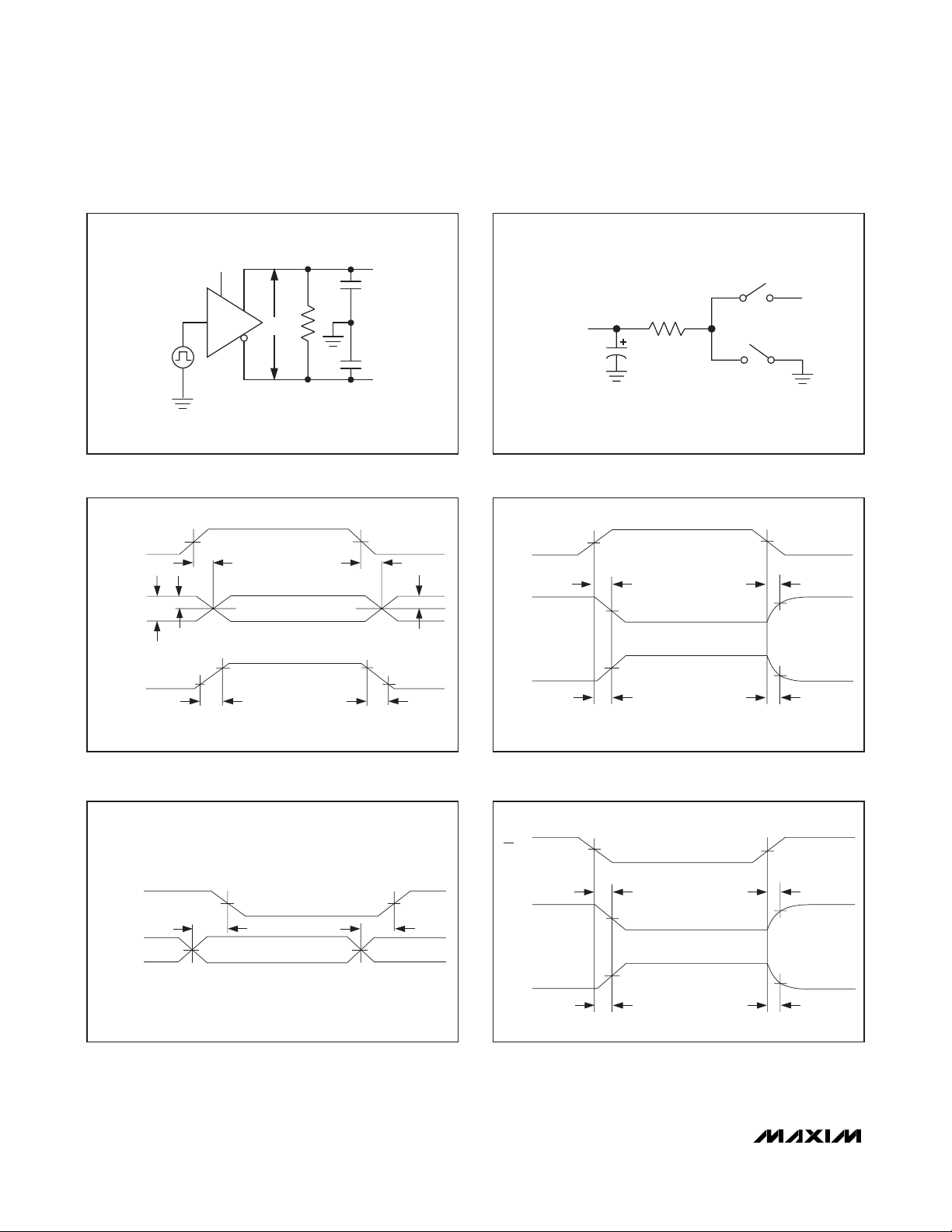
Figure 7. Driver Timing Test Circuit Figure 8. Driver Enable and Disable Timing Test Load
Figure 9. Driver Propagation Delays Figure 10. Driver Enable and Disable Times (Except
MAX3081E/MAX3084E/MAX3087E)
Figure 11. Receiver Propagation Delays Figure 12. Receiver Enable and Disable Times (Except
MAX3081E/MAX3084E/MAX3087E)
3V
DE
DI
Y
V
OD2
Z
C
L1
R
DIFF
OUTPUT
500Ω
S1
V
CC
UNDER TEST
C
C
L2
L
S2
5V
DI
V
DIFF
1.5V
0
t
DPLH
t
DPHL
1.5V
1/2 V
Z
V
O
Y
1/2 V
O
V
O
0
-V
10%
O
t
DR
V
DIFF
90%
t
SKEW = | tDPLH
= V (Y) - V (Z)
- t
DPHL
90%
t
DF
|
10%
O
5V
DE
1.5V 1.5V
0
Y, Z
V
Y, Z
t
, t
DZL(SHDN)
2.3V
OL
OUTPUT NORMALLY LOW
OUTPUT NORMALLY HIGH
0
2.3V
t
DZH(SHDN)
, t
DZL
DZH
t
DLZ
t
DHZ
5V
-1V
RE
V
OH
RO
V
OL
A
1V
B
1.5V 1.5V
t
RPHL
OUTPUT
t
RPLH
INPUT
V
CC
RO
RO
1.5V 1.5V
0
t
, t
RZL(SHDN)
RZL
1.5V
OUTPUT NORMALLY LOW
OUTPUT NORMALLY HIGH
1.5V
0
t
, t
RZH(SHDN)
RZH
t
RLZ
t
RHZ
V
+0.5V
OL
V
-0.5V
OH
VOL + 0.5V
V
- 0.5V
OH
Page 17
MAX3080E–MAX3089E
±15kV ESD-Protected, Fail-Safe, High-Speed (10Mbps),
Slew-Rate-Limited RS-485/RS-422 Transceivers
______________________________________________________________________________________ 17
Figure 13. Receiver Propagation Delay Test Circuit
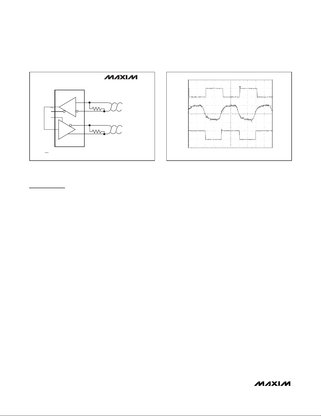
Figure 15. Driver Output Waveform and FFT Plot of
MAX3086E/MAX3087E/MAX3088E, and MAX3089E with
SRL = GND, Transmitting a 20kHz Signal
Figure 14a. Human Body ESD Test Model
Figure 14b. Human Body Current Waveform
Figure 16. Driver Output Waveform and FFT Plot of
MAX3083E/MAX3084E/MAX3085E, and MAX3089E
with SRL = V
CC,
Transmitting a 20kHz Signal
Figure 17. Driver Output Waveform and FFT Plot of
MAX3080E/MAX3081E/MAX3082E, and MAX3089E
with SRL = Unconnected, Transmitting a 20kHz Signal
R
1MΩ
C
R
D
1500Ω
B
ATE
V
ID
R
R
A
PEAK-TO-PEAK RINGING
I
r
(NOT DRAWN TO SCALE)
AMPERES
IP 100%
90%
36.8%
10%
0
0
t
RL
TIME
t
DL
CURRENT WAVEFORM
RECEIVER
OUTPUT
DISCHARGE
RESISTANCE
STORAGE
s
CAPACITOR
HIGH-
VOLTAGE
DC
SOURCE
CHARGE-CURRENT
LIMIT RESISTOR
C
100pF
20dB/div
100kHz/div0Hz 1MHz
DEVICE
UNDER
TEST
MAX3080/3089 FIG-14
20dB/div
100kHz/div0Hz 1MHz
A
MAX3080/3089 FIG-15
B
20dB/div
100kHz/div0Hz 1MHz
A
MAX3080/3089 FIG-16
B
Page 18
MAX3080E–MAX3089E
Applications Information
256 Transceivers on the Bus
The standard RS-485 receiver input impedance is 12kΩ
(one-unit load), and the standard driver can drive up to
32 unit loads. The MAX3080E family of transceivers
have a 1/8-unit-load receiver input impedance (96kΩ),
allowing up to 256 transceivers to be connected in parallel on one communication line. Any combination of
these devices and/or other RS-485 transceivers with a
total of 32 unit loads or less can be connected to the
line.
Reduced EMI and Reflections
The MAX3080E–MAX3085E, and MAX3089E with SRL =
V
CC
or unconnected, are slew-rate limited, minimizing
EMI and reducing reflections caused by improperly terminated cables. Figure 15 shows the driver output
waveform and its Fourier analysis of a 20kHz signal
transmitted by a MAX3086E/MAX3087E/MAX3088E,
and MAX3089E with SRL = GND. High-frequency harmonic components with large amplitudes are evident.
Figure 16 shows the same signal displayed for a
MAX3083E/MAX3084E/MAX3085E, and MAX3089E with
SRL = V
CC, transmitting under the same conditions.
Figure 16’s high-frequency harmonic components are
much lower in amplitude, compared with Figure 15’s,
and the potential for EMI is significantly reduced. Figure
17 shows the same signal displayed for a MAX3080E/
MAX3081E/MAX3082E, and MAX3089E with SRL =
unconnected, transmitting under the same conditions.
Figure 17’s high-frequency harmonic components are
even lower.
In general, a transmitter’s rise time relates directly to the
length of an unterminated stub, which can be driven with
only minor waveform reflections. The following equation
expresses this relationship conservatively:
Length = t
RISE
/ (10 x 1.5ns/ft)
where t
RISE
is the transmitter’s rise time.
For example, the MAX3080E’s rise time is typically
1320ns, which results in excellent waveforms with a stub
length up to 90 feet. A system can work well with longer
unterminated stubs, even with severe reflections, if the
waveform settles out before the UART samples them.
Low-Power Shutdown Mode
(Except MAX3082E/MAX3085E/MAX3088E)
Low-power shutdown mode is initiated by bringing both
RE high and DE low. In shutdown, the devices typically
draw only 1nA of supply current.
RE and DE may be driven simultaneously; the parts are
guaranteed not to enter shutdown if RE is high and DE
is low for less than 50ns. If the inputs are in this state
for at least 600ns, the parts are guaranteed to enter
shutdown.
Enable times tZHand tZLin the
Switching Char-
acteristics
tables assume the part was not in a low-
power shutdown state. Enable times t
ZH(SHDN)
and
t
ZL(SHDN)
assume the parts were shut down. It takes
drivers and receivers longer to become enabled from
low-power shutdown mode (t
ZH(SHDN)
, t
ZL(SHDN)
) than
from driver/receiver-disable mode (tZH, tZL).
±15kV ESD-Protected, Fail-Safe, High-Speed (10Mbps),
Slew-Rate-Limited RS-485/RS-422 Transceivers
18 ______________________________________________________________________________________
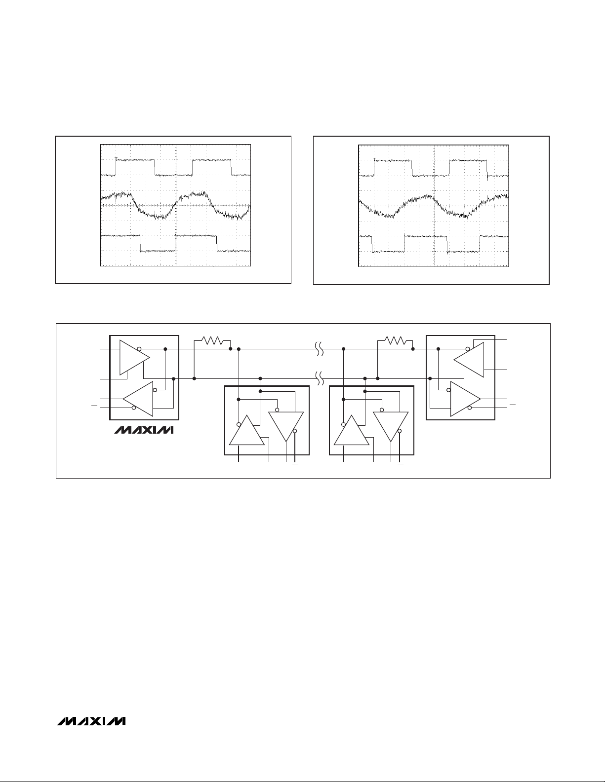
Figure 18. Line Repeater for MAX3080E/MAX3081E/MAX3083E/
MAX3084E/MAX3086E/MAX3087E, and MAX3089E in Full-Duplex
Mode
Figure 19. MAX3080E/MAX3081E/MAX3082E, and MAX3089E
with SRL = Unconnected, System Differential Voltage at 50kHz
Driving 4000ft of Cable
MAX3080/3089 FIG-18
MAX3080E/MAX3081E/MAX3083E/
MAX3084E/MAX3086E/MAX3087E/
MAX3089E (FULL DUPLEX)
A
RO
RE
DE
DI
R
D
120Ω
B
Z
120Ω
Y
DATA IN
DATA OUT
VA - V
DI
B
RO
5V/div
1V/div
5V/div
NOTE: RE AND DE ON MAX3080E/MAX3083E/MAX3086E/MAX3089E ONLY.
5μs/div
Page 19
Driver Output Protection
Two mechanisms prevent excessive output current and
power dissipation caused by faults or by bus contention. The first, a foldback current limit on the output
stage, provides immediate protection against short circuits over the whole common-mode voltage range (see
Typical Operating Characteristics
). The second, a thermal shutdown circuit, forces the driver outputs into a
high-impedance state if the die temperature becomes
excessive.
Line Length vs. Data Rate
The RS-485/RS-422 standard covers line lengths up to
4000 feet. For line lengths greater than 4000 feet, use
the repeater application shown in Figure 18.
Figures 19, 20, and 21 show the system differential voltage for the parts driving 4000 feet of 26AWG twistedpair wire at 110kHz into 120Ω loads.
Typical Applications
The MAX3082E/MAX3085E/MAX3088E/MAX3089E
transceivers are designed for bidirectional data communications on multipoint bus transmission lines.
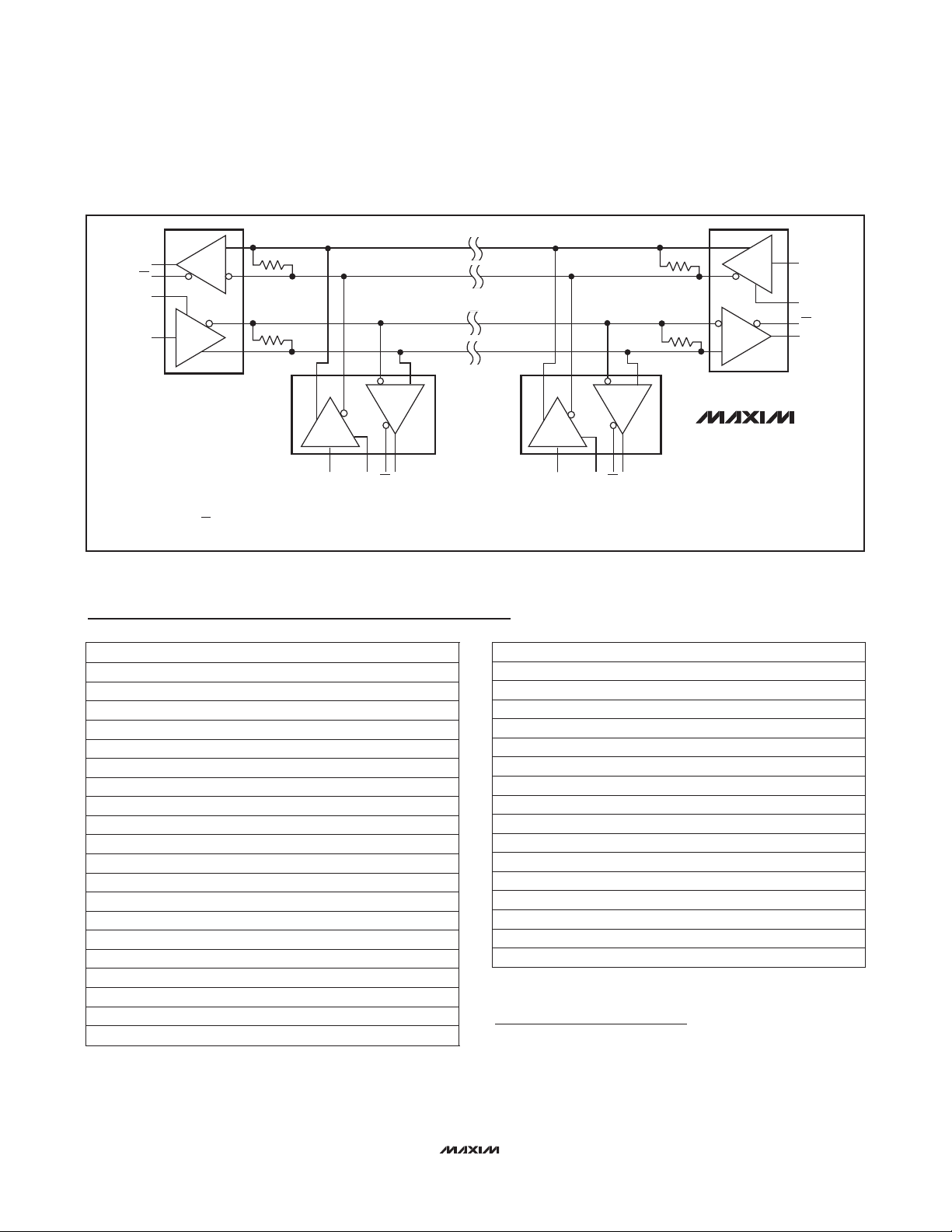
Figures 22 and 23 show typical network applications
circuits. These parts can also be used as line repeaters,
with cable lengths longer than 4000 feet, as shown in
Figure 18.
To minimize reflections, the line should be terminated at
both ends in its characteristic impedance, and stub
lengths off the main line should be kept as short as
possible. The slew-rate-limited MAX3082E/MAX3085E,
and the two modes of the MAX3089E, are more tolerant
of imperfect termination.
MAX3080E–MAX3089E
±15kV ESD-Protected, Fail-Safe, High-Speed (10Mbps),
Slew-Rate-Limited RS-485/RS-422 Transceivers
______________________________________________________________________________________ 19
Figure 20. MAX3083E/MAX3084E/MAX3085E, and MAX3089E
with SRL = V
CC,
System Differential Voltage at 50kHz Driving
4000ft of Cable
Figure 21. MAX3086E/MAX3087E/MAX3088E, and MAX3089E
with SRL = GND, System Differential Voltage at 200kHz Driving
4000ft of Cable
Figure 22. Typical Half-Duplex RS-485 Network
MAX3080/3089 FIG-19
5V/div
1V/div
5V/div
VA - V
DI
B
RO
2μs/div
120Ω
DI
DE
RO
RE
D
R
MAX3082E
MAX3085E
MAX3088E
*MAX3089E (HALF-DUPLEX)
B/Z*
A/Y*
B
A
D
DE
DI RO DE
MAX3080/3089 FIG-20
DI
VA - V
B
RO
1μs/div
120Ω
B
D
B
A
R
D
DI
R
RO
A
R
RERE
5V/div
1V/div
5V/div
DE
DI
RO
RE
Page 20
Maxim cannot assume responsibility for use of any circuitry other than circuitry entirely embodied in a Maxim product. No circuit patent licenses are
implied. Maxim reserves the right to change the circuitry and specifications without notice at any time.
20
__________________Maxim Integrated Products, 120 San Gabriel Drive, Sunnyvale, CA 94086 (408) 737-7600
© 2006 Maxim Integrated Products is a registered trademark of Maxim Integrated Products, Inc.
MAX3080E–MAX3089E
±15kV ESD-Protected, Fail-Safe, High-Speed (10Mbps),
Slew-Rate-Limited RS-485/RS-422 Transceivers
Figure 23. Typical Full-Duplex RS-485 Network
8 Plastic DIP-40°C to +85°CMAX3085EEPA
14 SO-40°C to +85°CMAX3083EESD
14 Plastic DIP0°C to +70°CMAX3083ECPD
14 SO0°C to +70°C
MAX3083ECSD
8 Plastic DIP-40°C to +85°CMAX3082EEPA
8 SO-40°C to +85°CMAX3082EESA
8 Plastic DIP0°C to +70°CMAX3082ECPA
8 SO0°C to +70°C
MAX3082ECSA
8 Plastic DIP-40°C to +85°CMAX3081EEPA
8 SO-40°C to +85°CMAX3081EESA
8 Plastic DIP0°C to +70°CMAX3081ECPA
8 SO0°C to +70°C
MAX3081ECSA
PIN-PACKAGETEMP. RANGEPART
14 Plastic DIP-40°C to +85°CMAX3083EEPD
8 SO0°C to +70°C
MAX3084ECSA
8 Plastic DIP0°C to +70°CMAX3084ECPA
8 SO-40°C to +85°CMAX3084EESA
8 Plastic DIP-40°C to +85°CMAX3084EEPA
8 SO0°C to +70°C
MAX3085ECSA
8 Plastic DIP0°C to +70°CMAX3085ECPA
8 SO-40°C to +85°CMAX3085EESA
Ordering Information (continued)
PART TEMP. RANGE PIN-PACKAGE
MAX3086ECSD
0°C to +70°C 14 SO
MAX3086ECPD 0°C to +70°C 14 Plastic DIP
MAX3086EESD -40°C to +85°C 14 SO
MAX3086EEPD -40°C to +85°C 14 Plastic DIP
MAX3087ECSA
0°C to +70°C 8 SO
8 Plastic DIP0°C to +70°CMAX3087ECPA
MAX3087EESA -40°C to +85°C 8 SO
8 Plastic DIP-40°C to +85°CMAX3087EEPA
MAX3088ECSA
0°C to +70°C 8 SO
8 Plastic DIP0°C to +70°CMAX3088ECPA
MAX3088EESA -40°C to +85°C 8 SO
8 Plastic DIP-40°C to +85°CMAX3088EEPA
MAX3089ECSD
0°C to +70°C 14 SO
14 Plastic DIP0°C to +70°CMAX3089ECPD
MAX3089EESD -40°C to +85°C 14 SO
14 Plastic DIP-40°C to +85°CMAX3089EEPD
Revision History
Pages changed at Rev 1: 1, 19, 20
A
RO
RE
DE
DI
R
D
NOTE: RE AND DE ON MAX3080E/MAX3083E/MAX3086E/MAX3089E ONLY.
120Ω
B
Z
120Ω
Y
Z
Y
D
DI DIRO RO
DE DE
AA
BB
R
RE
Y
120Ω
Z
B
120Ω
Z
Y
R
D
RE
A
MAX3089E (FULL-DUPLEX)
D
R
MAX3080E
MAX3081E
MAX3083E
MAX3084E
MAX3086E
MAX3087E
DI
DE
RE
RO
 Loading...