

Page 1
For free samples & the latest literature: http://www.maxim-ic.com, or phone 1-800-998-8800.
For small orders, phone 1-800-835-8769.
General Description
The MAX2651/MAX2652/MAX2653 silicon germanium
(SiGe), low-noise amplifiers (LNAs) are intended for use
in GSM900, DCS1800, and PCS1900 band wireless
handsets. The MAX2651/MAX2652 consist of two LNAs,
one optimized for the GSM900 band and the other optimized for the DCS1800/PCS1900 bands. They feature a
band-select pin to switch between the two LNAs, as well
as a gain-step input to reduce the gain of each LNA by
20dB and reduce supply current. The MAX2652 is functionally equivalent to the MAX2651, but features a lowpower shutdown mode. The MAX2653 consists of a
single LNA optimized for the DCS1800 and PCS1900
bands, and has a shutdown feature and a 20dB gain
step.
The MAX2652 and MAX2653 together form an ideal
solution for triple-band phone applications (GSM, DCS,
and PCS bands).
The MAX2651/MAX2652/MAX2653 are fabricated using
an advanced high-frequency SiGe bipolar process. As
a result, all devices provide low noise figure, high gain,
and high input third-order intercept point (IP3) performance at the GSM, DCS, and PCS bands. A pull-up
resistor to VCCat each LNA output allows for gain
adjustability. A minimal number of external components
are needed for input and output matching, helping to
reduce board space.
The MAX2651/MAX2652 are packaged in a 10-pin µMAX,
while the MAX2653 is packaged in an 8-pin µMAX. All
devices operate from a single +2.7V to +3.3V supply.
Applications
GSM900/DCS1800 Dual-Band Phones
GSM900/DCS1800/PCS1900 Triple-Band Phones
DCS1800 or PCS1900 Single-Mode Phones
IS-136 TDMA Dual-Band Phones
Features
♦ Wide Operating Frequency Range
800MHz to 1000MHz (MAX2651/52)
1800MHz to 2000MHz (MAX2651/52/53)
♦ Excellent Low-Noise Performance
1.2dB/1.3dB over GSM Receive Band
(MAX2651/52)
1.8dB/1.8dB/1.7dB over DCS Receive Band
(MAX2651/52/53)
♦ High Gain
18dB over GSM Receive Band (MAX2651/52)
18dB/17.5dB/18.5dB over DCS Receive Band
(MAX2651/52/53)
♦ 20dB Gain Reduction in Low-Gain Mode
♦ Externally Adjustable Gain
♦ +2.7V to +3.3V Single-Supply Operation
♦ Low Supply Current
5.4mA to 7.0mA in High-Gain Mode
2.2mA in Low-Gain Mode
♦ 0.25µA Shutdown Current (MAX2652/53)
MAX2651/MAX2652/MAX2653
GSM900 and DCS1800/PCS1900
Dual-Band, Low-Noise Amplifiers
________________________________________________________________ Maxim Integrated Products 1
19-1506; Rev 1; 10/99
PART
MAX2651EUB
MAX2652EUB
-40°C to +85°C
-40°C to +85°C
TEMP. RANGE PIN-PACKAGE
10 µMAX
10 µMAX
Pin Configurations/Functional Diagrams
Ordering Information
10
9
8
7
6
1
2
3
4
5
SHDN (GND) GAIN
GSMOUT
V
CC
DCSOUT
GND
GND
DCSIN
BAND
GSMIN
DC BIAS
CONTROL
MAX2651
MAX2652
HIGH
LOW
LOW
HIGH
8
7
6
5
1
2
3
4
SHDN GAIN
V
CC
DCSOUT
GND
DCSIN
GND
GND
HIGH
LOW
MAX2653
DC BIAS
CONTROL
MAX2653EUA
-40°C to +85°C 8 µMAX
( ) ARE FOR MAX2651.
Page 2
MAX2651/MAX2652/MAX2653
GSM900 and DCS1800/PCS1900
Dual-Band, Low-Noise Amplifiers
2 _______________________________________________________________________________________
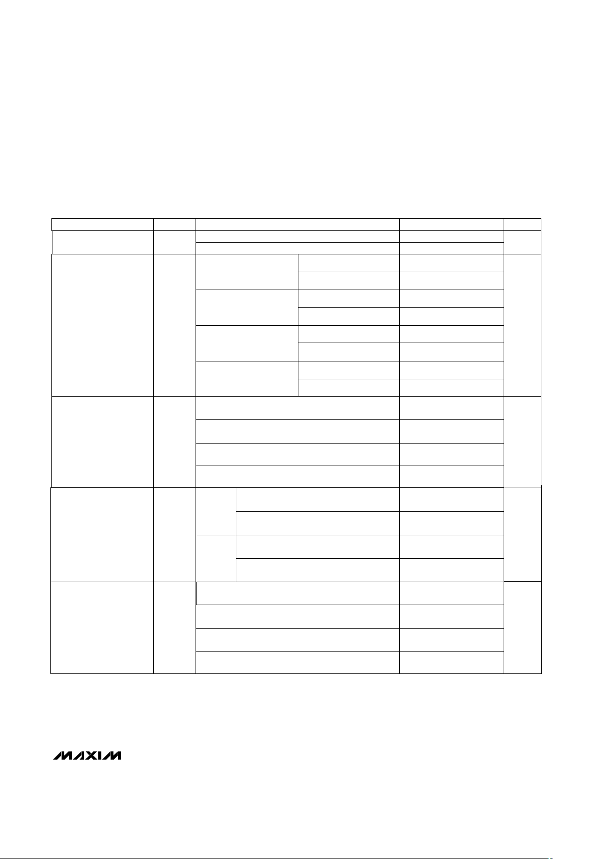
ABSOLUTE MAXIMUM RATINGS
DC ELECTRICAL CHARACTERISTICS—MAX2651
(VCC= +2.7V to +3.3V, BAND = GAIN = VCC, no input signal, all input/output ports terminated in 50Ω, TA= -40°C to +85°C, unless
otherwise noted. Typical values are at V
CC
= +3V, TA= +25°C.) (Note 1)
Stresses beyond those listed under “Absolute Maximum Ratings” may cause permanent damage to the device. These are stress ratings only, and functional
operation of the device at these or any other conditions beyond those indicated in the operational sections of the specifications is not implied. Exposure to
absolute maximum rating conditions for extended periods may affect device reliability.
VCCto GND..............................................................-0.3V to +6V
SHDN, GAIN, BAND to GND......................-0.3V to (V
CC
+ 0.3V)
GSMIN, DCSIN ..........................................1.0V peak (+10dBm)
Input Current (all digital inputs) .......................................±10mA
Continuous Power Dissipation
8-Pin µMAX (derate 4.5mW/°C above +70°C)..............362mW
10-Pin µMAX (derate 5.6mW/°C above +70°C) ............444mW
Operating Temperature Range ...........................-40°C to +85°C
Junction Temperature......................................................+150°C
Storage Temperature Range .............................-65°C to +150°C
Lead Temperature (soldering, 10sec) .............................+300°C
DCS band, low-gain mode
(BAND = VCC, GAIN = GND)
DCS band, high-gain mode
(BAND = GAIN = VCC)
VIN= GND
VIN= V
CC
GSM band, high-gain mode
(BAND = GND, GAIN = VCC)
GSM band, low-gain mode
(BAND = GND, GAIN = VCC)
CONDITIONS
2.2 3.3
5.7 8.7
I
CC
V
2.7 3.3
V
CC
Input Voltage Range
Input Supply Current
µA
-1.5
I
IL
Input Logic Low Current
µA
1.5
I
IH
Input Logic High Current
5.9 9.6
2.2 3.6
V1.5V
IH
Input Logic Threshold High
V
0.5
V
IL
Input Logic Threshold Low
UNITSMIN TYP MAXSYMBOLPARAMETER
mA
DCS band, low-gain mode
(BAND = V
CC
, GAIN = GND)
DCS band, high-gain mode
(BAND = GAIN = VCC)
VIN= GND
VIN= V
CC
GSM band, high-gain mode
(BAND = GND, GAIN = VCC)
GSM band, low-gain mode
(BAND = GND, GAIN = VCC)
CONDITIONS
mA
2.3 3.6
7.0 11.0
I
CC
V
2.7 3.3
V
CC
Input Voltage Range
Input Supply Current
µA
-1.5
I
IL
Input Logic Low Current
µA
1.5
I
IH
Input Logic High Current
7.2 11.0
2.4 3.7
V1.5V
IH
Input Logic Threshold High
V
0.5
V
IL
Input Logic Threshold Low
UNITSMIN TYP MAXSYMBOLPARAMETER
DC ELECTRICAL CHARACTERISTICS—MAX2652
(VCC= +2.7V to +3.3V, BAND = GAIN = VCC, no input signal, all input/output ports terminated in 50Ω, TA= -40°C to +85°C, unless
otherwise noted. Typical values are at V
CC
= +3V, TA= +25°C.) (Note 1)
SHDN = GND
µA0.25Shutdown Supply Current
Page 3
MAX2651/MAX2652/MAX2653
GSM900 and DCS1800/PCS1900
Dual-Band, Low-Noise Amplifiers
_______________________________________________________________________________________ 3
DC ELECTRICAL CHARACTERISTICS—MAX2653
(VCC= +2.7V to +3.3V, SHDN = GAIN = VCC, no input signal, all input/output ports terminated in 50Ω, TA= -40°C to +85°C, unless
otherwise noted. Typical values are at V
CC
= +3V, TA= +25°C.) (Note 1)
DCS band, low-gain mode (GAIN = GND)
DCS band, high-gain mode (GAIN = VCC)
VIN= V
CC
VIN= GND
CONDITIONS
2.2 3.2
mA
5.4 8.5
I
CC
V
2.7 3.3
V
CC
Input Voltage Range
Input Supply Current
V
1.5
V
IH
Input Logic Threshold High
V
0.5
V
IL
Input Logic Threshold Low
µA
3
I
IH
Input Logic High Current
µA
-1.5
I
IL
Input Logic Low Current
UNITSMIN TYP MAXSYMBOLPARAMETER
Note 1: Devices are production tested at TA= +25°C. Minimum and maximum limits are guaranteed by design and characterization.
SHDN = GND
µA
0.25
I
SHDN
Shutdown Supply Current
AC ELECTRICAL CHARACTERISTICS—MAX2651
(MAX2651 EV kit, f
IN
= 945MHz (GSM band), fIN= 1850MHz (DCS band), PIN= -30dBm, input and output matching networks are
optimized for the frequency band of interest, all input/output ports terminated in 50Ω, V
CC
= +3V, TA= +25°C, unless otherwise noted.)
(Note 2)
-4 0
16 20
-4 0
16 20
TA= -40°C to +85°C
TA= -40°C to +85°C
TA= -40°C to +85°C
TA= +25°C
TA= +25°C
TA= +25°C
TA= +25°C
MIN TYP MAX UNITS
Noise Figure (Note 4)
1.8 2.05
-3.5 -2 -0.5
16.5 18 19.5
-3.5 -2 -0.5
5.5 6.0
1.2 1.4
5.3 6.7
Input Frequency Range
(Note 3)
f
IN
1805 1880
925 960
Power Gain (Note 4)
16.5 18 19.5
CONDITIONS
DCS band, high-gain mode
(BAND = GAIN = V
CC
)
DCS band, low-gain
mode (BAND = VCC,
GAIN = GND)
DCS band, low-gain mode
(BAND = VCC, GAIN = GND)
GSM band, high-gain mode
(BAND = GND, GAIN = VCC)
GSM band, low-gain mode
(BAND = GAIN = GND)
DCS band (BAND = VCC)
GSM band (BAND = GND)
DCS band, high-gain
mode (BAND = GAIN =
V
CC
)
GSM band, high-gain
mode (BAND = GND,
GAIN = V
CC
)
TA= -40°C to +85°C
GSM band, low-gain
mode (BAND = GAIN =
GND)
MHz
dB
dB
NF
G
PARAMETER SYMBOL
Page 4
MAX2651/MAX2652/MAX2653
GSM900 and DCS1800/PCS1900
Dual-Band, Low-Noise Amplifiers
4 _______________________________________________________________________________________
AC ELECTRICAL CHARACTERISTICS—MAX2651 (continued)
(MAX2651 EV kit, f
IN
= 945MHz (GSM band), fIN= 1850MHz (DCS band), PIN= -30dBm, input and output matching networks are
optimized for the frequency band of interest, all input/output ports terminated in 50Ω, V
CC
= +3V, TA= +25°C, unless otherwise noted.)
(Note 2)
GSM band, high-gain mode
(BAND = GND, GAIN = VCC)
DCS band, low-gain mode
(BAND = VCC, GAIN = GND)
DCS band, high-gain mode
(BAND = GAIN = V
CC
)
GSM band, low-gain mode
(BAND = GAIN = GND)
GSM band, high-gain mode
(BAND = GND, GAIN = VCC)
DCS band, low-gain mode
(BAND = V
CC
, GAIN = GND)
DCS band, high-gain mode
(BAND = GAIN = V
CC
)
Reverse Isolation
-19 -15
-12 -10
dB
-14 -10
S
22
2
Output Return Loss
-20 -15
-11 -8.5
-14 -12
dB
-11 -8.5
S
11
2
Input Return Loss
GSM band, low-gain mode
(BAND = GAIN = GND)
GSM band, high-gain mode
(BAND = GND, GAIN = VCC)
DCS band, low-gain mode
(BAND = V
CC
, GAIN = GND)
DCS band, high-gain mode
(BAND = GAIN = V
CC
)
GSM band, low-gain mode
(BAND = GAIN = GND)
-22 -20
-39 -35
-20 -18
dB
-32 -29
S
12
2
-20 -15
GSM band, low-gain mode
(BAND = GND, GAIN = GND)
GSM band, high-gain mode
(BAND = GND, GAIN = VCC)
(Note 5)
DCS band, low-gain mode
(BAND = VCC, GAIN = GND)
-10.5 -8.5
-20 -18
-9.5 -8
dBmIP
-1dB
Input 1dB Compression Point
dBm
-11.5 -10
IIP3Input Third-Order Intercept Point
DCS band, high-gain mode
(BAND = GAIN = VCC)
DCS band, high-gain mode
(BAND = GAIN = VCC)
-1.5 0.5
DCS band, low-gain mode
(BAND = VCC, GAIN = GND)
(Note 6)
-10.5 -8.5
-2.5 0.5
GSM band, high-gain mode
(BAND = GND, GAIN = VCC)
GSM band, low-gain mode
(BAND = GND, GAIN = GND)
CONDITIONS UNITSMIN TYP MAXSYMBOLPARAMETER
-20 -18
Page 5
MAX2651/MAX2652/MAX2653
GSM900 and DCS1800/PCS1900
Dual-Band, Low-Noise Amplifiers
_______________________________________________________________________________________ 5
AC ELECTRICAL CHARACTERISTICS—MAX2652
(MAX2652 EV kit, f
IN
= 945MHz (GSM band), fIN= 1850MHz (DCS band), PIN= -30dBm, input and output matching networks are
optimized for the frequency band of interest, all input/output ports terminated in 50Ω, V
CC
= +3V, TA= +25°C, unless otherwise noted.)
(Note 2)
1805 1880
925 960
16 17.5 19
15.5 19.5
-3.5 -2 -0.5
-4 0
16.5 18 19.5
16 20
-4.0 -2 -0.5
1.3 1.5
1.8 2.0
5.8 6.3
5.5 6.7
-10 -8.5
IIP3
Input Third-Order
Intercept Point
IP
-1dB
Input 1dB Compression
Point
(Note 6)
(Note 5)
SYMBOL
TA= -40°C to +85°C
DCS band, high-gain mode
(BAND = GAIN = VCC)
GSM band, high-gain mode
(BAND = GND, GAIN = VCC)
DCS band, high-gain mode
(BAND = GAIN = V
CC
)
DCS band, high-gain mode
(BAND = GAIN = V
CC
)
f
IN
G
DCS band, low-gain mode
(BAND = VCC, GAIN = GND)
-18 -16.5
GSM band (BAND = GND)
GSM band, low-gain mode
(BAND = GND, GAIN = GND)
GSM band, high-gain mode
(BAND = GND, GAIN = V
CC
)
DCS band, low-gain mode
(BAND = VCC, GAIN = GND)
-18 -16.5
-10.5 -8
-8.5 -7
0 1.5
DCS band, low-gain mode
(BAND = VCC, GAIN = GND)
-9 -7.5
0.5 2.5
GSM band, high-gain mode
(BAND = GND, GAIN = VCC)
GSM band, low-gain mode
(BAND = GND, GAIN = GND)
DCS band (BAND = VCC)
GSM band, low-gain mode
(BAND = GAIN = GND)
DCS band, low-gain
mode (BAND = V
CC
,
GAIN = GND)
GSM band, high-gain
mode (BAND = GND,
GAIN = VCC)
GSM band, low-gain
mode (BAND = GAIN =
GND)
CONDITIONS
Power Gain (Note 4)
Input Frequency Range
(Note 3)
NFNoise Figure (Note 4)
MIN TYP MAX
TA= +25°C
TA= +25°C
TA= +25°C
TA= +25°C
TA= -40°C to +85°C
TA= -40°C to +85°C
TA= -40°C to +85°C
PARAMETER
DCS band, high-gain
mode (BAND = GAIN =
V
CC
)
-4.5 0
MHz
dBm
dBm
dB
dB
UNITS
Page 6

MAX2651/MAX2652/MAX2653
GSM900 and DCS1800/PCS1900
Dual-Band, Low-Noise Amplifiers
6 _______________________________________________________________________________________
AC ELECTRICAL CHARACTERISTICS—MAX2652 (continued)
(MAX2652 EV kit, f
IN
= 945MHz (GSM band), fIN= 1850MHz (DCS band), PIN= -30dBm, input and output matching networks are
optimized for the frequency band of interest, all input/output ports terminated in 50Ω, V
CC
= +3V, TA= +25°C, unless otherwise noted.)
(Note 2)
Input Return Loss
Reverse Isolation
S
12
2
GSM band, high-gain mode
(BAND = GND, GAIN = VCC)
DCS band, low-gain mode
(BAND = VCC, GAIN = GND)
DCS band, high-gain mode
(BAND = GAIN = VCC)
GSM band, high-gain mode
(BAND = GND, GAIN = VCC)
DCS band, low-gain mode
(BAND = V
CC
, GAIN = GND)
DCS band, high-gain mode
(BAND = GAIN = V
CC
)
GSM band, low-gain mode
(BAND = GAIN = GND)
GSM band, high-gain mode
(BAND = GND, GAIN = V
CC
)
DCS band, low-gain mode
(BAND = VCC, GAIN = GND)
DCS band, high-gain mode
(BAND = GAIN = VCC)
CONDITIONSSYMBOLPARAMETER
GSM band, low-gain mode
(BAND = GAIN = GND)
S
11
2
S
22
2
Output Return Loss
GSM band, low-gain mode
(BAND = GAIN = GND)
dB
dB
dB
UNIT
MIN TYP MAX
-12 -9.5
-12 -9.5
-11 -9.5
-20 -15
-11 -9.5
-17 -13
-12.5 -11
-15 -13
-29 -26
-19 -17
-37 -34
-23 -20
Page 7

MAX2651/MAX2652/MAX2653
GSM900 and DCS1800/PCS1900
Dual-Band, Low-Noise Amplifiers
_______________________________________________________________________________________ 7
AC ELECTRICAL CHARACTERISTICS—MAX2653
(MAX2653 EV kit, fIN= 1850MHz (DCS band), fIN= 1960MHz (PCS band), PIN= -30dBm, input and output matching networks are
optimized for the frequency band of interest, all input/output ports terminated in 50Ω, V
CC
= +3V, TA= +25°C, unless otherwise
noted.) (Note 2)
Note 2: Minimum and maximum limits are guaranteed by design and characterization, but not production tested.
Note 3: The part has been fully characterized at the specified frequency range. Operation outside of this range is possible but not
guaranteed.
Note 4: Specification excludes circuit board losses.
Note 5: Measured with two tones, f
IN1
= 1850MHz, f
IN2
= 1850.8MHz, PIN= -33dBm for each tone.
Note 6: Measured with two tones, f
IN1
= 945MHz, f
IN2
= 945.8MHz, PIN= -33dBm for each tone.
Note 7: Measured with two tones, f
IN1
= 1960MHz, f
IN2
= 1960.8MHz, PIN= -33dBm for each tone.
PCS band
DCS band
PCS band
DCS band
1.8 2.05
-4 0
16 20
1930 1990
-21 -18
-33 -29
PCS band
DCS band
PCS band
DCS band
DCS and PCS band, low-gain mode
(BAND = VCC, GAIN = GND)
High-gain mode (BAND
= GAIN = V
CC
)
Reverse Isolation
S
12
2
-35 -31
dB
-21 -18
Low-gain mode (BAND =
VCC, GAIN = GND)
DCS and PCS band, high-gain mode
(BAND = GAIN = V
CC
)
Output Return Loss
S
22
2
-12 -9.5
dB
-15 -12
DCS and PCS band, low-gain mode
(BAND = V
CC
, GAIN = GND)
DCS and PCS band, high-gain mode
(BAND = GAIN = VCC)
Input Return Loss
S
11
2
-11 -8.5
dB
-11 -9.5
DCS and PCS band, low-gain mode
(BAND = VCC, GAIN = GND)
-1 +1.5
DCS and PCS band, high-gain mode
(BAND = GAIN = VCC)
PARAMETER SYMBOL MIN TYP MAX UNITS
Noise Figure (Note 4) NF
1.7 1.9
-4 -2.5 -1
17 18.5 20
5.3 6.7
dB
Input Third-Order
Intercept Point
(Notes 5, 7)
IIP3
-10.5 -8.5
dBm
Input Frequency Range
(Note 3)
f
IN
1805 1880
MHz
Power Gain (Note 4) G dB
Input 1dB Compression
Point
IP
-1dB
-20 -18
dB
-9 -7
CONDITIONS
High-gain mode
(BAND = GAIN = V
CC
)
DCS and PCS band,
low-gain mode (BAND =
V
CC
, GAIN = GND)
DCS and PCS band,
high-gain mode
(BAND = GAIN = VCC)
DCS and PCS band, low-gain mode
(BAND = VCC, GAIN = GND)
DCS and PCS band, low-gain mode
(BAND = V
CC
, GAIN = GND)
DCS and PCS band, high-gain mode
(BAND = V
CC
, GAIN = GND)
BAND = V
CC
TA= +25°C
TA= +25°C
TA= -40°C to +85°C
TA= -40°C to +85°C
Page 8

MAX2651/MAX2652/MAX2653
GSM900 and DCS1800/PCS1900
Dual-Band, Low-Noise Amplifiers
8 _______________________________________________________________________________________
Typical Operating Characteristics
(MAX2651 EV kit, VCC= +3.0V, input and output matched with recommended matching networks, TA= +25°C, unless otherwise noted.)
HIGH GAIN
LOW GAIN
fIN = 945MHz
P
IN
(dBm)
12
10
-9
-11
14
-7
16
-5
18
-3
20
-1
-25 -20 -15 -10 -5 0
POWER GAIN vs. INPUT POWER
MA\X2651-01
POWER GAIN (dB)
LOW GAIN (dB)
-20
-10
0
10
20
800 840 880 920 960 1000
POWER GAIN vs. FREQUENCY
MA\X2651-02
FREQUENCY (MHz)
GAIN (dB)
HIGH GAIN
LOW GAIN
800 840 880 920 960 1000
INPUT RETURN LOSS
vs. FREQUENCY
MA\X2651-03
FREQUENCY (MHz)
S
11
2
(dB)
HIGH GAIN
LOW GAIN
-25
-20
-10
-15
-5
0
800 840 880 920 960 1000
OUTPUT RETURN LOSS
vs. FREQUENCY
MA\X2651-04
FREQUENCY (MHz)
S
22
2
(dB)
HIGH GAIN
-25
-20
-10
-15
-5
0
LOW GAIN
800 840 880 920 960 1000
REVERSE ISOLATION vs. FREQUENCY
MA\X2651-05
FREQUENCY (MHz)
S
12
2
(dB)
-40
-20
-30
-10
0
LOW GAIN
HIGH GAIN
4
5
6
7
8
SUPPLY CURRENT vs. VCC HIGH GAIN
MAX2651-06
VCC (V)
I
CC
(mA)
2.7 3.02.8 2.9 3.1 3.2 3.3
NO INPUT SIGNAL
TA = +25°C
TA = -40°C
TA = +85°C
1.0
1.5
2.0
2.5
3.0
SUPPLY CURRENT vs. VCC LOW GAIN
MAX2651-07
VCC (V)
I
CC
(mA)
2.7 3.02.8 2.9 3.1 3.2 3.3
NO INPUT SIGNAL
TA = +25°C
TA = -40°C
TA = +85°C
MAX2651 (GSM Band)
Page 9

MAX2651/MAX2652/MAX2653
GSM900 and DCS1800/PCS1900
Dual-Band, Low-Noise Amplifiers
_______________________________________________________________________________________ 9
Typical Operating Characteristics (continued)
(MAX2651 EV kit, VCC= +3.0V, input and output matched with recommended matching networks, TA= +25°C, unless otherwise noted.)
HIGH GAIN
LOW GAIN
f = 1840MHz
PIN (dBm)
11
9
-8
-10
13
-6
15
-4
17
-2
19
0
-25 -20 -15 -10 -5 0
POWER GAIN vs. INPUT POWER
MA\X2651-08
POWER GAIN (dB)
LOW GAIN (dB)
-20
-10
0
10
20
1800 1840 1880 1920 1960 2000
POWER GAIN vs. FREQUENCY
MA\X2651-09
FREQUENCY (MHz)
S
21
2
(dB)
HIGH GAIN
LOW GAIN
HIGH GAIN
LOW GAIN
1800 1840 1880 1920 1960 2000
INPUT RETURN LOSS
vs. FREQUENCY
MA\X2651-10
FREQUENCY (MHz)
S
11
2
(dB)
-20
-10
0
1800 1840 1880 1920 1960 2000
OUTPUT RETURN LOSS
vs. FREQUENCY
MA\X2651-11
FREQUENCY (MHz)
S
22
2
(dB)
-20
-10
0
HIGH GAIN
LOW GAIN
1800 1840 1880 1920 1960 2000
REVERSE ISOLATION vs. FREQUENCY
MA\X2651-12
FREQUENCY (MHz)
S
12
2
(dB)
HIGH GAIN
LOW GAIN
-40
-30
-20
-10
0
4
5
6
7
8
SUPPLY CURRENT vs. VCC HIGH GAIN
MAX2651-13
VCC (V)
I
CC
(mA)
2.7 3.02.8 2.9 3.1 3.2 3.3
NO INPUT SIGNAL
TA = +85°C
TA = -40°C
TA = +25°C
1.0
1.5
2.0
2.5
3.0
SUPPLY CURRENT vs. VCC LOW GAIN
MAX2651-14
VCC (V)
I
CC
(mA)
2.7 3.02.8 2.9 3.1 3.2 3.3
NO INPUT SIGNAL
TA = +25°C
TA = -40°C
TA = +85°C
MAX2651 (DCS Band)
Page 10

MAX2651/MAX2652/MAX2653
GSM900 and DCS1800/PCS1900
Dual-Band, Low-Noise Amplifiers
10 ______________________________________________________________________________________
HIGH GAIN
LOW GAIN
f = 945MHz
P
IN
(dBm)
12
10
8
-10
-12
-14
14
-8
16
-6
18
-4
20
-2
-25 -20 -15 -10 -5 0
POWER GAIN vs. INPUT POWER
MA\X2652-01
HIGH GAIN (dB)
LOW GAIN (dB)
5.0
6.0
7.0
8.0
5.5
6.5
7.5
8.5
9.0
HIGH-GAIN MODE
SUPPLY CURRENT vs. SUPPLY VOLTAGE
MAX2652-toc02
SUPPLY VOLTAGE (V)
I
CC
(mA)
2.7 3.02.8 2.9 3.1 3.2 3.3
NO INPUT SIGNAL
TA = -40°C
TA = +25°C
TA = +85°C
1.5
1.0
2.0
2.5
3.0
3.5
LOW-GAIN MODE
SUPPLY CURRENT vs. SUPPLY VOLTAGE
MAX2652 toc03
SUPPLY VOLTAGE (V)
I
CC
(mA)
2.7 3.02.8 2.9 3.1 3.2 3.3
NO INPUT SIGNAL
TA = +25°C
TA = -40°C
TA = +85°C
-3
-5
-7
-9
-11
-1
1
3
5
INPUT IP3 vs. SUPPLY VOLTAGE
MAX2652 toc03a
SUPPLY VOLTAGE (V)
INPUT IP3 (dBm)
2.7 3.02.8 2.9 3.1 3.2 3.3
LOW GAIN
HIGH GAIN
TA = +25°C
TA = +25°C
TA = -40°C
TA = +85°C
TA = -40°C
TA = +85°C
-14
-16
-18
-20
-12
-10
-8
-6
INPUT P1dB vs. SUPPLY VOLTAGE
MAX2652 toc03b
SUPPLY VOLTAGE (V)
INPUT P1dB (dBm)
2.7 3.02.8 2.9 3.1 3.2 3.3
LOW GAIN
HIGH GAIN
TA = +25°C
TA = -40°C
TA = -40°C
TA = +85°C
TA = +85°C
TA = +25°C
-20
-10
0
10
20
800 840 880 920 960 1000
POWER GAIN vs. FREQUENCY
MA\X2652-tocA
FREQUENCY (MHz)
GAIN (dB)
HIGH GAIN
LOW GAIN
800 840 880 920 960 1000
OUTPUT RETURN LOSS
vs. FREQUENCY
MA\X2652-tocC
FREQUENCY (MHz)
S
22
2
(dB)
-50
-40
-20
-30
-10
0
HIGH GAIN
LOW GAIN
800 840 880 920 960 1000
INPUT RETURN LOSS
vs. FREQUENCY
MA\X2652-tocB
FREQUENCY (MHz)
S
11
2
(dB)
LOW GAIN
-50
-40
-20
-30
-10
0
HIGH GAIN
800 840 880 920 960 1000
REVERSE ISOLATION vs. FREQUENCY
MA\X2652-tocD
FREQUENCY (MHz
)
S
12
2
(dB)
-40
-50
-20
-30
-10
0
LOW GAIN
HIGH GAIN
Typical Operating Characteristics (continued)
(MAX2652 EV kit, VCC= +3.0V, input and output matched with recommended matching networks, TA= +25°C, unless otherwise noted.)
MAX2652 (GSM Band)
Page 11

MAX2651/MAX2652/MAX2653
GSM900 and DCS1800/PCS1900
Dual-Band, Low-Noise Amplifiers
______________________________________________________________________________________ 11
HIGH GAIN
LOW GAIN
f = 945MHz
P
IN
(dBm)
12
10
8
-8
-10
-12
14
-6
16
-4
18
-2
20
0
-25 -20 -15 -10 -5 0
POWER GAIN vs. INPUT POWER
MA\X2652-toc04
HIGH GAIN (dB)
LOW GAIN (dB)
-20
-10
0
10
20
1800 1840 1880 1920 1960 2000
POWER GAIN vs. FREQUENCY
MA\X2652 toc05
FREQUENCY (MHz)
GAIN (dB)
HIGH GAIN
LOW GAIN
-40
-50
-30
-20
-10
0
1800 1840 1880 1920
FREQUENCY (MHz)
1960 2000
INPUT RETURN LOSS vs. FREQUENCY
MA\X2652 toc06
S
11
2
(dB)
LOW GAIN
HIGH GAIN
-40
-50
-30
-20
-10
0
1800 1840 1880 1920 1960 2000
OUTPUT RETURN LOSS vs. FREQUENCY
MA\X2652 toc07
HIGH GAIN
LOW GAIN
FREQUENCY (MHz)
S
22
2
(dB)
-40
-50
-30
-20
-10
0
1800 1840 1880 1920 1960 2000
REVERSE ISOLATION vs. FREQUENCY
MA\X2652 toc08
HIGH GAIN
LOW GAIN
FREQUENCY (MHz)
S
12
2
(dB)
5.0
6.0
7.0
8.0
5.5
6.5
7.5
8.5
9.0
HIGH-GAIN SUPPLY CURRENT
vs. SUPPLY VOLTAGE
MAX2652-toc09
SUPPLY VOLTAGE (V)
I
CC
(mA)
2.7 3.02.8 2.9 3.1 3.2 3.3
NO INPUT SIGNAL
TA = -40°C
TA = +25°C
TA = +85°C
1.5
1.0
2.0
2.5
3.0
LOW-GAIN SUPPLY CURRENT
vs. SUPPLY VOLTAGE
MAX2652 toc10
SUPPLY VOLTAGE (V)
I
CC
(mA)
2.7 3.02.8 2.9 3.1 3.2 3.3
NO INPUT SIGNAL
TA = +25°C
TA = -40°C
TA = +85°C
-4
-6
-8
-10
-2
0
2
4
INPUT IP3 vs. SUPPLY VOLTAGE
MAX2652 toc10a
SUPPLY VOLTAGE (V)
INPUT IP3 (dBm)
2.7 3.02.8 2.9 3.1 3.2 3.3
LOW GAIN
HIGH GAIN
TA = +25°C
TA = -40°C
TA = -40°C
TA = +85°C
TA = +85°C
TA = +25°C
-16
-18
-14
-8
-6
-4
INPUT P1dB vs. SUPPLY VOLTAGE
MAX2652 toc10b
SUPPLY VOLTAGE (V)
INPUT 1dB (dBm)
2.7 3.02.8 2.9 3.1 3.2 3.3
LOW GAIN
HIGH GAIN
TA = +25°C
TA = -40°C
TA = -40°C
TA = +85°C
TA = +85°C
TA = +25°C
Typical Operating Characteristics (continued)
(MAX2652 EV kit, VCC= +3.0V, input and output matched with recommended matching networks, TA= +25°C, unless otherwise noted.)
MAX2652 (DCS Band)
Page 12

MAX2651/MAX2652/MAX2653
GSM900 and DCS1800/PCS1900
Dual-Band, Low-Noise Amplifiers
12 ______________________________________________________________________________________
Typical Operating Characteristics (continued)
(MAX2653 EV kit, VCC= +3.0V, input and output matched with recommended matching networks, TA= +25°C, unless otherwise noted.)
HIGH GAIN
LOW GAIN
f = 1840MHz
10
-11
12
-9
14
-7
16
-5
18
-3
-25 -20 -15 -10 -5 0
POWER GAIN vs. INPUT POWER
MA\X2651-15
PIN (dBm)
POWER GAIN (dB)
LOW GAIN (dB)
-20
-10
0
10
20
1800 1840 1880 1920 1960 2000
POWER GAIN vs. FREQUENCY
MA\X2653-16
FREQUENCY (MHz)
GAIN (dB)
HIGH GAIN
LOW GAIN
1800 1840 1880 1920 1960 2000
INPUT RETURN LOSS
vs. FREQUENCY
MA\X2653-17
FREQUENCY (MHz)
S
11
2
(dB)
-16
-12
-8
-4
0
LOW GAIN
HIGH GAIN
1800 1840 1880 1920 1960 2000
OUTPUT RETURN LOSS
vs. FREQUENCY
MA\X2653-18
FREQUENCY (MHz)
S
22
2
(dB)
HIGH GAIN
-40
-30
-20
-10
0
LOW GAIN
1800 1840 1880 1920 1960 2000
REVERSE ISOLATION vs. FREQUENCY
MA\X2653-19
FREQUENCY (MHz)
S
12
2
(dB)
-30
-20
-10
0
-40
LOW GAIN
HIGH GAIN
4
5
6
7
8
SUPPLY CURRENT vs. VCC HIGH GAIN
MAX2651-20
VCC (V)
I
CC
(mA)
2.7 3.02.8 2.9 3.1 3.2 3.3
NO INPUT SIGNAL
TA = +85°C
TA = -40°C
TA = +25°C
1.0
1.5
2.0
2.5
3.0
SUPPLY CURRENT vs. VCC LOW GAIN
MAX2651-21
VCC (V)
I
CC
(mA)
2.7 3.02.8 2.9 3.1 3.2 3.3
NO INPUT SIGNAL
TA = +25°C
TA = -40°C
TA = +85°C
MAX2653 (DCS Band)
Page 13

MAX2652
MAX2651/MAX2652/MAX2653
GSM900 and DCS1800/PCS1900
Dual-Band, Low-Noise Amplifiers
______________________________________________________________________________________ 13
Pin Description
GND
GSMIN
GND
DCSIN
BAND
LOGIC-LEVEL
BAND CONTROL
LOGIC-LEVEL
GAIN CONTROL
1
2
3
4
5
10
100pF
C9
2.2pF
220pF
9
8.2nH
180Ω
220pF
2.2nH
DCS
OUTPUT
GSM
OUTPUT
330Ω
8
7
6
910Ω
220pF
1.5pF
3.9nH
68pF
47pF
DCS INPUT
(1805MHz TO 1880MHz)
GSM INPUT
(925MHz TO 960MHz)
15pF
GAIN
GSMOUT
V
CC
V
CC
V
CC
V
CC
DCSOUT
GND
MAX2651
8.2nH
910Ω
1.2pF
10µF
Figure 1. MAX2651 Typical Application Circuit
PIN
—
1, 3, 6
2
8
7
5
4
10
9
FUNCTION
Shutdown Logic Input. Drive low to enter shutdown; drive high or connect to VCCfor normal operation.
RF Ground. Connect to the ground plane as close to the IC as possible
to minimize trace inductance.
RF Input for GSM Band
Supply Voltage Input, +2.7V < VCC< +3.3V
RF Output for DCS and PCS Bands
Band-Select Logic Input. Drive BAND high to enable DCS/PCS LNA;
drive low to enable GSM LNA.
RF Input for DCS and PCS bands
Gain-Select Logic Input. Drive GAIN high for high-gain operation; drive
GAIN low for low-gain operation.
RF Output for GSM Band
1
3, 6
2
8
7
5
4
10
9
1
2, 4, 5
—
7
6
—
3
8
—
NAME
SHDN
GND
GSMIN
V
CC
DCSOUT
BAND
DCSIN
GAIN
GSMOUT
MAX2651 MAX2652 MAX2653
Page 14

MAX2651/MAX2652/MAX2653
GSM900 and DCS1800/PCS1900
Dual-Band, Low-Noise Amplifiers
14 ______________________________________________________________________________________
SHDN
GND
DCSIN
GND
1
2
4
3
1.0pF
(0.8pF*)
47pF
8
2.7nH
(2.2nH*)
DCS
OUTPUT
330Ω
(510Ω*)
7
6
5
1.5pF
3.3nH
100pF
2200pF
DCS INPUT
(1805MHz TO 1880MHz)
LOGIC-LEVEL
SHUTDOWN CONTROL
LOGIC-LEVEL
GAIN CONTROL
GAIN
V
CC
V
CC
100pF
200pF
DCSOUT
GND
MAX2653
1k
1k
* FOR OPTIMUM PCS-BAND (1930MHz TO 1990MHz) PERFORMANCE, USE THESE COMPONENTS.
V
CC
Figure 3. MAX2653 Typical Application Circuit
SHDN
GSMIN
GND
DCSIN
BAND
LOGIC-LEVEL
BAND CONTROL
LOGIC-LEVEL
GAIN CONTROL
1
2
3
4
5
10
100pF
C9
2.2pF
220pF
9
8.2nH
240Ω
220pF
2.2nH
DCS
OUTPUT
GSM
OUTPUT
8
7
6
910Ω
220pF
1.1pF
3.3nH
68pF
47pF
DCS INPUT
(1805MHz TO 1880MHz)
GSM INPUT
(925MHz TO 960MHz)
5.6pF
GAIN
GSMOUT
V
CC
V
CC
V
CC
V
CC
DCSOUT
GND
MAX2652
220pF
LOGIC-LEVEL
SHUTDOWN CONTROL
6.8nH
910Ω
1.2pF
10µF
1µF
910Ω
Figure 2. MAX2652 Typical Application Circuit
Page 15

MAX2651/MAX2652/MAX2653
GSM900 and DCS1800/PCS1900
Dual-Band, Low-Noise Amplifiers
______________________________________________________________________________________ 15
Detailed Description
Gain Select
The MAX2651/MAX2652/MAX2653 offer a step gain in
the LNA to optimize the receiver’s dynamic range. A
logic-level low at GAIN reduces the active LNA’s gain
by about 20dB and reduces supply current by 3.5mA.
Shutdown Functionality
The MAX2652/MAX2653 offer a low-current shutdown
feature. Drive SHDN low to power down the LNA and
reduce supply current to less than 0.25µA.
Applications Information
External Components
The MAX2651/MAX2652/MAX2653 require matching
circuits at their inputs and outputs for operation in a
50Ω system. The application circuits in Figures 1, 2,
and 3 describe the matching circuits for each device’s
LNA; suggested component values, suppliers, and part
numbers are listed in the MAX2651/MAX2652/
MAX2653 EV kits manual. These values are optimized
for best simultaneous noise figure, gain, and return loss
performance.
Input and output impedance matching networks are
very sensitive to layout-related parasitics. It is important
to keep all matching components as close to the
device as possible to minimize the effects of stray
inductance and stray capacitance of PC board traces,
particularly for the 1800MHz and 1900MHz bands.
Using the Collector Load Resistor
to Set Gain
The MAX2651/MAX2652/MAX2653 provide open-collector output stages to allow an external resistor to set
the gain. The collector pull-up resistors set the gain for
each LNA to about 18dB. Lower gains are achieved by
reducing this resistance, and higher gains are
achieved by increasing it. The maximum achievable
gain is defined by the maximum collector current
swing. Note that the value of the collector gain-setting
resistor principally defines the LNA’s output impedance, and that the matching networks are tuned to
match this impedance to 50Ω. Redefining the LNA gain
by changing the collector gain-setting resistor requires
retuning the output matching networks.
Layout and Power-Supply Bypassing
A properly designed PC board is essential to any
RF/microwave circuit. Be sure to use controlled impedance lines on all high-frequency inputs and outputs.
Proper grounding of the GND pins is fundamental; if
the PC board uses a topside RF ground, connect all
GND pins directly to it. For boards where the ground
plane is not on the component side, it’s best to connect
all GND pins to the ground plane with plated throughholes close to the package.
To minimize coupling between different sections of the
system, the ideal power-supply layout is a star configuration with a large decoupling capacitor at a central
VCCnode. The VCCtraces branch out from this central
node, each leading to a separate VCCnode on the PC
board. A second bypass capacitor that has low ESR at
the RF frequency of operation is placed at the end of
each trace. This arrangement provides local decoupling at the VCCpin. At high frequencies, any signal
leaking out of one supply pin sees a relatively high
impedance (formed by the VCCtrace inductance) to
the central VCCnode and an even higher impedance to
any other supply pin, as well as a low impedance to
ground through its bypass capacitor.
Chip Information
MAX2651 TRANSISTOR COUNT: 272
MAX2652 TRANSISTOR COUNT: 272
MAX2653 TRANSISTOR COUNT: 253
Page 16

MAX2651/MAX2652/MAX2653
GSM900 and DCS1800/PCS1900
Dual-Band, Low-Noise Amplifiers
Maxim cannot assume responsibility for use of any circuitry other than circuitry entirely embodied in a Maxim product. No circuit patent licenses are
implied. Maxim reserves the right to change the circuitry and specifications without notice at any time.
16 ____________________Maxim Integrated Products, 120 San Gabriel Drive, Sunnyvale, CA 94086 408-737-7600
© 1999 Maxim Integrated Products Printed USA is a registered trademark of Maxim Integrated Products.
8LUMAXD.EPS
Package Information
10LUMAX.EPS
Note: The packages for these devices do not feature the exposed pad.
 Loading...