

Page 1
For free samples & the latest literature: http://www.maxim-ic.com, or phone 1-800-998-8800.
For small orders, phone 1-800-835-8769.
General Description
The MAX2450 combines a quadrature modulator and
quadrature demodulator with a supporting oscillator and
divide-by-8 prescaler on a monolithic IC. It operates
from a single +3V supply and draws only 5.9mA. The
demodulator accepts an amplified and filtered IF signal
in the 35MHz to 80MHz range, and demodulates it into I
and Q baseband signals with 51dB of voltage conversion gain. The IF input is terminated with a 400Ω thinfilm resistor for matching to an external IF filter. The
baseband outputs are fully differential and have 1.2Vp-p
signal swings. The modulator accepts differential I and
Q baseband signals with amplitudes up to 1.35Vp-p
and bandwidths to 15MHz, and produces a differential
IF signal in the 35MHz to 80MHz range.
Pulling the CMOS-compatible ENABLE pin low shuts
down the MAX2450 and reduces the supply current to
less than 1µA. To minimize spurious feedback, the
MAX2450’s internal oscillator is set at twice the IF via
external tuning components. The oscillator and associated phase shifters produce differential signals exhibiting low amplitude and phase imbalance, yielding
modulator sideband rejection of 38dB. The MAX2450
comes in a QSOP package.
Applications
Digital Cordless Phones
GSM and North American Cellular Phones
Wireless LANs
Digital Communications
Two-Way Pagers
____________________________Features
♦ Combines Quadrature Modulator and
Demodulator
♦ Integrated Quadrature Phase Shifters
♦ On-Chip Oscillator (Requires External Tuning
Circuit)
♦ On-Chip Divide-by-8 Prescaler
♦ Modulator Input Bandwidth Up to 15MHz
♦ Demodulator Output Bandwidth Up to 9MHz
♦ 51dB Demodulator Voltage Conversion Gain
♦ CMOS-Compatible Enable
♦ 5.9mA Operating Supply Current
1µA Shutdown Supply Current
MAX2450
3V, Ultra-Low-Power Quadrature
Modulator/Demodulator
________________________________________________________________
Maxim Integrated Products
1
ENABLEGND
400Ω
2
IF_OUT
1
83, 19
IF_OUT
9
PRE_OUT
14
Q_OUT
15
Q_OUT
16
I_OUT
17
I _OUT
20
IF_IN
10
LO_V
CC
11
TANK
12
TANK
4
I_IN
5
I_IN
6
Q_IN
7
Q_IN
18
V
CC
13
LO_GND
BIAS
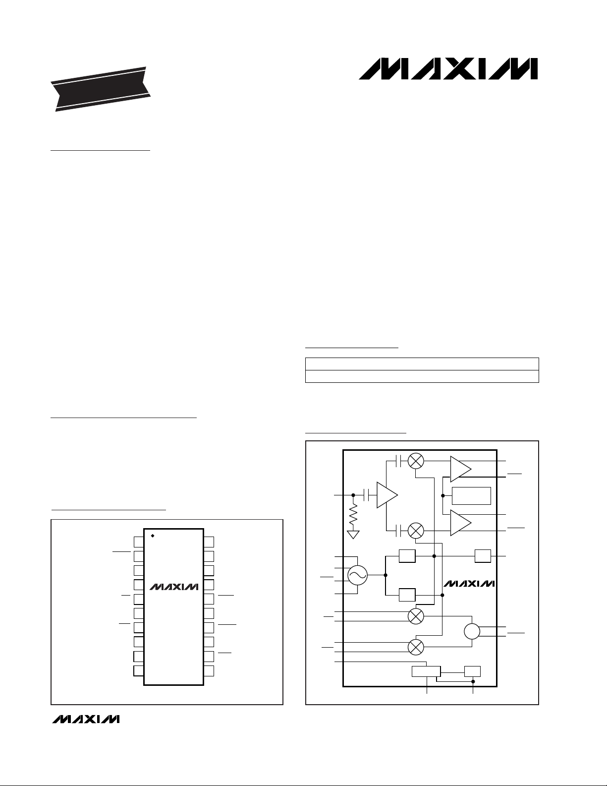
PRESCALER
MODULATOR
DEMODULATOR
QUADRATURE
PHASE
GENERATOR
LOCAL
OSCILLATOR
÷ 2 ÷ 4
BANDGAP BIAS
MASTER BIAS
÷ 2
Σ
0°
90°
MAX2450
Functional Diagram
20
19
18
17
16
15
14
13
1
2
3
4
5
6
7
8
IF_IN
GND
V
CC
I_OUT
I_OUT
Q_OUT
Q_OUT
LO_GND
TANK
TANK
IF_OUT
IF_OUT
GND
I_IN
I_IN
Q_IN
Q_IN
ENABLE
PRE_OUT
LO_V
CC
TOP VIEW
12
11
9
10
QSOP
MAX2450
Pin Configuration
19-0455; Rev 1; 9/98
PART
MAX2450CEP 0°C to +70°C
TEMP. RANGE PIN-PACKAGE
EVALUATION KIT
AVAILABLE
Ordering Information
20 QSOP
Page 2
MAX2450
3V, Ultra-Low-Power Quadrature
Modulator/Demodulator
2 _______________________________________________________________________________________
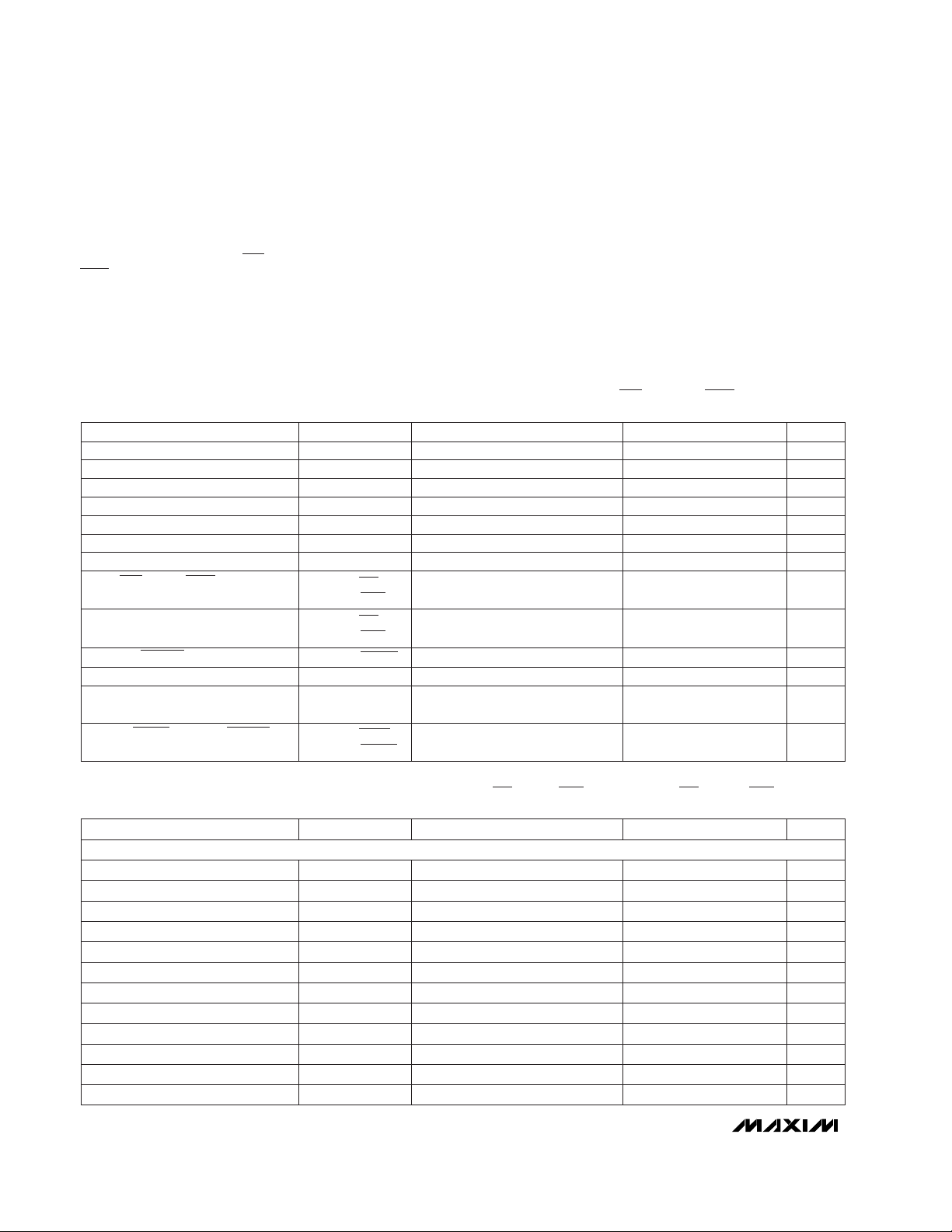
ABSOLUTE MAXIMUM RATINGS
DC ELECTRICAL CHARACTERISTICS
(VCC= LO_VCC= TANK = 2.7V to 3.3V, ENABLE = V
CC
- 0.4, GND = LO_GND = 0V, I_IN = I_IN = Q_IN = Q_IN = IF_IN = TANK =
OPEN, T
A
= 0°C to +70°C, unless otherwise noted.)
Stresses beyond those listed under “Absolute Maximum Ratings” may cause permanent damage to the device. These are stress ratings only, and functional
operation of the device at these or any other conditions beyond those indicated in the operational sections of the specifications is not implied. Exposure to
absolute maximum rating conditions for extended periods may affect device reliability.
VCC, LO_VCCto GND............................................-0.3V to +4.5V
ENABLE, TANK, TANK, I_IN, I_IN
, Q_IN,
Q_IN
to GND..................................................-0.3V to (VCC+ 0.3V)
IF_IN to GND.........................................................-0.3V to +1.5V
Continuous Power Dissipation (T
A
= +70°C)
QSOP (derate 9.1mW/°C above +70°C)......................727mW
Operating Temperature Range...............................0°C to +70°C
Storage Temperature Range.............................-65°C to +165°C
Lead Temperature (soldering, 10sec).............................+300°C
ENABLE = 0.4V
ENABLE = V
CC
CONDITIONS
V1.2
V
I_OUT/I_OUT
,
V
Q_OUT/Q_OUT
I_OUT, I_OUT, Q_OUT, Q_OUT
DC Bias Voltage Level
µA220I
CC(OFF)
Shutdown Supply Current
mA5.9 8.2I
CC(ON)
V2.7 3.3VCC, LO_V
CC
Supply Voltage Range
Supply Current
Ω320 400 480Z
IF_IN
Demodulator IF Input Impedance
VVCC- 1.5V
IF_OUT/IF_OUT
IF_OUT, IF_OUT DC Bias Voltage
kΩ35 44
Z
I_IN/I_IN
,
Z
Q_IN/Q_IN
Modulator Differential Input
Impedance
V1.25 1.5 1.75
V
I_IN/I_IN
,
V
Q_IN/Q_IN
I_IN, I_IN, Q_IN, Q_IN
Self-Bias DC Voltage Level
µs10t
ON/OFF
Enable/Disable Time
µA13I
EN
ENABLE Bias Current
VVCC- 0.4V
ENH
ENABLE High Voltage
V0.4V
ENL
ENABLE Low Voltage
UNITSMIN TYP MAXSYMBOLPARAMETER
AC ELECTRICAL CHARACTERISTICS
(MAX2450 EV kit, VCC= LO_VCC= ENABLE = 3.0V, fLO= 140MHz, f
I_IN/I_IN
= f
Q_IN/Q_IN
= 600kHz, V
I_IN/I_IN
= V
Q_IN/Q_IN
= 1.2V
p-p
,
f
IF_IN
= 70.1MHz, V
IF_IN
= 2.82mV
p-p
, TA= +25°C, unless otherwise noted.)
(Note 2)
(Note 2)
CONDITIONS
dB< ±0.45I and Q Amplitude Balance
dBc-60IM5
I/Q
I and Q IM5 Level
dBc-44IM3
I/Q
I and Q IM3 Level
degrees< ±1.3I and Q Phase Accuracy
dB51Voltage Conversion Gain
UNITSMIN TYP MAXSYMBOLPARAMETER
RL= 10kΩ, CL< 6pF, rising edge
(Notes 1, 3)
10kHz offset
RL= 10kΩ, CL< 6pF
MHz9BW
DEMOD
I and Q Signal 3dB Bandwidth
V/µs60SR
PRE_OUT
PRE_OUT Slew Rate
MHz70 160f
LO
Oscillator Frequency Range
dBc/Hz-80LO Phase Noise
V
p-p
0.35V
PRE_OUT
PRE_OUT Output Voltage
(Note 1) V
p-p
1.35Allowable I and Q Voltage Swing
mV±11 ±50
Demodulator I and Q Baseband
DC Offset
dB18NFNoise Figure
DEMODULATOR
Page 3
MAX2450
3V, Ultra-Low-Power Quadrature
Modulator/Demodulator
_______________________________________________________________________________________
3
7.0
6.8
6.6
6.4
6.2
6.0
5.8
5.6
5.4
5.2
5.0
0
10
20 30 40 50 60 70 80
MAX2450-01
TEMPERATURE (°C)
SUPPLY CURRENT (mA)
SUPPLY CURRENT
vs. TEMPERATURE
V
CC
= 2.7V
V
CC
= 3.3V
V
CC
= 3.0V
0
2
4
6
8
10
12
0
10
20 30 40
50
60 70 80
MAX2450-02
TEMPERATURE (°C)
V
CC
= 2.7V
V
CC
= 3.3V
V
CC
= 3.0V
SHUTDOWN SUPPLY CURRENT
vs. TEMPERATURE
SUPPLY CURRENT (µA)
-30
-34
-38
-42
-46
-50
-54
-26 -22 -18 -14 -10 -6
MAX2450-03
BASEBAND INPUT (dBV
RMS
)
OUTPUT (dBV
RMS
)
MODULATOR IF OUTPUT
vs. BASEBAND INPUT
Vp-p = 2 2 x 10 (V)
dBV
RMS
20
(Note 1)
V
I_IN/I_IN
, = V
Q_IN/Q_IN = 1.2Vp-p,
RL= 200kΩ differential,
CL< 5pF differential
V
I_IN/I_IN
= 1.35Vp-p composite
(Note 4)
V
I_IN/I_IN
= 1.35Vp-p composite
(Note 4)
CONDITIONS
V1.25 1.75Input Common-Mode Voltage Range
V
p-p
1.35
V
I_IN/I_IN
,
V
Q_IN/Q_IN
Allowable Differential Input Voltage
dBc-36
Carrier Suppression at Modulator
Output
dBc38Sideband Rejection
MHz15BW
MOD
I and Q Signal 3dB Bandwidth
mV
p-p
65V
IF_OUT/IF_OUT
IF Differential Output Voltage
dBc-60IM3
IF
IF Output IM3 Level
dBc-60IM5
IF
IF Output IM5 Level
UNITSMIN TYP MAXSYMBOLPARAMETER
AC ELECTRICAL CHARACTERISTICS (continued)
(MAX2450 EV kit, VCC= LO_VCC= ENABLE = 3.0V, fLO= 140MHz, f
I_IN/I_IN
= f
Q_IN/Q_IN
= 600kHz, V
I_IN/I_IN
= V
Q_IN/Q_IN
= 1.2V
p-p
,
f
IF_IN
= 70.1MHz, V
IF_IN
= 2.82mV
p-p
, TA= +25°C, unless otherwise noted.)
MODULATOR
Note 1: Guaranteed by design, not tested.
Note 2: f
IF_IN
= 2 tones at 70.10MHz and 70.11MHz. V
IF_IN
= 1.41mVp-p per tone.
Note 3: The frequency range can be extended in either direction, but has not been characterized. At higher frequencies, the
modulator IF output amplitude may decrease and distortions may increase.
Note 4: Q_IN/Q_IN
ports are terminated. f
I_IN/I_IN
= 2 tones at 550kHz and 600kHz.
__________________________________________Typical Operating Characteristics
(MAX2450 EV kit, VCC= LO_VCC= ENABLE = 3.0V, fLO= 140MHz, f
I_IN/I_IN
= f
Q_IN/Q_IN
= 600kHz, V
I_IN/I_IN
= V
Q_IN/Q_IN
= 1.2V
p-p
,
f
IF_IN
= 70.1MHz, V
IF_IN
= 2.82mV
p-p
, TA= +25°C, unless otherwise noted.)
Page 4

MAX2450
3V, Ultra-Low-Power Quadrature
Modulator/Demodulator
4 _______________________________________________________________________________________
____________________________Typical Operating Characteristics (continued)
(MAX2450 EV kit, VCC= LO_VCC= ENABLE = 3.0V, fLO= 140MHz, f
I_IN/I_IN
= f
Q_IN/Q_IN
= 600kHz, V
I_IN/I_IN
= V
Q_IN/Q_IN
= 1.2V
p-p
,
f
IF_IN
= 70.1MHz, V
IF_IN
= 2.82mV
p-p
, TA= +25°C, unless otherwise noted.)
60
62
64
66
68
70
MODULATOR IF OUTPUT
vs. SUPPLY VOLTAGE
MAX2450-04
VCC (V)
IF OUTPUT (mVp-p)
3.33.23.13.02.92.82.7
TA = +70°C
TA = +25°C
TA = 0°C
60
62
64
66
68
70
MODULATOR IF OUTPUT
vs.TEMPERATURE
MAX2450-05
TEMPERATURE (°C)
IF OUTPUT (mVp-p)
020406080
V
CC
= 3V
-44
-42
-40
-38
-36
-34
-32
-30
MODULATOR SIDEBAND REJECTION
vs. IF FREQUENCY
MAX2450-06
IF FREQUENCY (MHz)
SIDEBAND REJECTION (dBc)
35 40
706560555045
75 80
V
I_IN/I_IN
= 1.2Vp-p
V
Q_IN/Q_IN
= 1.2Vp-p
-44
-42
-40
-38
-36
MODULATOR SIDEBAND REJECTION
vs. TEMPERATURE
MAX2450-07
TEMPERATURE (°C)
SIDEBAND REJECTION (dBc)
020406080
V
I_IN/I_IN
= 1.2Vp-p
V
Q_IN/Q_IN
= 1.2Vp-p
-44
-42
-40
-38
-36
-34
-32
-30
CARRIER SUPPRESSION
vs. IF FREQUENCY
MAX2450-08
IF FREQUENCY (MHz)
CARRIER SUPPRESSION (dBc)
35 40
706560555045
75 80
V
I_IN/I_IN
= 1.2Vp-p
V
Q_IN/Q_IN
= 1.2Vp-p
100mV/
div
PRE_OUT WAVEFORM
MAX2450-09
20ns/div
RL = 10kΩ
C
L
< 6pF
-60
69.0 70.6
71.0
MODULATOR OUTPUT SPECTRUM
-50
0
MAX2450-10
(MHz)
(dBc)
69.4 70.0
-20
-10
-30
-40
V
I_IN/I_IN
= 1.2Vp-p
V
Q_IN/Q_IN
= 1.2Vp-p
Page 5

MAX2450
3V, Ultra-Low-Power Quadrature
Modulator/Demodulator
_______________________________________________________________________________________
5
48.0
48.5
49.0
49.5
50.0
50.5
51.0
51.5
DEMODULATOR VOLTAGE CONVERSION
GAIN vs. TEMPERATURE AND SUPPLY
MAX2450-11
GAIN (dBV)
2.6 2.7 2.8 2.9 3.0 3.1 3.2 3.3 3.4
VCC (V)
TA = +50°C
TA = +25°C
TA = 0°C
TA = +70°C
50.6
50.8
51.0
51.2
51.4
DEMODULATOR VOLTAGE CONVERSION
GAIN vs. IF FREQUENCY
MAX2450-12
IF FREQUENCY (MHz)
GAIN (dBV)
35 40
706560555045
75 80
51
50
49
48
47
46
45
44
43
42
DEMODULATOR VOLTAGE CONVERSION
GAIN vs. BASEBAND FREQUENCY
MAX2450-13
BASEBAND FREQUENCY (Hz)
GAIN (dBV)
100M10M1M100k10k
____________________________Typical Operating Characteristics (continued)
(MAX2450 EV kit, VCC= LO_VCC= ENABLE = 3.0V, fLO= 140MHz, f
I_IN/I_IN
= f
Q_IN/Q_IN
= 600kHz, V
I_IN/I_IN
= V
Q_IN/Q_IN
= 1.2V
p-p
,
f
IF_IN
= 70.1MHz, V
IF_IN
= 2.82mV
p-p
, TA= +25°C, unless otherwise noted.)
0.4
0.8
0.6
1.0
1.2
1.4
1.6
DEMODULATOR I/Q PHASE
AND AMPLITUDE MISMATCH
vs. TEMPERATURE
MAX2450-15
TEMPERATURE (°C)
MATCHING (DEGREES OR dBV)
010
706050403020
PHASE MATCH
AMPLITUDE MATCH
-65
-60
-55
-50
-45
-40
DEMODULATOR INTERMOD POWER
vs. TEMPERATURE
MAX2450-16
TEMPERATURE (°C)
INTERMODULATION (dBc)
010
706050403020
IM3
IM5
f
OSC
= 140MHz
f
IF1
= 70.1MHz
f
IF2
= 70.11MHz
V
IF_IN
= 2.82mVp-p
Page 6

MAX2450
3V, Ultra-Low-Power Quadrature
Modulator/Demodulator
6 _______________________________________________________________________________________
______________________________________________________________Pin Description
Local-Oscillator, Divide-by-8, Prescaled OutputPRE_OUT9
Local-Oscillator Supply. Bypass separately from VCC.LO_V
CC
10
Local-Oscillator Resonant Tank Input (Figure 4)TANK11
Local-Oscillator Resonant Tank Inverting Input (Figure 4)
TANK
12
Local-Oscillator GroundLO_GND13
Baseband Inphase Inverting InputI_IN5
Baseband Quadrature InputQ_IN6
Baseband Quadrature Inverting InputQ_IN7
Enable Control, active highENABLE8
Baseband Inphase InputI_IN4
GroundGND3, 19
PIN
Modulator IF Inverting OutputIF_OUT2
Modulator IF OutputIF_OUT1
FUNCTIONNAME
Demodulator Inphase Inverting OutputI_OUT16
Demodulator Inphase OutputI_OUT17
Modulator and Demodulator SupplyV
CC
18
Demodulator IF InputIF_IN20
Demodulator Quadrature Inverting OutputQ_OUT14
Demodulator Quadrature OutputQ_OUT15
Figure 1. Typical Application Block Diagram
2
A/D
CONVERSION
÷ 8
UP/DOWNCONVERTER
Σ
0°
90°
MAX2450
2
A/D
CONVERSION
2
D/A
CONVERSION
2
D/A
CONVERSION
R
T
DSP
Page 7

_______________Detailed Description
The following sections describe each of the functional
blocks shown in the
Functional Diagram
. They also refer
to the Typical Application Block Diagram (Figure 1).
Demodulator
The demodulator contains a single-ended-to-differential
converter, two Gilbert-cell multipliers, and two fixed gain
stages. The IF signal should be AC coupled into IF_IN.
Internally, IF_IN is terminated with a 400Ω resistor to
GND and provides a gain of 14dB. This amplified IF signal is fed into the I and Q mixers for demodulation. The
multipliers mix the IF signal with the quadrature LO signals, resulting in baseband I and Q signals. The conversion gain of the multipliers is 15dB. These signals are
further amplified by 21dB by the baseband amplifiers.
The baseband I and Q amplifier chains are DC coupled.
Local Oscillator
The local-oscillator section is formed by an emitter-coupled differential pair. Figure 2 shows the equivalent
local-oscillator circuit schematic. An external LC resonant tank determines the oscillation frequency, and the
Q of this resonant tank affects the oscillator phase
noise. The oscillation frequency is twice the IF frequency, so that the quadrature phase generator can use two
latches to generate precise quadrature signals.
The oscillator may be overdriven by an external source.
The source should be AC coupled into TANK/TANK,
and should provide 200mVp-p levels. A choke (typically
2.2µH) is required between TANK and TANK. Differential input impedance at TANK/TANK is 10kΩ. For single-ended drive, connect an AC bypass capacitor
(1000pF) from TANK to GND, and AC couple TANK to
the source.
Quadrature Phase Generator
The quadrature phase generator uses two latches to
divide the local-oscillator frequency by two, and generates two precise quadrature signals. Internal limiting
amplifiers shape the signals to approximate square
waves to drive the Gilbert-cell mixers. The inphase signal (at half the local-oscillator frequency) is further
divided by four for the prescaler output.
Prescaler
The prescaler output, PRE_OUT, is buffered and swings
typically 0.35V
p-p
with a 10kΩ and 6pF load. It can be
AC-coupled to the input of a frequency synthesizer.
Modulator
The modulator accepts I and Q differential baseband
signals up to 1.35V
p-p
with frequencies up to 15MHz,
and upconverts them to the IF frequency. Since these
inputs are biased internally at around 1.5V, I and Q signals should be capacitively coupled into these highimpedance ports (the differential input impedance is
approximately 44kΩ). The self-bias design yields very
low on-chip offset, resulting in excellent carrier sup-
MAX2450
3V, Ultra-Low-Power Quadrature
Modulator/Demodulator
_______________________________________________________________________________________ 7
Figure 2. Local-Oscillator Equivalent Circuit
R
L
5k
R
L
5k
Q1
Q3 Q4
TO
QUADRATURE
GENERATOR AND
PRESCALER
Q2
TANKTANK
LO_V
CC
Figure 3. Modulator Output Level vs. Load Resistance
35
40
45
50
55
60
65
70
75
MAX2450-fig03
LOAD RESISTANCE (Ω)
OUTPUT LEVEL (mVp-p)
200
1k 10k 100k
Page 8

MAX2450
3V, Ultra-Low-Power Quadrature
Modulator/Demodulator
Maxim cannot assume responsibility for use of any circuitry other than circuitry entirely embodied in a Maxim product. No circuit patent licenses are
implied. Maxim reserves the right to change the circuitry and specifications without notice at any time.
8
_____________________Maxim Integrated Products, 120 San Gabriel Drive, Sunnyvale, CA 94086 408-737-7600
© 1998 Maxim Integrated Products Printed USA is a registered trademark of Maxim Integrated Products.
pression. Alternatively, a differential DAC may be connected without AC coupling, as long as a commonmode voltage range of 1.25V to 1.75V is maintained.
For single-ended drive, connect I_IN and Q_IN via ACcoupling capacitors (0.1µF) to GND.
The IF output is designed to drive a high impedance
(> 20kΩ), such as an IF buffer or an upconverter
mixer. IF_OUT/IF_OUT must be AC coupled to the
load. Impedances as low as 200Ω can be driven with a
decrease in output amplitude (Figure 3). To drive a single-ended load, AC couple and terminate IF_OUT with
a resistive load equal to the load at IF_OUT.
Master Bias
During normal operation, ENABLE should remain above
VCC- 0.4V. Pulling the ENABLE input low shuts off the
master bias and reduces the circuit current to less than
2µA. The master bias section includes a bandgap reference generator and a PTAT (Proportional To Absolute
Temperature) current generator.
__________Applications Information
Figure 4 shows the implementation of a resonant tank
circuit. The inductor, two capacitors, and a dual varactor form the oscillator’s resonant circuit. In Figure 4, the
oscillator frequency ranges from 130MHz to 160MHz.
To ensure reliable start-up, the inductor is directly connected across the local oscillator’s tank ports. The two
33pF capacitors affect the Q of the resonant circuit.
Other values may be chosen to meet individual application requirements. Use the following formula to determine the oscillation frequency:
where C
STRAY
= parasitic capacitance and L
STRAY
=
parasitic inductance.
To alter the oscillation frequency range, change the
inductance, the capacitance, or both. For best phasenoise performance keep the Q of the resonant tank as
high as possible:
where R
EQ
≈ 10kΩ (Figure 2).
The oscillation frequency can be changed by altering
the control voltage, V
CTRL
.
QR
EQ
C
L
EQ
EQ
=
f
1
2LC
where
C
1
1C11
C22C
C
and
L L L
o
EQ EQ
EQ
VAR
STRAY
EQ STRAY
=
=
++
+
=+
π
Figure 4. Typical Resonant Tank Circuit
L = 100nH
C2 = 33pF
C1 = 33pF 47k
10k
47k
1
/2 KV1410
1
/2 KV1410
TANK
TANK
V
CTRL
0.1µF
 Loading...