

Page 1
For free samples & the latest literature: http://www.maxim-ic.com, or phone 1-800-998-8800.
For small orders, phone 408-737-7600 ext. 3468.
________________General Description
The MAX2411A performs the RF front-end transmit/
receive function in time-division-duplex (TDD) communication systems. It operates over a wide frequency range
and is optimized for RF frequencies around 1.9GHz.
Applications include most popular cordless and PCS
standards. The MAX2411A includes a low-noise amplifier
(LNA), a downconverter mixer, a local-oscillator buffer, an
upconverter mixer, and a variable-gain power-amplifier
(PA) driver in a low-cost, plastic surface-mount package.
The MAX2411A’s unique bidirectional, differential IF port
reduces cost and component count by allowing the transmit and receive paths to share the same IF filter.
The LNA has a 2.4dB typical noise figure and a -10dBm
input third-order intercept point (IP3). The downconverter mixer has a low 9.2dB noise figure and 4dBm input
IP3. Image and local-oscillator filtering are implemented
off-chip for maximum flexibility. The PA driver amplifier
has 15dB of gain, which can be reduced over a 35dB
range. Power consumption is only 60mW in receive
mode and 90mW in transmit mode and drops to less
than 3µW in shutdown mode.
For applications requiring separate, single-ended IF
input and output ports, refer to the MAX2410 data
sheet. For applications requiring only a receive function, Maxim offers a low-cost downconverter with LNA
(see the MAX2406 data sheet).
________________________Applications
PWT1900 DECT
DCS1800/PCS1900 ISM-Band Transceivers
PHS/PACS Iridium Handsets
____________________________Features
♦ Low-Cost Silicon Bipolar Design
♦ Integrated Upconvert/Downconvert Function
♦ Operates from a Single +2.7V to +5.5V Supply
♦ 3.2dB Combined Receiver Noise Figure:
2.4dB (LNA)
9.2dB (mixer)
♦ Flexible Power-Amplifier Driver:
18dBm Output Third-Order Intercept (OIP3)
35dB Gain-Control Range
♦ LO Buffer for Low LO Drive Level
♦ Low Power Consumption:
60mW Receive
90mW Full-Power Transmit
♦ 0.3µW Shutdown Mode
♦ Flexible Power-Down Modes Compatible with
MAX2510/MAX2511 IF Transceivers
MAX2411A
Low-Cost RF Up/Downconverter
with LNA and PA Driver
________________________________________________________________
Maxim Integrated Products
1
28
27
26
25
24
23
22
21
20
19
18
17
16
15
1
2
3
4
5
6
7
8
9
10
11
12
13
14
GND
LNAOUT
GND
GND
RXMXIN
GND
GND
IF
IF
GND
TXMXOUT
GND
GND
PADRIN
GND
PADROUT
GND
GC
V
CC
TXEN
LO
LO
RXEN
V
CC
GND
GND
LNAIN
GND
QSOP
TOP VIEW
MAX2411A
19-1324; Rev 1; 2/98
PART
MAX2411AEEI -40°C to +85°C
TEMP. RANGE PIN-PACKAGE
28 QSOP
EVALUATION KIT
AVAILABLE
_______________Ordering Information
Typical Operating Circuit appears on last page.
MAX2411AE/D -40°C to +85°C Dice*
*
Dice are specified at TA= 25°C, DC parameters only.
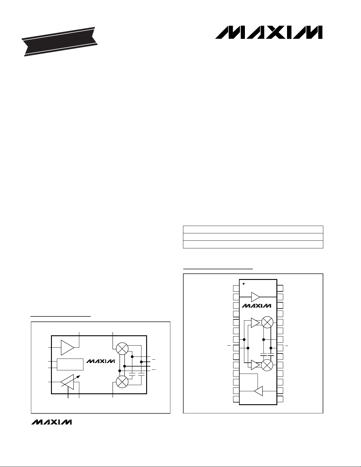
Functional Diagram
Pin Configuration
LNAOUT RXMXIN
MAX2411A
PA DRIVER
MANAGEMENT
LNA
POWER
PADRINGC
LNAIN
RXEN
TXEN
PADROUT
TXMXOUT
RX MIXER
TX MIXER
IF
IF
LO
LO
Page 2
MAX2411A
Low-Cost RF Up/Downconverter
with LNA and PA Driver
2 _______________________________________________________________________________________
ABSOLUTE MAXIMUM RATINGS
DC ELECTRICAL CHARACTERISTICS
(VCC= +2.7V to +5.5V, VGC= +3.0V, RXEN = TXEN = 0.6V, PADROUT pulled up to VCCwith 50Ω resistor; IF, IF pulled up to V
CC
with 50Ω resistor, TXMXOUT pulled up to VCCwith 125Ω resistor, LNAOUT pulled up to VCCwith 100Ω resistor, all RF inputs open,
T
A
= -40°C to +85°C. Typical values are at +25°C and VCC= +3.0V, unless otherwise noted.)
AC ELECTRICAL CHARACTERISTICS
(MAX2411A EV kit, VCC= +3.0V, VGC= +2.15V, RXEN = TXEN = low, all measurements performed in 50Ω environment,
f
LO
= 1.5GHz, PLO= -10dBm, f
LNAIN
= f
PADRIN
= f
RXMXIN
= 1.9GHz, P
LNAIN
= -32dBm, P
PADRIN
= P
RXMXIN
= -22dBm,
f
IF, IF
= 400MHz, PIF= -32dBm (Note 1), TA= +25°C, unless otherwise noted.)
Stresses beyond those listed under “Absolute Maximum Ratings” may cause permanent damage to the device. These are stress ratings only, and functional
operation of the device at these or any other conditions beyond those indicated in the operational sections of the specifications is not implied. Exposure to
absolute maximum rating conditions for extended periods may affect device reliability.
VCCto GND ................................................................-0.3V to 6V
LNAIN Input Power...........................................................15dBm
LO, LO Input Power..........................................................10dBm
PADRIN Input Power.........................................................10dBm
RXMXIN Input Power ........................................................10dBm
IF, IF Input Power (transmit mode) ...................................10dBm
Voltage at RXEN, TXEN, GC.......................-0.3V to (V
CC
+ 0.3V)
Continuous Power Dissipation (T
A
= +70°C)
QSOP (derate 11mW/°C above +70°C)........................909mW
Junction Temperature......................................................+150°C
Operating Temperature Range ...........................-40°C to +85°C
Storage Temperature.........................................-65°C to +165°C
Lead Temperature (soldering, 10sec).............................+300°C
RXEN, TXEN pins
RXEN, TXEN pins
VCC= 3.0V
RXEN = 2.0V, TXEN = 2.0V
RXEN = 2.0V
TXEN = 2.0V
RXEN = 2.0V
TXEN = 2.0V
CONDITIONS
µA0.1 10Supply Current, Shutdown Mode
V0.6Digital Input Voltage Low
V2.0
V2.7 5.5Supply-Voltage Range
Digital Input Voltage High
µA160 520Supply Current, Standby Mode
µA0.1 1RXEN Input Bias Current (Note 1)
µA0.1 1TXEN Input Bias Current (Note 1)
mA20 29.6Supply Current, Receive Mode
mA30 44.7Supply Current, Transmit Mode
UNITSMIN TYP MAXPARAMETER
TA= T
MIN
to T
MAX
TA= +25°C
(Note 3)
RXEN = high or low
CONDITIONS
dB
12.6 19.1
Gain (Note 2)
14.2 16.2 17.4
dB2.4Noise Figure
dBm-10Input IP3
dBm-5Output 1dB Compression
dBm-49LO to LNAIN Leakage
UNITSMIN TYP MAXPARAMETER
TA= -40°C to +85°C
TA= +25°C
Single sideband
(Note 4)
(Notes 2, 5)
dB
7.5 10.9
Conversion Gain (Note 2)
8.5 9.4 10.0
dB9.2Noise Figure
dBm4.0Input IP3
dBm-7.7Input 1dB Compression
MHz450IF Frequency
(Note 6) dBm-17Minimum LO Drive Level
LOW-NOISE AMPLIFIER (RXEN = high)
RECEIVE MIXER (RXEN = high)
GC = 3V, TXEN = 2V µA35 51.1GC Input Bias Current
Page 3

MAX2411A
Low-Cost RF Up/Downconverter
with LNA and PA Driver
_______________________________________________________________________________________ 3
AC ELECTRICAL CHARACTERISTICS (continued)
(MAX2411A EV kit, VCC= +3.0V, VGC= +2.15V, RXEN = TXEN = low, all measurements performed in 50Ω environment,
f
LO
= 1.5GHz, PLO= -10dBm, f
LNAIN
= f
PADRIN
= f
RXMXIN
= 1.9GHz, P
LNAIN
= -32dBm, P
PADRIN
= P
RXMXIN
= -22dBm,
f
IF, IF
= 400MHz, PIF= -32dBm (Note 1), all impedance measurements made directly to pin (no matching network), TA= +25°C,
unless otherwise noted.)
Note 1: Power delivered to IF SMA connector of MAX2411A EV kit. Power delivered to MAX2411A IC is approximately 1.0dB less
due to balun losses.
Note 2: Guaranteed by design and characterization.
Note 3: Two tones at 1.9GHz and 1.901GHz at -32dBm per tone.
Note 4: Two tones at 1.9GHz and 1.901GHz at -22dBm per tone.
Note 5: Mixer operation guaranteed to this frequency. For optimum gain, adjust output match. See the
Typical Operating
Characteristics
for graphs of IF port impedance versus IF frequency.
Note 6: At this LO drive level, the mixer conversion gain is typically 1dB lower than with -10dBm LO drive.
Note 7: Two tones at 400MHz and 401MHz at -32dBm per tone.
Note 8: Transmit mixer output at -17dBm.
Note 9: Calculated from measurements taken at V
GC
= 1.0V and VGC= 1.5V.
Note 10: Time from RXEN = low to RXEN = high transition until the combined receive gain is within 1dB of its final value. Measured
with 47pF blocking capacitors on LNAIN and LNAOUT.
Note 11: Time from TXEN = low to TXEN = high transition until the combined transmit gain is within 1dB of its final value. Measured
with 47pF blocking capacitors on PADRIN and PADROUT.
CONDITIONS UNITSMIN TYP MAXPARAMETER
TA= +25°C 6.8 8.5 9.3
(Notes 1, 7) dBm0.5Output IP3
TA= T
MIN
to T
MAX
dB
5.7 10.4
Conversion Gain (Note 1)
dBm-58LO Leakage
(Notes 2, 5) MHz450IF Frequency
Single sideband dB8.3Noise Figure
dBm-11.1Output 1dB Compression Point
F
OUT
= 2LO-3IF = 1.8GHz -70
F
OUT
= 2LO-2IF = 2.2GHz -45.5
TA= T
MIN
to T
MAX
dB
12.3 17
F
OUT
= 3LO-6IF = 2.1GHz
Gain (Note 2)
TA= +25°C 13 15 16.4
dBc
-90
Intermod Spurious Response
(Note 8)
(Note 4) dBm18Output IP3
dB35Gain-Control Range
dBm6.3Output 1dB Compression Point
(Note 9) dB/V12Gain-Control Sensitivity
Receive mode (TXEN = low) 1.10
Transmit mode (RXEN = low) 1.02
Input Relative VSWR
TXEN = low to high µs0.3 2.5Transmitter Turn-On Time (Notes 2, 11)
RXEN = low to high µs0.5 2.5Receiver Turn-On Time (Notes 2, 10)
TRANSMIT MIXER (TXEN = high)
PA DRIVER (TXEN = high)
POWER MANAGEMENT (RXEN = TXEN = low)
LOCAL-OSCILLATOR INPUTS (RXEN = TXEN = high)
Page 4
MAX2411A
Low-Cost RF Up/Downconverter
with LNA and PA Driver
4 _______________________________________________________________________________________
__________________________________________Typical Operating Characteristics
(MAX2411A EV kit, VCC= +3.0V, VGC= +2.15V, RXEN = TXEN = low, all measurements performed in 50Ω environment,
fLO= 1.5GHz, PLO= -10dBm, f
LNAIN
= f
PADRIN
= f
RXMXIN
= 1.9GHz, P
LNAIN
= -32dBm, P
PADRIN
= P
RXMXIN
= -22dBm,
f
IF, IF
= 400MHz, PIF= -32dBm (Note 1), all impedance measurements made directly to pin (no matching network), TA= +25°C,
unless otherwise noted.)
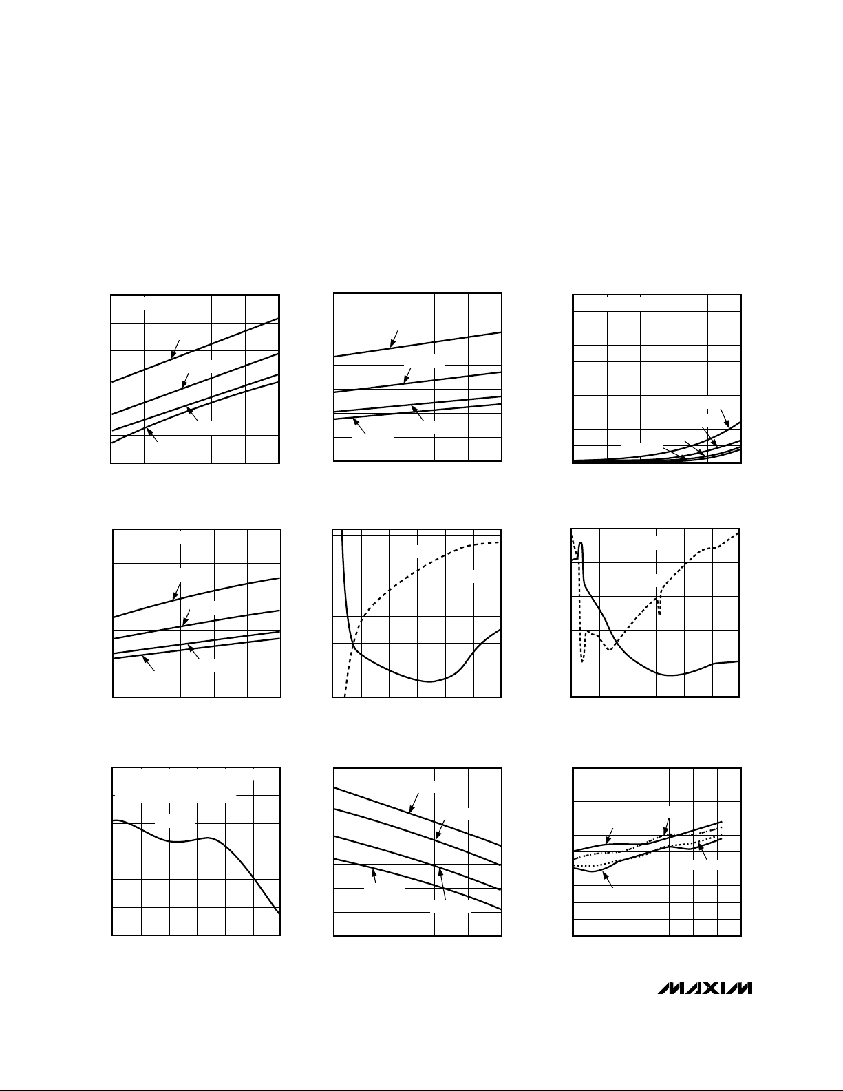
26
30
28
34
32
36
38
-40 10-15 35 60 85
TRANSMIT-MODE SUPPLY CURRENT
vs. TEMPERATURE
MAX2411A-01
TEMPERATURE (°C)
TRANSMITTER SUPPLY CURRENT (mA)
VCC = 5.5V
TXEN = V
CC
VCC = 4.0V
VCC = 2.7V
VCC = 3.0V
17
19
18
21
20
23
22
24
-40 10-15 35 60 85
RECEIVE-MODE SUPPLY CURRENT
vs. TEMPERATURE
MAX2411A-02
TEMPERATURE (°C)
RECEIVE SUPPLY CURRENT (mA)
VCC = 5.5V
RXEN = V
CC
VCC = 4.0V
VCC = 2.7V
VCC = 3.0V
0
0.03
0.02
0.01
0.04
0.05
0.06
0.07
0.08
0.09
0.10
-40 10-15 35 60 85
SHUTDOWN SUPPLY CURRENT
vs. TEMPERATURE
MAX2411A-03
TEMPERATURE (°C)
SHUTDOWN SUPPLY CURRENT (µA)
VCC = 5.5V
RXEN = TXEN = GND
VCC = 4.0V
VCC = 2.7V
VCC = 3.0V
0
100
300
200
400
500
-40 10-15 35 60 85
STANDBY SUPPLY CURRENT
vs. TEMPERATURE
MAX2411A-04
TEMPERATURE (°C)
STANDBY SUPPLY CURRENT (µA)
VCC = 5.5V
RXEN = TXEN = 2.0V
VCC = 4.0V
VCC = 2.7V
VCC = 3.0V
0
10
5
20
15
25
30
0 1.0 1.50.5 2.0 2.5 3.0
LNA GAIN vs. FREQUENCY
MAX2411A-07
FREQUENCY (GHz)
LNA GAIN (dB)
1pF SHUNT CAPACITOR AT LNA INPUT
USING EV KIT MATCHING CIRCUIT
(OPTIMIZED FOR 1.9GHz)
RXEN = V
CC
0
40
20
80
60
100
120
0 1.0 1.50.5 2.0 2.5 3.0
LNA INPUT IMPEDANCE
vs. FREQUENCY
MAX2411A-05
FREQUENCY (GHz)
REAL IMPEDANCE (Ω)
-200
-120
-160
-40
-80
0
40
IMAGINARY IMPEDANCE (Ω)
IMAGINARY
REAL
RXEN = V
CC
0
50
150
100
200
250
0 1.00.5 1.5 2.0 2.5 3.0
LNA OUTPUT IMPEDANCE
vs. FREQUENCY
MAX2411A-06
FREQUENCY (GHz)
REAL IMPEDANCE (Ω)
-125
-100
-50
-75
-25
0
IMAGINARY IMPEDANCE (Ω)
IMAGINARY
REAL
RXEN = V
CC
13
15
14
17
16
19
18
20
-40 10-15 35 60 85
LNA GAIN vs. TEMPERATURE
MAX2411A-08
TEMPERATURE (°C)
LNA GAIN (dB)
VCC = 5.5V
VCC = 4.0V
VCC = 2.7V
VCC = 3.0V
RXEN = V
CC
-15
-12
-13
-14
-10
-11
-6
-7
-8
-9
-5
-40 -20 0 20 40 60 10080
LNA INPUT IP3 vs. TEMPERATURE
MAX2411A-09
TEMPERATURE (°C)
INPUT IP3 (dBm)
VCC = 5.5V
VCC = 4.0V
VCC = 2.7V
VCC = 3.0V
RXEN = V
CC
Page 5
MAX2411A
Low-Cost RF Up/Downconverter
with LNA and PA Driver
_______________________________________________________________________________________
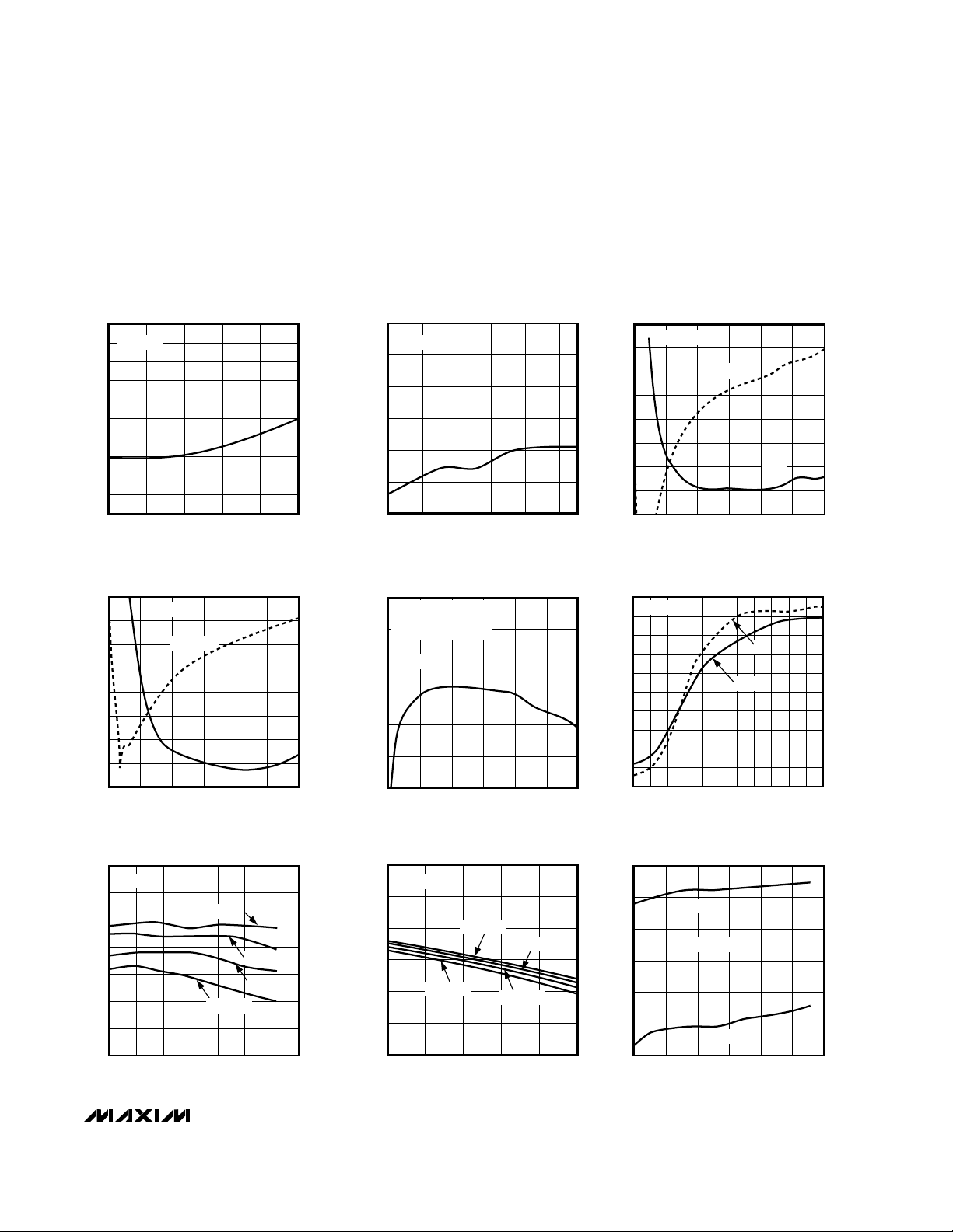
5
0.0
1.0
0.5
2.0
1.5
3.0
2.5
3.5
4.5
4.0
5.0
100 480 860 1240 1620 2000
LNA NOISE FIGURE vs. FREQUENCY
MAX2411A-10
FREQUENCY (MHz)
NOISE FIGURE (dB)
RXEN = V
CC
-6
-4
-5
-2
-3
-1
0
2.7 3.7 4.23.2 4.7 5.2
LNA OUTPUT 1dB COMPRESSION POINT
vs. SUPPLY VOLTAGE
MAX2411A-11
SUPPLY VOLTAGE (V)
OUTPUT 1dB COMPRESSION POINT (dBm)
RXEN = V
CC
0
20
40
60
80
100
120
140
-250
-210
-170
-130
-90
-50
-10
30
160 70
0 1.00.5 1.5 2.0 2.5 3.0
PA DRIVER INPUT IMPEDANCE
vs. FREQUENCY
MAX2411A-12
FREQUENCY (GHz)
REAL IMPEDANCE (Ω)
IMAGINARY IMPEDANCE (Ω)
IMAGINARY
REAL
TXEN = V
CC
0
25
50
75
100
125
150
175
200
-350
-300
-250
-200
-150
-100
-50
0
50
0 1.00.5 1.5 2.0 2.5 3.0
PA DRIVER OUTPUT IMPEDANCE
vs. FREQUENCY
MAX2411A-13
FREQUENCY (GHz)
REAL IMPEDANCE (Ω)
IMAGINARY IMPEDANCE (Ω)
IMAGINARY
REAL
TXEN = V
CC
14
16
15
18
17
20
19
21
-40 0 20-20 40 60 10080
PA DRIVER OUTPUT IP3
vs. TEMPERATURE
MAX2411A-16
TEMPERATURE (°C)
OUTPUT IP3 (dBm)
VCC = 5.5V
VCC = 4.0V
VCC = 2.7V
VCC = 3.0V
TXEN = V
CC
0
10
5
20
15
25
30
0 1.0 1.50.5 2.0 2.5 3.0
PA DRIVER GAIN vs. FREQUENCY
MAX2411A-14
FREQUENCY (GHz)
GAIN (dB)
USING EV KIT
MATCHING NETWORK
(OPTIMIZED FOR 1.9GHz)
TXEN = V
CC
-30
-20
-25
-5
-10
-15
0
5
15
10
20
0 0.4 0.60.2 0.8 1.0 1.2 1.4 1.6 1.8 2.0 2.2
PA DRIVER GAIN AND OUTPUT IP3
vs. GC VOLTAGE
MAX2411A-15
GC VOLTAGE (V)
GAIN (dB) OR OUTPUT IP3 (dBm)
IP3
GAIN
TXEN = V
CC
12
14
13
16
15
17
18
-40 10-15 35 60 85
PA DRIVER GAIN vs. TEMPERATURE
MAX2411A-17
TEMPERATURE (°C)
PA DRIVER GAIN (dB)
VCC = 5.5V
VCC = 4.0V
VCC = 2.7V
VCC = 3.0V
TXEN = V
CC
-4
0
-2
4
2
6
8
2.7 3.7 4.23.2 4.7 5.75.2
PA DRIVER OUTPUT 1dB COMPRESSION
vs. SUPPLY VOLTAGE
MAX2411A-18
SUPPLY VOLTAGE (V)
OUTPUT 1dB COMPRESSION POINT (dBm)
VGC = 2.15V
VGC = 1.0V
TXEN = V
CC
_____________________________Typical Operating Characteristics (continued)
(MAX2411A EV kit, VCC= +3.0V, VGC= +2.15V, RXEN = TXEN = low, all measurements performed in 50Ω environment, fLO= 1.5GHz,
PLO= -10dBm, f
LNAIN
= f
PADRIN
= f
RXMXIN
= 1.9GHz, P
LNAIN
= -32dBm, P
PADRIN
= P
RXMXIN
= -22dBm, f
IF, IF
= 400MHz,
PIF= -32dBm (Note 1), all impedance measurements made directly to pin (no matching network), TA= +25°C, unless otherwise noted.)
Page 6

MAX2411A
Low-Cost RF Up/Downconverter
with LNA and PA Driver
6 _______________________________________________________________________________________
_____________________________Typical Operating Characteristics (continued)
(MAX2411A EV kit, VCC= +3.0V, VGC= +2.15V, RXEN = TXEN = low, all measurements performed in 50Ω environment, fLO= 1.5GHz,
PLO= -10dBm, f
LNAIN
= f
PADRIN
= f
RXMXIN
= 1.9GHz, P
LNAIN
= -32dBm, P
PADRIN
= P
RXMXIN
= -22dBm, f
IF, IF
= 400MHz,
PIF= -32dBm (Note 1), all impedance measurements made directly to pin (no matching network), TA= +25°C, unless otherwise noted.)
0
2
1
4
3
6
5
7
9
8
10
0 0.4 0.6 0.80.2 1.0 1.2 1.4 1.81.6 2.0
PA DRIVER
NOISE FIGURE vs. FREQUENCY
MAX2411A-19
FREQUENCY (GHz)
NOISE FIGURE (dB)
TXEN = V
CC
0
10
5
20
15
25
30
0 1.0 1.50.5 2.0 2.5 3.0
PA DRIVER NOISE FIGURE
vs. GAIN-CONTROL VOLTAGE
MAX2411A-20
GAIN-CONTROL VOLTAGE (V)
NOISE FIGURE (dB)
TXEN = V
CC
0
10
30
20
40
100
80
90
70
60
50
-200
-180
-140
-160
-20
-40
-60
-80
-100
-120
0
0.0 1.00.5 1.5 2.0 2.5 3.0
RECEIVE MIXER INPUT IMPEDANCE
vs. FREQUENCY
FREQUENCY (GHz)
REAL IMPEDANCE (Ω)
MAX2410A-21
IMAGINARY IMPEDANCE (Ω)
IMAGINARY
REAL
RXEN = V
CC
2
5
4
3
V
CC
= 2.7V
V
CC
= 5.5V
9
8
7
6
10
11
12
-40 20 40-20 0 60 80
RECEIVE MIXER CONVERSION
GAIN vs. TEMPERATURE
MAX2411Atoc22
TEMPERATURE (°C)
CONVERSION GAIN (dB)
RXEN = V
CC
4
6
5
8
7
10
9
11
13
12
NOISE FIGURE
GAIN
14
-18 -14 -12 -10-16 -8 -6 -4 -2 0
RECEIVE MIXER GAIN AND NOISE FIGURE
vs. LO POWER
MAX2411Atoc25
LO POWER (dBm)
GAIN AND NOISE FIGURE (dB)
RXEN = V
CC
0
2
1
V
CC
= 2.7V
V
CC
= 5.5V
V
CC
= 4.0V
4
3
5
6
-40 20 40-20 0 60 80
RECEIVE MIXER INPUT IP3
vs. TEMPERATURE
MAX2411Atoc23
TEMPERATURE (°C)
INPUT IP3 (dBm)
V
CC
= 3.0V
RXEN = V
CC
-2
4
2
0
6
8
10
12
14
16
NARROW BAND MATCH
AT RXMXIN, EV KIT
MATCH AT IF, IF
EV KIT
MATCHING NETWORK
AT RXMXIN AND IFOUT
IF = 400MHz
18
0.5 1.51.0 2.0 2.5 3.0
RECEIVE MIXER CONVERSION GAIN
vs. RF FREQUENCY
MAX2411A toc24
RF FREQUENCY (GHz)
CONVERSION GAIN (dB)
RXEN = V
CC
0
200
600
400
800
1000
-1200
-1500
-600
-900
-300
REAL
IMAGINARY
SINGLE-ENDED
0
0 400200 600 800 1000
MAX2411Atoc26
FREQUENCY (MHz)
REAL IMPEDANCE (Ω)
IMAGINARY IMPEDANCE (Ω)
IF OR IF OUTPUT IMPEDANCE
vs. FREQUENCY
RXEN = V
CC
-100
-50
0
50
100
150
200
250
300
-200
-175
-150
-125
-100
-75
-50
-25
0
0 1.00.5 1.5 2.0 2.5 3.0
TRANSMIT MIXER OUTPUT IMPEDANCE
vs. FREQUENCY
MAX2411A-27
FREQUENCY (GHz)
REAL IMPEDANCE (Ω)
IMAGINARY IMPEDANCE (Ω)
IMAGINARY
REAL
TXEN = V
CC
Page 7

MAX2411A
Low-Cost RF Up/Downconverter
with LNA and PA Driver
_______________________________________________________________________________________
7
0
4
2
V
CC
= 2.7V
V
CC
= 5.5V
V
CC
= 4.8V
8
6
10
12
-40 20 40-20 0 60 80
TRANSMIT MIXER CONVERSION GAIN
vs. TEMPERATURE
MAX2411Atoc28
TEMPERATURE (°C)
CONVERSION GAIN (dB)
TXEN = V
CC
0
3
2
1
4
5
6
7
8
9
10
0.5 1.51.0 2.0 2.5 3.0
TRANSMIT MIXER CONVERSION GAIN
vs. RF FREQUENCY
MAX2411Atoc29
RF FREQUENCY (GHz)
CONVERSION GAIN (dB)
NARROW BAND AT TXMXOUT,
EV KIT MATCH AT IF, IF
EV KIT MATCH NETWORK
AT TXMXOUT AND IF, IF
IF = 400MHz
TXEN = V
CC
-1.5
-0.5
1.5
0.5
2.5
3.5
-40 0-20 20 40 60 80
TRANSMIT MIXER OUTPUT IP3
vs. TEMPERATURE
MAX2411A toc30
TEMPERATURE (°C)
OUTPUT IP3 (dBm)
V
CC =
5.5V
V
CC =
4.0V
V
CC =
2.7V
V
CC =
3.0V
TXEN = V
CC
5
6
8
7
9
NF
GAIN
10
-18 -12-15 -9 -6 -3 0
TRANSMIT MIXER GAIN AND NOISE FIGURE
vs. LO POWER
MAX2411toc31
LO POWER (dBm)
GAIN AND NOISE FIGURE (dB)
TXEN = V
CC
0
200
600
400
800
1000
-1200
-1500
-600
-900
-300
REAL
IMAGINARY
SINGLE-ENDED
0
0 400200 600 800 1000
MAX2411Atoc32
FREQUENCY (MHz)
REAL IMPEDANCE (Ω)
IMAGINARY IMPEDANCE (Ω)
IF OR IF OUTPUT IMPEDANCE
vs. FREQUENCY
RXEN = V
CC
40
35
30
25
20
15
10
5
0
0 1.00.5 1.5 2.0 2.5 3.0
LO PORT RETURN LOSS vs. FREQUENCY
MAX2411A-33
FREQUENCY (GHz)
RETURN LOSS (dB)
RXEN = TXEN = V
CC
_____________________________Typical Operating Characteristics (continued)
(MAX2411A EV kit, VCC= +3.0V, VGC= +2.15V, RXEN = TXEN = low, all measurements performed in 50Ω environment, fLO= 1.5GHz,
PLO= -10dBm, f
LNAIN
= f
PADRIN
= f
RXMXIN
= 1.9GHz, P
LNAIN
= -32dBm, P
PADRIN
= P
RXMXIN
= -22dBm, f
IF, IF
= 400MHz, PIF= -32dBm
(Note 1), all impedance measurements made directly to pin (no matching network), TA= +25°C, unless otherwise noted.)
Page 8

MAX2411A
Low-Cost RF Up/Downconverter
with LNA and PA Driver
8 _______________________________________________________________________________________
______________________________________________________________Pin Description
PIN
Ground. Connect GND to the PC board ground plane with minimal inductance.GND
1, 3, 4, 12, 14,
18, 20, 23, 28
FUNCTIONNAME
RF Input to LNA. AC couple to this pin. At 1.9GHz, LNAIN can be easily matched to 50Ω with one
external shunt 1pF capacitor.
LNAIN2
Supply Voltage (2.7V to 5.5V). Bypass VCCto GND at each pin with a 47pF capacitor as close to
each pin as possible.
V
CC
5, 10
Logic-Level Enable for Receiver Circuitry. A logic high turns on the receiver. When TXEN and
RXEN are both at a logic high, the part is placed in standby mode, with a 160µA (typical) supply
current. If TXEN and RXEN are both at a logic low, the part is set to shutdown mode, with a
0.1µA (typical) supply current.
RXEN6
50Ω Local-Oscillator (LO) Input Port. AC couple to this pin.LO7
50Ω Inverting Local-Oscillator Input Port. For single-ended operation, connect LO directly to
GND. If a differential LO signal is available, AC couple the inverted LO signal to this pin.
LO
8
Logic-Level Enable for Transmitter Circuitry. A logic high turns on the transmitter. When TXEN
and RXEN are both at a logic high, the part is placed in standby mode, with a 160µA (typical)
supply current. If TXEN and RXEN are both at a logic low, the part is set to shutdown mode, with
a 0.1µA (typical) supply current.
TXEN9
Gain-Control Input for PA Driver. By applying an analog control voltage between 0V and 2.15V, the
gain of the PA driver can be adjusted over a 35dB range. Connect to V
CC
for maximum gain.
GC11
Power Amplifier Driver Output. AC couple to this pin. Use external shunt inductor to VCCto match
PADROUT to 50Ω. This also provides DC bias. See the
Typical Operating Characteristics
for a
plot of PADROUT Impedance vs. Frequency.
PADROUT13
PA Driver Input Grounds. Connect GND to the PC board ground plane with minimal inductance.GND15, 17
RF Input to Variable-Gain Power Amplifier Driver. Internally matched to 50Ω. AC couple to this
pin. This input typically provides a 2:1 VSWR at 1.9GHz. AC couple to this pin. See the
Typical
Operating Characteristics
for a plot of PADRIN Impedance vs. Frequency.
PADRIN16
RF Output of Transmit Mixer (upconverter). Use an external shunt inductor to VCCas part of a
matching network to 50Ω. This also provides DC bias. AC couple to this pin. See the
Typical
Operating Characteristics
for a plot of TXMXOUT Impedance vs. Frequency.
TXMXOUT19
Differential IF Port of Transmit (Tx) and Receive (Rx) Mixers, Inverting Side. In Rx mode, this output
is an open collector and should be pulled up to VCCwith an inductor. This inductor can be part of
the matching network to the desired IF impedance in both Tx and Rx modes. Additionally, a resistor
may be placed across IF and IF to set a terminating impedance. In Tx mode, this input is internally
AC-coupled; however, AC couple to this pin externally. For single-ended operation, connect this
port to V
CC
and bypass with 1000pF capacitor to GND.
IF
21
Differential IF Port of Tx and Rx Mixers, Noninverting Side. In Rx mode, this output is an open collector and should be pulled up to VCCwith an inductor. This inductor can be part of the matching network to the desired IF impedance in both Tx and Rx modes. Additionally, a resistor may be placed
across IF and IF to set a terminating impedance. In Tx mode, this input is internally AC coupled;
however, AC couple to this pin externally.
IF22
Page 9

_______________Detailed Description
The MAX2411A consists of five major components: a
transmit mixer followed by a variable-gain poweramplifier (PA) driver as well as a low-noise amplifier
(LNA), receive mixer, and power-management section.
The following sections describe each of the blocks in
the MAX2411A
Functional Diagram
.
Low-Noise Amplifier (LNA)
The LNA is a wideband, single-ended cascode amplifier that can be used over a wide range of frequencies.
Refer to the LNA Gain vs. Frequency graph in the
Typical Operating Characteristics
. Its port impedances
are optimized for operation around 1.9GHz, requiring
only a 1pF shunt capacitor at the LNA input for a VSWR
of better than 2:1 and a noise figure of 2.4dB. As with
every LNA, the input match can be traded off for better
noise figure.
PA Driver
The PA driver has typically 15dB of gain, which is
adjustable over a 35dB range via the GC pin. At full gain,
the PA driver has a noise figure of 3.5dB at 1.9GHz.
For input and output matching information, refer to the
Typical Operating Characteristics
for plots of PA Driver
Input and Output Impedance vs. Frequency.
Bidirectional IF Port
The MAX2411A has a unique bidirectional differential IF
port, which can eliminate the need for separate transmit
and receive IF filters, reducing cost and component count.
Consult the
Typical Operating Circuit
for more information.
For single-ended operation, connect the unused IF port to
VCCand bypass with a 1000pF capacitor to GND.
In receive mode, the IF and IF pins are open-collector
outputs that need external inductive pull-ups to VCCfor
proper operation. These inductors are typically used as
part of an IF matching network.
In transmit mode, IF and IF are high-impedance inputs
that are internally AC coupled to the transmit mixer.
This internal AC coupling prevents the DC bias voltage
required for the receive mixer outputs from reaching
the transmit mixer inputs.
Receive Mixer
The receive mixer is a wideband, double-balanced
design with excellent noise figure and linearity. Inputs to
the mixer are the RF signal at the RXMXIN pin and the
LO inputs at LO and LO. The downconverted output signal appears at the IF port. For more information, see the
Bidirectional IF Port
section. The conversion gain of the
receive mixer is typically 9.4dB with a 9.2dB noise figure.
RF Input
The RXMXIN input is typically connected to the LNA output through an off-chip filter. This input is externally
matched to 50Ω. See the
Typical Operating Circuit
for an
example matching network and the Receive Mixer Input
Impedance vs. Frequency graph in the
Typical Operating
Characteristics.
Local-Oscillator Inputs
The LO and LO pins are internally terminated with 50Ω
on-chip resistors. AC couple the local-oscillator signal
to these pins. If a single-ended LO source is used, connect LO directly to ground.
Transmit Mixer
The transmit mixer takes an IF signal at the IF port and
upconverts it to an RF frequency at the TXMXOUT pin.
For more information on the IF port, see the
Bidirectional
IF Port
section. The conversion gain is typically 8.5dB,
and the output 1dB compression point is typically
11.1dBm at 1.9GHz.
MAX2411A
Low-Cost RF Up/Downconverter
with LNA and PA Driver
_______________________________________________________________________________________ 9
_________________________________________________Pin Description (continued)
PIN FUNCTIONNAME
RF Input to Receive Mixer (downconverter). This input typically requires a matching network for
connecting to an external filter. AC couple to this pin. See the
Typical Operating Characteristics
for a plot of RXMXIN Impedance vs. Frequency.
RXMXIN24
Receive Mixer Input Ground. Connect GND to the PC board ground plane with minimal inductance.GND25
LNA Output Ground. Connect GND to the PC board ground plane with minimal inductance.GND26
LNA Output. AC couple to this pin. This output typically provides a VSWR of better than 2:1 at frequencies from 1.7GHz to 3GHz with no external matching components. At other frequencies, a
matching network may be required to match LNAOUT to an external filter. Consult the
Typical
Operating Characteristics
for a plot of LNA Output Impedance vs. Frequency.
LNAOUT27
Page 10

MAX2411A
RF Output
The transmit mixer output appears on the TXMXOUT
pin, an open-collector output that requires an external
pull-up inductor for DC biasing, which can be part of an
impedance matching network. Consult the
Typical
Operating Characteristics
for a plot of TXMXOUT
Impedance vs. Frequency.
Advanced System Power Management
RXEN and TXEN are the two separate power-control
inputs for the receiver and transmitter. If both inputs
are at logic 0, the part enters shutdown mode, and
the supply current drops below 1µA. When one input
is brought to logic 1, the corresponding function is
enabled. If RXEN and TXEN are both set to logic 1, the
part enters standby mode, as described in the
Standby
Mode
section. Table 1 summarizes these operating
modes.
Power-down is guaranteed with a control voltage at or
below 0.6V. The power-down function is designed to
reduce the total power consumption to less than 1µA in
less than 2.5µs. Complete power-up happens in the
same amount of time.
Standby Mode
When the TXEN and RXEN pins are both set to logic 1,
all functions are disabled, and the supply current drops
to 160µA (typ); this mode is called Standby. This mode
corresponds to a standby mode on the compatible IF
transceiver chips MAX2510 and MAX2511.
__________Applications Information
Extended Frequency Range
The MAX2411A has been characterized at 1.9GHz for
use in PCS-band applications. However, it operates
over a much wider frequency range. The LNA gain and
noise figure, PA driver gain, and mixer conversion gain
are plotted over a wide frequency range in the
Typical
Operating Characteristics
. When operating the device
at RF frequencies other than those specified in the
AC
Electrical Characteristics
table, it may be necessary to
design or alter the matching networks on the RF ports. If
the IF frequency is different from that specified in the
AC
Electrical Characteristics
table, the IF, IF matching net-
work must also be altered. The
Typical Operating
Characteristics
provide port impedance data versus frequency on all RF and IF ports for use in designing
matching networks. The LO port (LO and LO) is internally terminated with 50Ω resistors and provides a VSWR of
approximately 1.2:1 to 2GHz and 2:1 up to 3GHz.
Layout Issues
A properly designed PC board is essential to any
RF/microwave circuit. Be sure to use controlled impedance lines on all high-frequency inputs and outputs.
Use low-inductance connections to ground on all GND
pins, and place decoupling capacitors close to all V
CC
connections.
For the power supplies, a star topology works well.
Each VCCnode in the circuit has its own path to the
central VCCand a decoupling capacitor that provides a
low impedance at the RF frequency of interest. The
central VCCnode has a large decoupling capacitor
as well. This provides good isolation between the
different sections of the MAX2411A. The MAX2411A
EV kit layout can be used as a guide to integrating the
MAX2411A into your design.
Low-Cost RF Up/Downconverter
with LNA and PA Driver
10 ______________________________________________________________________________________
Receive01
Standby mode11
Transmit10
Shutdown00
RXEN FUNCTIONTXEN
Table 1. Advanced System PowerManagement Function
Page 11

MAX2411A
Low-Cost RF Up/Downconverter
with LNA and PA Driver
______________________________________________________________________________________ 11
_________________________________________Typical Application Block Diagram
MAX2411
LNAIN
ANTENNA
T/R
GC
TXEN
RF BPF
RF BPF
RXEN
PADROUT
IF
LOCAL
OSCILLATOR
PA DRIVER
IF
IF
LO
LO
POWER
MANAGEMENT
MATCH
RF BPF
MATCH
IF BPF
MATCH
RF BPF
MATCH
PA
Page 12

MAX2411A
Low-Cost RF Up/Downconverter
with LNA and PA Driver
12 ______________________________________________________________________________________
___________________________________________________Typical Operating Circuit
47pF
220pF
V
CC
V
CC
V
CC
V
CC
47pF
1000pF
TXEN
RXEN
GC
1pF
220pF
28
27
26
25
24
23
22
1
GND
10
V
CC
2
LNA INPUT
(1.9GHz)
LO INPUT
PA OUTPUT
(1.9GHz)
PA DRIVER
INPUT
Tx MIXER
OUTPUT
(1.9GHz)
Rx MIXER
INPUT (1.9GHz)
LNA
OUTPUT
3
4
5
7
8
21
20
GND
LNAOUT
GND
GND
RXMXIN
GND
IF
IF
GND
18
17
19
LNAIN
GND
GND
V
CC
LO
LO
13
18nH
16
15
GND
GND
TXMXOUT
TXEN
PADRIN
GND
MAX2411A
220pF
1000pF
400MHz
1000pF
IF SAW
FILTER
(200Ω)
V
CC
V
CC
220pF
3.9nH
3.9nH
27nH
27nH
27nH
1000pF
1000pF
27nH
220pF
PADROUT
5.6nH
1000pF
220pF
220pF
12
14
9
6
11
GND
GND
RXEN
GC
Page 13

MAX2411A
Low-Cost RF Up/Downconverter
with LNA and PA Driver
______________________________________________________________________________________ 13
Package Information
QSOP.EPS
Page 14

MAX2411A
Low-Cost RF Up/Downconverter
with LNA and PA Driver
14 ______________________________________________________________________________________
NOTES
 Loading...