

Page 1
UNISONIC TECHNOLOGIES CO., LTD
UT232A
Preliminary CMOS
HIGH PERFORMANCE RS-232
LINE DRIVERS/RECEIVERS
DESCRIPTION
The UTC UT232A is a high performance RS-232 line
drivers/receivers. It meets RS-232D and V.28 specifications.
Its high performance includes increased drive current for longer
and more flexible cable configurations and 10V/µs slew rate, 120kbps
guaranteed transmission rate. For easiler use , enhancements include
better ESD protection, low power dissipation and four external small
0.1µF charge pump capacitors.
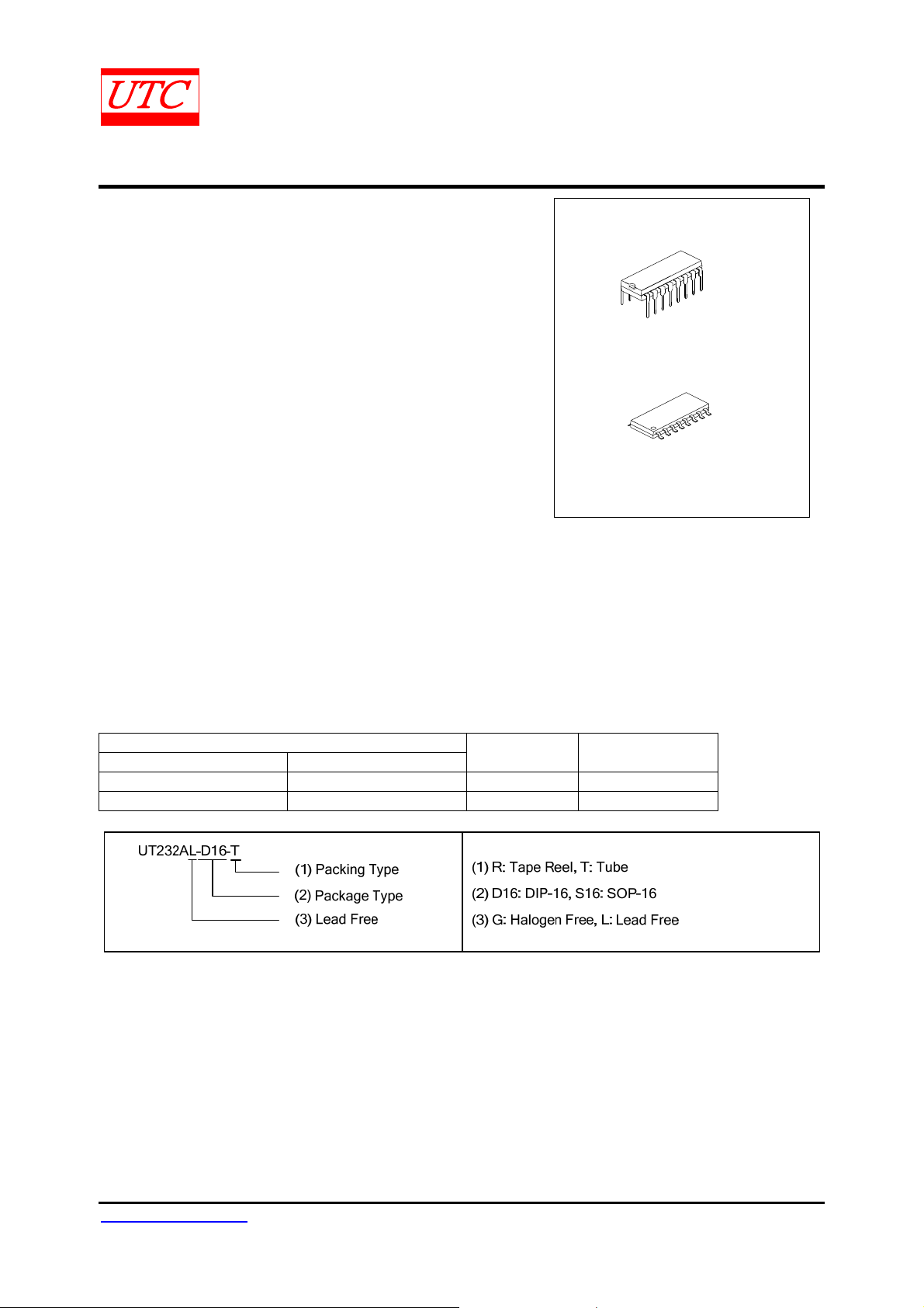
The UTC UT232A is available in DIP-16 package and SOP-16
package.
FEATURES
* Single power supply: 5V
* Low power supply current: 10mA
* Multiple drivers and receivers
* Receiver input levels:±30V
* 3-State outputs of TTL/CMOS receiver
* High output slew rate: 10V/µs under load
* High data rate: 120kbps under load
* Four external small charge pump capacitors: 0.1µF
DIP-16
SOP-16
Lead-free: UT232AL
Halogen-free: UT232AG
ORDERING INFORMATION
Ordering Number
Lead Free Halogen Free
UT232AL-D16-T UT232AG-D16-T DIP-16 Tube
UT232AL-S16-R UT232AG-S16-R SOP-16 Tape Reel
Package Packing
www.unisonic.com.tw 1 of 5
Copyright © 2010 Unisonic Technologies Co., Ltd QW-R502-272.d
Page 2
UT232A Preliminary CMOS
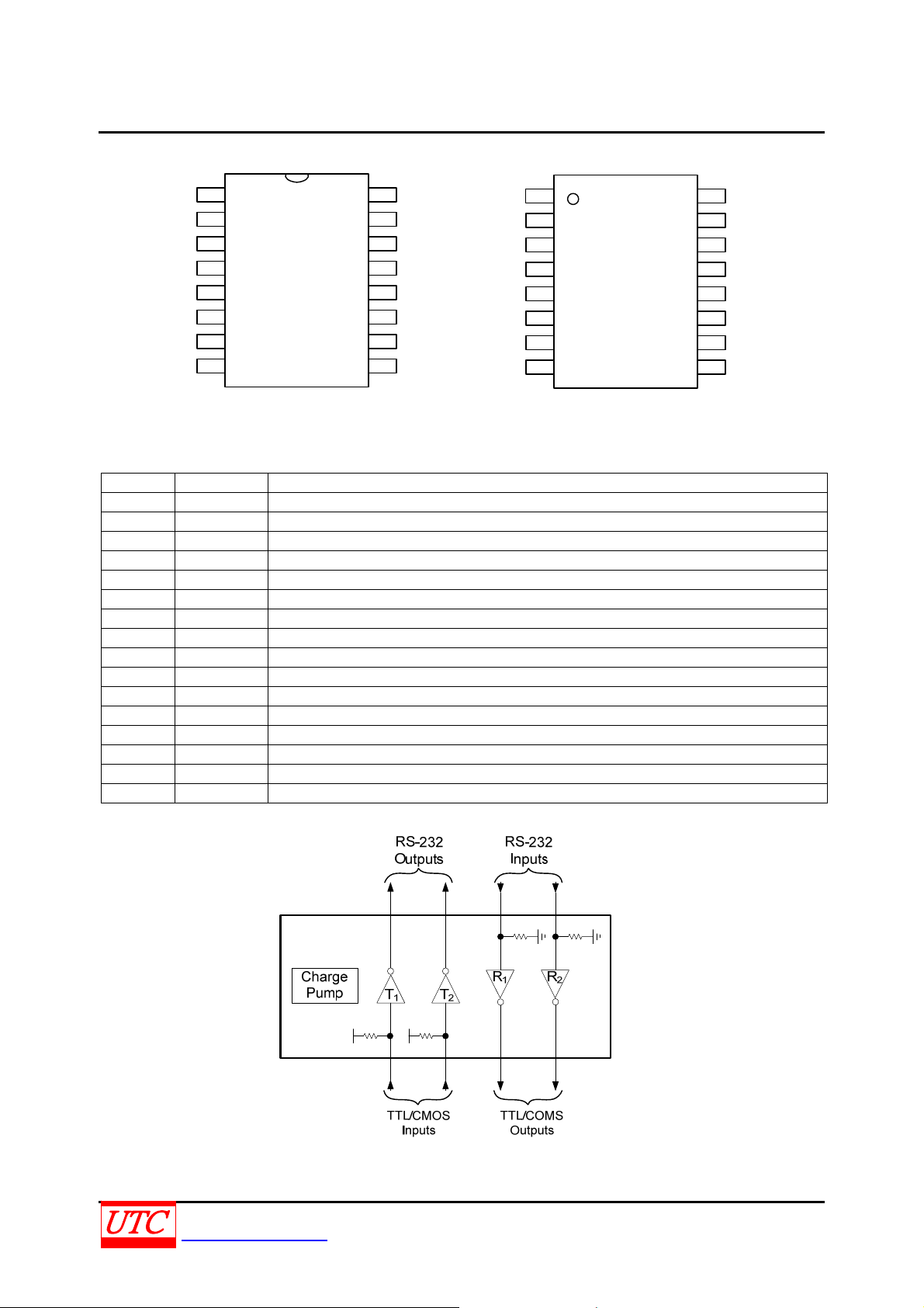
PIN CONFIGURATION
1
+
C
1
2
V+
-
C
3
1
4
C
+
T
C2-
V-
OUT
2
R
2
5
6
7
IN
89
2
DIP-16
PIN DESCRIPTION
PIN NO. PIN NAME DESCRIPTION
1 C1+
2 V+
3 C1-
Positive terminal of the voltage doubler Charge-Pump Capacitor
Positive voltage generated by the charge pump
Negative terminal of the voltage doubler Charge-Pump Capacitor
4 C2+ Positive terminal of inverting Charge-Pump Capacitor
5 C2- Negative terminal of inverting Charge-Pump Capacitor
6 v- Negative voltage generated by the charge pump
7 T2OUT
8 R2IN
9 R2OUT
10 T2IN
11 T1IN
12 R1OUT
13 R1IN
14 T1OUT
RS-232 Transmitter Outputs
RS-232 Receiver Inputs
TTL/CMOS Receiver Outputs
TTL/CMOS Transmitter Inputs
TTL/CMOS Transmitter Inputs
TTL/CMOS Receiver Outputs
RS-232 Receiver Inputs
RS-232 Transmitter Outputs
15 GND Ground
16 VCC
Power Supply
16
15
14
13
12
11
10
V
CC
GND
OUT
T
1
R
IN
1
R1OUT
IN
T
1
T
IN
2
OUT
R
2
1
+
T
C
C
C
C2-
V-
OUT
2
R
1
2
V+
-
3
1
4
+
2
SOP-16
5
6
7
IN
89
2
16
15
14
13
12
11
10
V
CC
GND
OUT
T
1
R
IN
1
R1OUT
IN
T
1
T
IN
2
R2OUT
UNISONIC TECHNOLOGIES CO., LTD 2 of 5
www.unisonic.com.tw QW-R502-272.d
Page 3
UT232A Preliminary CMOS
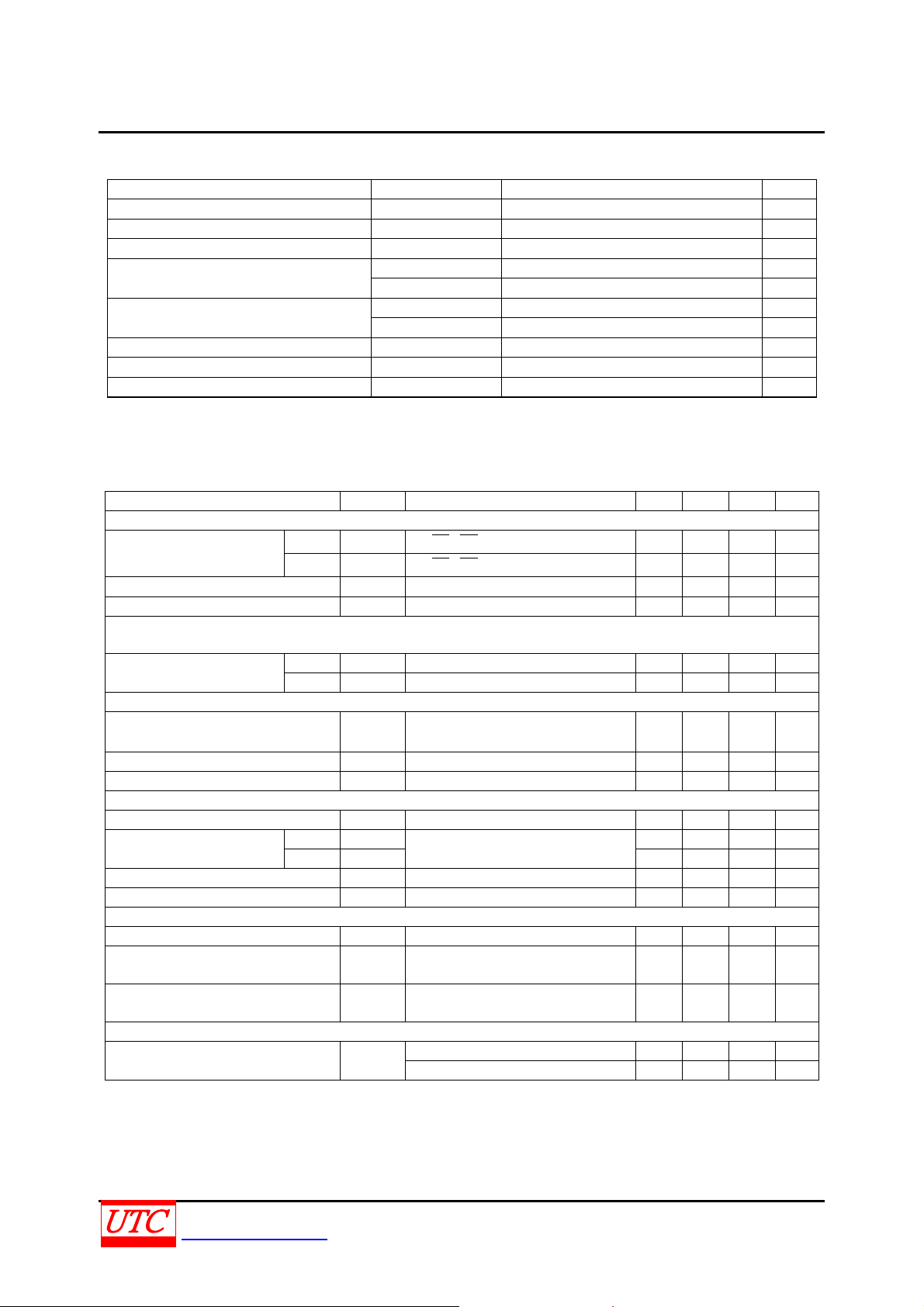
ABSOLUTE MAXIMUM RATINGS
PARAMETER SYMBOL RATINGS UNIT
Supply voltage range
Positive-output supply voltage range
Negative-output supply voltage range
Input Voltages
Output Voltages
Short Circuit Duration T
Power Dissipation PD 375 mW
Operating Temperature T
Note : Absolute maximum ratings are those values beyond which the device could be permanently damaged.
Absolute maximum ratings are stress ratings only and functional device operation is not implied.
ELECTRICAL CHARACTERISTICS
V
6 V
CC
+
V
(VCC-0.3) ~+13.2 V
-
V
13.2V V
TIN -0.3~(VCC+0.3) V
±30 V
R
IN
T
(V+, +0.3) ~(V-, -0.3) V
OUT
-0.3~(Vcc+0.3) V
R
OUT
Continuous
OUT
0 ~ +70 °С
OPR
(VCC=+5V±10%; 0.1µF charge pump capacitors; T
MIN
to T
unless otherwise specified.)
MAX
PARAMETER SYMBOL TEST CONDITIONS MIN TYP MAX UNIT
TTL INPUT
Logic Threshold
Low VTL
High V
TH
;EN,SD
T
IN
;EN,SD
T
IN
0.8 V
2.0 V
Logic Pull up Current ITH TIN=0V 15 200 µA
Maximum Data Rate CL=2500pF, RL=3kΩ 120 kps
TTL OUTPUT
TTL/CMOS Output Voltage
Low VOL I
High V
OH
=3.2mA; VCC=+5V 0.4 V
OUT
I
=-1.0mA 3.5 V
OUT
RS-232 OUTPUT
Output Voltage Swing V
All transmitter outputs loaded
O(SW)
With 3kΩ to Ground
Output Resistance RO VCC=0V; V
Output Short Circuit Current I
Infinite duration ±18 mA
O(SC)
=±2V 300 Ω
OUT
±5 ±9 V
RS-232 INPUT
Voltage Range V
Voltage Threshold
Low V
High V
Hysteresis V
-30 +30 V
I(SW)
THR(L)
VCC=5V, TA=+25°С
THR(H)
VCC=5V, TA=+25°С 0.2 0.5 1.0 V
HYS
0.8 1.2 V
1.7 2.4 V
Resistance RI TA=+25°С, -15V≤VIN≤+15V 3 5 8 kΩ
DYNAMIC CHARACTERISTICS
Propagation Delay, RS232 to TTL tPD 1.5 µs
Instantaneous Slew Rate SR
Transition Region Slew Rate SR
L
T
=+25°С
A
C
=2500pF, RL=3kΩ;measured from
L
+3V ~ -3V or -3V ~ +3V
30 V/µs
10 V/µs
C
=10pF, RL=3-7kΩ;
POWER REQUIREMENTS
VCC Power Supply Current ICC
No load, TA=+25°С; VCC=5V 10 15 mA
All transmitters R
=3kΩ;TA=+25°С 25 mA
L
UNISONIC TECHNOLOGIES CO., LTD 3 of 5
www.unisonic.com.tw QW-R502-272.d
Page 4
UT232A Preliminary CMOS
FUNCTION DESCRIPTION
Driver/Transmitter
The drivers are inverting transmitters, which accept TTL or CMOS inputs and output the RS-232 signals with an
inverted sense relative to the input logic levels. Typically the RS-232 output voltage swing is ±9V. Even under worst
case loading conditions of 3kOhms and 2500pF, the output is guaranteed to be ±5V, which is consistent with the
RS-232 standard specifications. The transmitter outputs are protected against infinite short-circuits to ground without
degradation in reliability.
The instantaneous slew rate of the transmitter output is internally limited to a maximum of 30V/µs. However, the
transition region slew rate of these enhanced products is typically 10V/µs. The smooth transition of the loaded output
from VOL to VOH clearly meets the monotonicity requirements.
Receivers
The receivers convert RS-232 input signals to inverted TTL signals. Since the input is usually from a transmission
line, where long cable lengths and system interference can degrade the signal, the inputs have a typical hysteresis
margin of 0.5V.
This ensures that the receiver is virtually immune to noisy transmission lines. The input thresholds are 0.8V
minimum and 2.4V maximum, again well within the ±3V RS-232 requirements. The receiver inputs are also protected
against voltages up to ±30V. Should an input be left unconnected, a 5kOhm pull down resistor to ground will commit
the output of the receiver to a high state.
In actual system applications, it is quite possible for signals to be applied to the receiver inputs before power is
applied to the receiver circuitry.
This occurs, for example, when a PC user attempts to print, only to realize the printer wasn’t turned on. In this
case an RS-232 signal from the PC will appear on the receiver input at the printer. When the printer power is turned
on, the receiver will operate normally. All of these enhanced devices are fully protected.
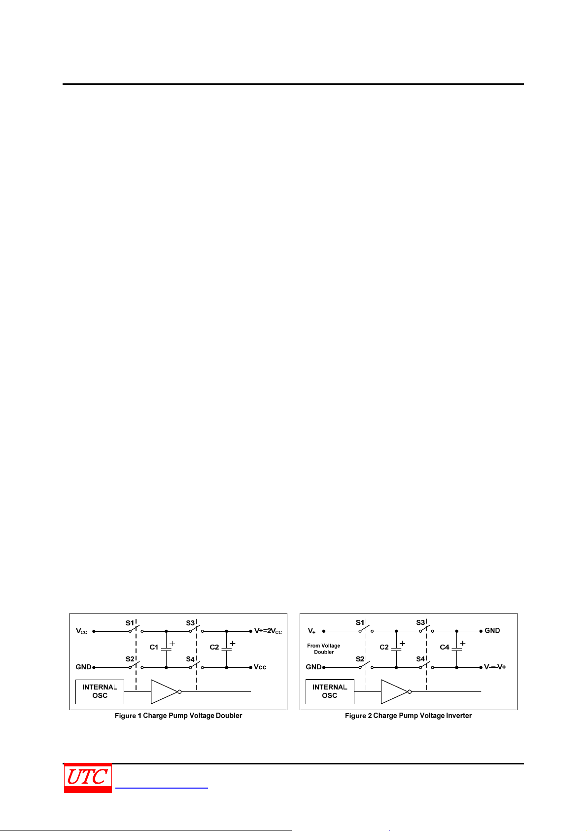
Charge Pump
The charge pump section of the these devices allows the circuit to operate from a single +5V±10% power supply
by generating the required operating voltages internal to the devices. The charge pump consists of a voltage doubler
and a voltage inverter. As shown in Figure 1, an internal oscillator triggers the charge accumulation and voltage
inversion. The voltage doubler momentarily stores a charge on capacitor C1 equal to V
During the next transition of the oscillator this charge is boot-strapped to transfer charge to capacitor C3. The voltage
across C3 is now from V
In the inverter section as shown in Figure 2, the voltage across C3 is transferred to C2 forcing a range of 0V to
V+ across C2. Boot-strapping of C2 will then transfer charge to C4 to generate V-. One of the significant
enhancements over previous products of this type is that the values of the capacitors are no longer critical and have
been decreased in size considerably to 0.1mF. Because the charge pump runs at a much higher frequency, the
0.1uF capacitors are sufficient to transfer and sustain charges to the two transmitters.
to V+.
CC
, referenced to ground.
CC
UNISONIC TECHNOLOGIES CO., LTD 4 of 5
www.unisonic.com.tw QW-R502-272.d
Page 5
UT232A Preliminary CMOS
APPLICATION INFORMATION
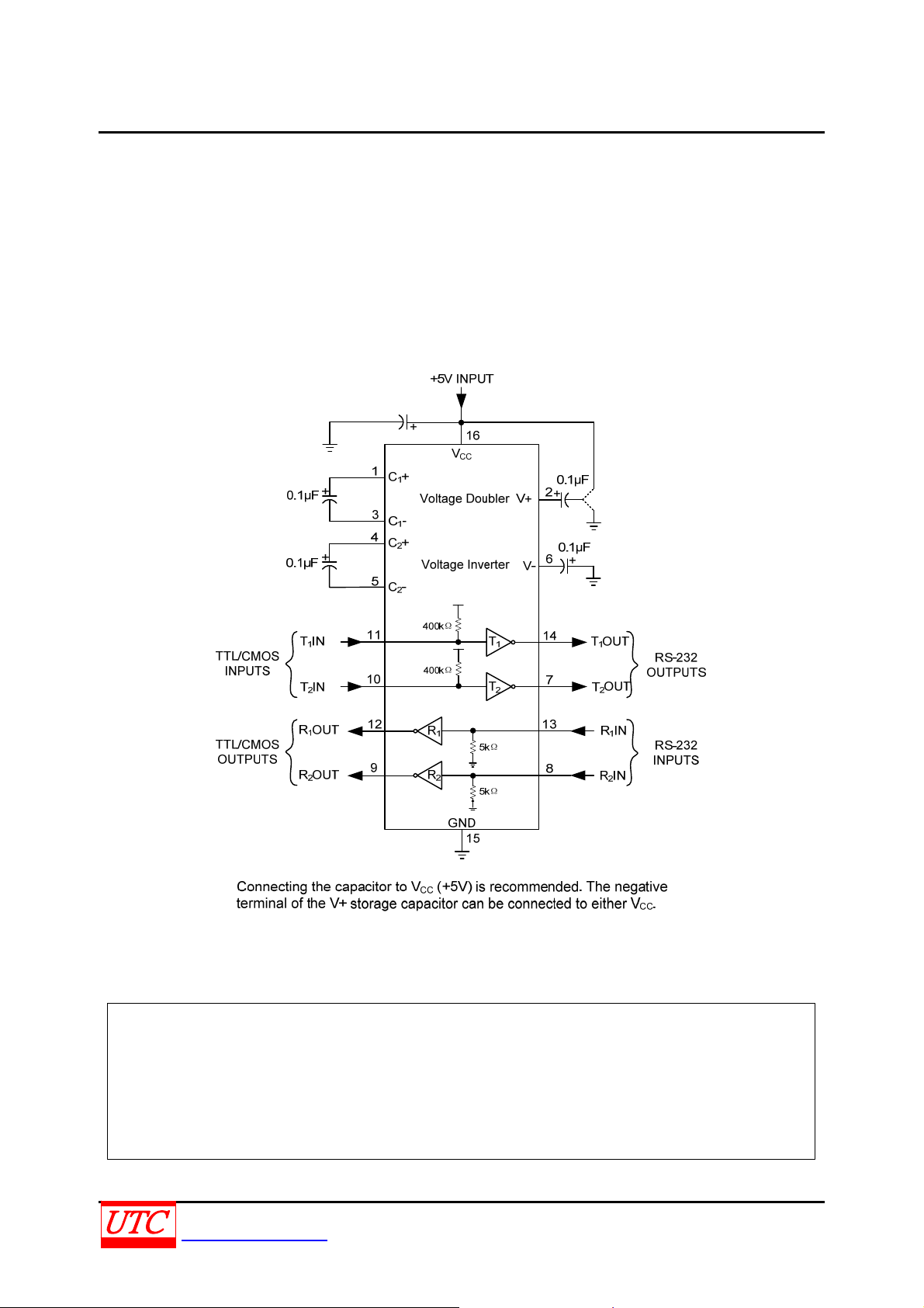
To operate from a single +5V supply, the UTC UT232A include charge pump voltage converters which can allow
it. To generate the RS-232 output levels these converters convert the +5V input power to the ±10V needed. The
current drain due to charge pump operation is considerably reduced, typically to 400µA with this power supplied
externally. The UTC UT232A can operate over the commercial, industrial and military temperature ranges.
Protection from Shorts to ±15V
Against shorts to ground, any other driver output, and V+ or V- the driver outputs are protected. If the outputs is
connected to voltages higher than ±15V inadvertently, then the external protection is recommended to be provided.
While voltages exceeding ±15V ,for protection, two back-to-back zener diodes which is connected from each output
to ground will clamp the outputs to an acceptable voltage level.
UTC assumes no responsibility for equipment failures that result from using products at values that
exceed, even momentarily, rated values (such as maximum ratings, operating condition ranges, or
other parameters) listed in products specifications of any and all UTC products described or contained
herein. UTC products are not designed for use in life support appliances, devices or systems where
malfunction of these products can be reasonably expected to result in personal injury. Reproduction in
whole or in part is prohibited without the prior written consent of the copyright owner. The information
presented in this document does not form part of any quotation or contract, is believed to be accurate
and reliable and may be changed without notice.
UNISONIC TECHNOLOGIES CO., LTD 5 of 5
www.unisonic.com.tw QW-R502-272.d
 Loading...