

Page 1

EVALUATION KIT AVAILABLE
Click here for production status of specific part numbers.
MAX17552/MAX17552A 60V, 100mA, Ultra-Small, High-Eciency,
Synchronous Step-Down DC-DC Converter
with 22µA No-Load Supply Current
General Description
The MAX17552/MAX17552A high-efficiency, high-voltage,
synchronous step-down DC-DC converters with integrated
MOSFETs operate over a 4V to 60V input voltage range.
The converters can deliver output current up to 100mA at
output voltages of 0.8V to 0.9 x VIN. The output voltage
is accurate to within ±1.75% over the -40°C to +125°C
temperature range.
The devices employ a peak-current-mode control
architecture with a MODE pin that can be used to operate
the device in pulse-width modulation (PWM) or pulsefrequency modulation (PFM) control schemes. PWM
operation provides constant frequency operation at all
loads and is useful in applications sensitive to variable
switching frequency. PFM operation disables negative
inductor current and additionally skips pulses at light
loads for high efficiency. The converters consume only
22µA of no-load supply current in PFM mode. The low-
resistance, on-chip MOSFETs ensure high efficiency at
full load and simplify PCB layout.
The devices offer programmable switching frequency to
optimize solution size and efficiency. Programmable softstart allows the user to reduce the inrush currents. During
overload, the MAX17552 implements a hysteretic cycleby-cycle peak-current-limit protection scheme, while the
MAX17552A implements a HICCUP-type overload protection scheme to protect the inductor and the internal FETs.
An EN/UVLO pin allows the user to turn on/off the device
at the desired input-voltage level. An open-drain RESET
pin allows output-voltage monitoring. The devices operate
over the -40°C to +125°C industrial temperature range
and is available in a compact 10-pin (3mm x 2mm) TDFN
and 10-pin (3mm x 3mm) μMAX® packages. Simulation
models are available.
Applications
● Industrial Sensors and Process Control
● 4mA–20mA Current-Loop Powered Sensors
● High-Voltage LDO Replacement
● Battery-Powered Equipment
● HVAC and Building Control
● General-Purpose Point of Load
Benets and Features
●
Eliminates External Components and Reduces Total Cost
• No Schottky—Synchronous Operation for High
Eciency and Reduced Cost
• Internal Compensation
• Fixed Internal 5.1ms or Programmable Soft-Start
• All-Ceramic Capacitors, Ultra-Compact Layout
● Reduces Number of DC-DC Regulators to Stock
• Wide 4V to 60V Input Voltage Range
• Adjustable 0.8V to 0.9 x VIN Output Voltages
• Delivers Up to 100mA Load Current
• 100kHz to 2.2MHz Adjustable Switching Frequency
Range with External Synchronization
• Congurable Between PFM and Forced-PWM
Modes
● Reduces Power Dissipation
• 22µA No Load Supply Current
• Peak Eciency > 90%
• PFM Feature for High Light-Load Eciency
• 1.2μA (typ) Shutdown Current
● Operates Reliably in Adverse Industrial Environments
• Peak Current-Limit Protection
● Built-In Output-Voltage Monitoring with Open-Drain
RESET Pin
• Programmable EN/UVLO Threshold
• Monotonic Startup into Prebiased Output
• Overtemperature Protection
• High Industrial -40°C to +125°C Ambient Operating
Temperature Range / -40°C to +150°C Junction
Temperature Range
Ordering Information appears at end of data sheet.
µMAX is a registered trademark of Maxim Integrated Products, Inc.
19-6903; Rev 5; 8/18
Page 2
MAX17552/MAX17552A 60V, 100mA, Ultra-Small, High-Eciency
Synchronous Step-Down DC-DC Converter
with 22µA No-Load Supply Current
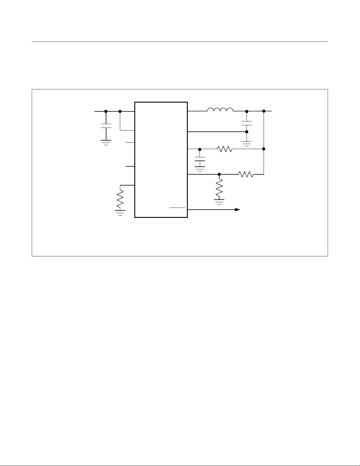
Typical Application Circuit—High-Eciency 5V, 100mA Regulator
V
IN
6V TO 60V
C
IN
1µF
191k
SWITCHING FREQUENCY = 220kHz
L1 COILCRAFT LPS5030-224M
C
C
MAX17552/
IN
LX
MAX17552A
EN/UVLO
SS
MODE
RT/SYNC
R3
Ω
MURATA 10µF/X7R/6.3V/1206 (GRM31CR70J106K)
OUT
MURATA 1µF/X7R/100V/1206 (GRM31CR72A105K)
IN
GND
V
OUT
FB
RESET
C1
0.22
220
µ
L1
µ
R4
22.1
F
H
C
10µF
Ω
R2
49.9k
OUT
Ω
R1
261k
V
OUT
5V, 100mA
Ω
www.maximintegrated.com
Maxim Integrated
│
2
Page 3
MAX17552/MAX17552A 60V, 100mA, Ultra-Small, High-Eciency
Synchronous Step-Down DC-DC Converter
with 22µA No-Load Supply Current
Absolute Maximum Ratings (Note 1)
IN, EN/UVLO, V
LX to GND ....................................................... -0.3V to IN +0.3V
RT/SYNC, SS, FB, MODE to GND .........................-0.3V to +6V
LX Total RMS Current ........................................................ ±1.6A
Output Short-Circuit Duration .................................... Continuous
Stresses beyond those listed under “Absolute Maximum Ratings” may cause permanent damage to the device. These are stress ratings only, and functional operation of the device at these
or any other conditions beyond those indicated in the operational sections of the specifications is not implied. Exposure to absolute maximum rating conditions for extended periods may affect
device reliability.
Note 1: Junction temperature greater than +125°C degrades operating lifetimes.
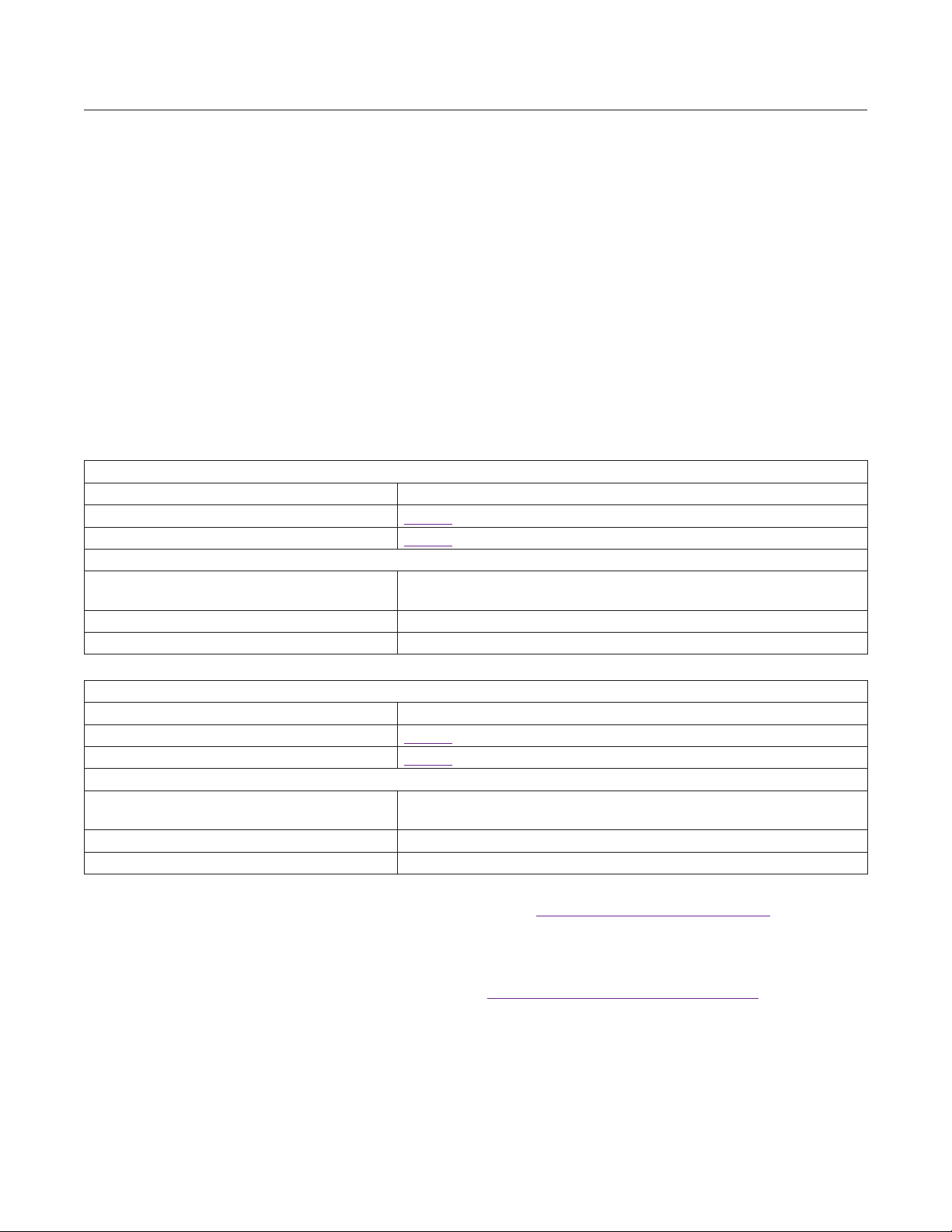
Package Information
PACKAGE TYPE: 10 TDFN
Package Code T1032N+1
Outline Number 21-0429
Land Pattern Number 90-0082
THERMAL RESISTANCE, FOUR-LAYER BOARD
Continuous Power Dissipation (TA = +70°C)
(derate 14.9mW/°C above +70°C)
Junction to Ambient (θJA) 67.3°C/W
Junction to Case (θJC) 18.2°C/W
, RESET to GND...................-0.3V to +70V
OUT
Junction Temperature ......................................................+150°C
Storage Temperature Range ............................ -65°C to +150°C
Lead Temperature (soldering, 10s) ................................. +300°C
Soldering Temperature (reflow) ....................................... +260°C
1188.7mW
PACKAGE TYPE: 10 µMAX
Package Code U10+5
Outline Number 21-0061
Land Pattern Number 90-0330
THERMAL RESISTANCE, FOUR-LAYER BOARD
Continuous Power Dissipation (TA = +70°C)
(derate 8.8mW/°C above +70°C)
Junction to Ambient (θJA) 113.1°C/W
Junction to Case (θJC) 42°C/W
For the latest package outline information and land patterns (footprints), go to www.maximintegrated.com/packages. Note that a “+”,
“#”, or “-” in the package code indicates RoHS status only. Package drawings may show a different suffix character, but the drawing
pertains to the package regardless of RoHS status.
Package thermal resistances were obtained using the method described in JEDEC specification JESD51-7, using a four-layer board.
For detailed information on package thermal considerations, refer to www.maximintegrated.com/thermal-tutorial.
707.3mW
www.maximintegrated.com
Maxim Integrated
│
3
Page 4
MAX17552/MAX17552A 60V, 100mA, Ultra-Small, High-Eciency
Synchronous Step-Down DC-DC Converter
with 22µA No-Load Supply Current
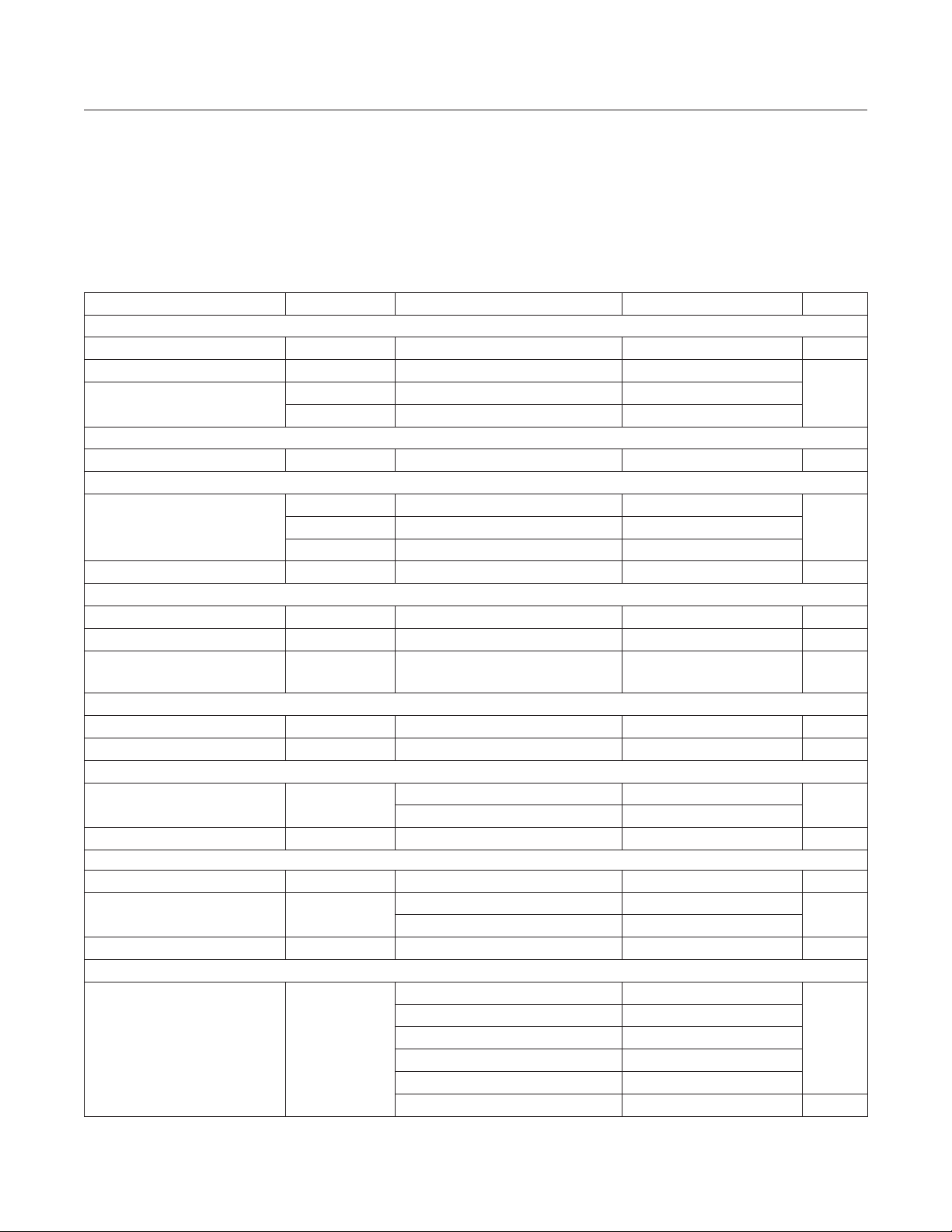
Electrical Characteristics
(VIN = 24V, V
TA = -40°C to +125°C, unless otherwise noted. Typical values are at TA = +25°C. All voltages are referenced to GND, unless otherwise
noted) (Note 2)
INPUT SUPPLY (IN)
Input Voltage Range V
Input Shutdown Current I
Input Supply Current
EXTERNAL BIAS (V
V
Switchover Threshold 2.96 3.05 3.12 V
OUT
ENABLE/UVLO (EN/UVLO)
EN/UVLO Threshold
EN/UVLO Leakage Current I
POWER MOSFETs
High-Side pMOS On-Resistance R
Low-Side nMOS On-Resistance R
LX Leakage Current I
SOFT-START (SS)
Soft-Start Time t
SS Charging Current I
FEEDBACK (FB)
FB Regulation Voltage V
FB Input Leakage Current I
CURRENT LIMIT
Peak Current-Limit Threshold I
Negative Current-Limit Threshold I
PFM Current Level I
OSCILLATOR (RT/SYNC)
Switching Frequency f
GND
= 0V, V
= 3.3V, VFB = 0.85V, V
VOUT
EN/UVLO
= 1.5V, RT/SYNC = 191kΩ, LX = SS = MODE = RESET = unconnected;
PARAMETER SYMBOL CONDITIONS MIN TYP MAX UNITS
4 60 V
µA
VV
-1 +1 µA
4.7 5 5.3 µA
V
185 210 235 mA
mA
OUT)
IN
IN-SH
I
Q-PFM
I
Q-PWM
V
ENR
ENF
V
EN-TRUESDVEN/UVLO
EN
DS-ONH
DS-ONL
LX-LKG
SS
SS
V
EN/UVLO
V
MODE
Normal switching mode, VIN = 24V 245 525 760
V
EN/UVLO
V
EN/UVLO
V
EN/UVLO
ILX = 0.1A (sourcing) 1.5 2.7 5.1 Ω
ILX = 0.1A (sinking) 0.8 1.4 2.6 Ω
VEN = 0V, TA = +25°C,
VLX = (V
SS = unconnected 4.4 5.1 5.8 ms
MODE = GND 0.786 0.8 0.814
FB-REG
FB
PEAK-LIMIT
SINK-LIMIT
PFM
MODE = unconnected 0.786 0.812 0.826
VFB = 1V, TA = 25°C -100 +100 nA
V
MODE
V
MODE
V
MODE
= 0V, TA = +25°C 0.67 1.2 2.25
= unconnected (Note 3) 18 32
rising 1.2 1.25 1.3
falling 1.1 1.15 1.2
falling, true shutdown 0.7
= 1.3V, TA = +25°C -100 +100 nA
+ 1V) to (VIN - 1V)
GND
= GND 79 105 130
= unconnected 0.01
= unconnected 50 72 90 mA
RRT = 422kΩ 90 100 111
RRT = 191kΩ 205 220 235
SW
RRT = 130kΩ 295 319 340
RRT = 69.8kΩ 540 592 638
kHz
RRT = 45.3kΩ 813 900 973
RRT = 19.1kΩ 1.86 2.08 2.3 MHz
www.maximintegrated.com
Maxim Integrated
│
4
Page 5
MAX17552/MAX17552A 60V, 100mA, Ultra-Small, High-Eciency
Synchronous Step-Down DC-DC Converter
with 22µA No-Load Supply Current
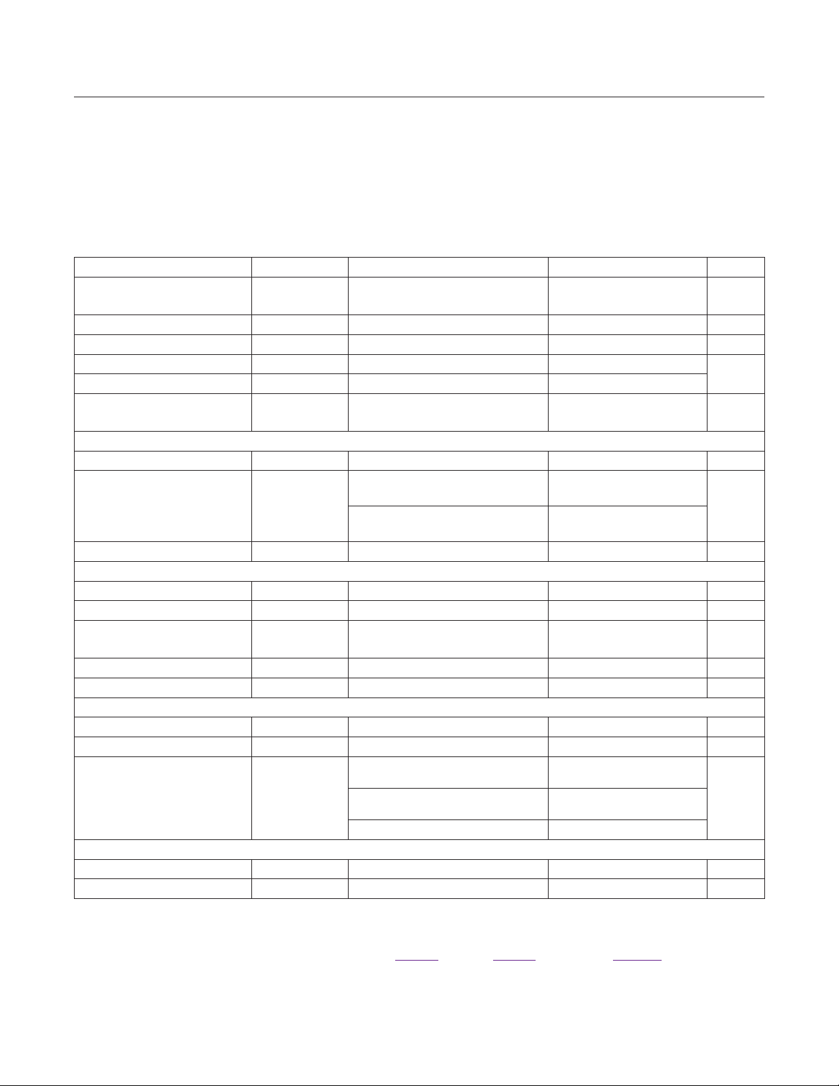
Electrical Characteristics (continued)
(VIN = 24V, V
TA = -40°C to +125°C, unless otherwise noted. Typical values are at TA = +25°C. All voltages are referenced to GND, unless otherwise
noted) (Note 2)
Switching Frequency Adjustable
Range
SYNC Input Frequency 1.1 x f
SYNC Pulse Minimum O-Time 40 ns
SYNC Rising Threshold V
Hysteresis V
Number of SYNC Pulses to
Enable Synchronization
TIMING
Minimum On-Time t
Maximum Duty Cycle D
Hiccup Timeout MAX17552A 51 ms
RESET
FB Threshold for RESET Rising V
FB Threshold for RESET Falling V
RESET Delay after FB Reaches
95% Regulation
RESET Output Level Low I
RESET Output Leakage Current VFB = 1.01 x V
MODE
MODE PFM Threshold V
MODE Hysteresis V
MODE Internal Pullup Resistor
THERMAL SHUTDOWN
Thermal-Shutdown Threshold Temperature rising 160 °C
Thermal-Shutdown Hysteresis 20 °C
Note 2: Limits are 100% tested at TA = +25°C. Limits over the operating temperature range and relevant supply voltage range are
guaranteed by design and characterization.
Note 3: Actual I
example, I
GND
= 0V, V
= 3.3V, VFB = 0.85V, V
VOUT
EN/UVLO
= 1.5V, RT/SYNC = 191kΩ, LX = SS = MODE = RESET = unconnected;
PARAMETER SYMBOL CONDITIONS MIN TYP MAX UNITS
See the Switching Frequency (RT/
SYNC) section for details
SYNC-H
SYNC-HYS
100 2200 kHz
SW
2200 kHz
1 1.22 1.44
0.115 0.18 0.265
V
1 Cycles
ON-MIN
MAX
FB-OKR
FB-OKF
fSW ≤ 600kHz,
VFB = 0.98 x V
FB-REG
fSW > 600kHz,
VFB = 0.98 x V
FB-REG
VFB rising 93 95 97 %
VFB falling 90 92 94 %
46 82 128 ns
90 94 98
%
87 92
2.1 ms
= 1mA 0.23 V
RESET
FB-REG
MODE-PFM
MODE-HYS
V
= unconnected
MODE
(MAX17552)
V
= unconnected
MODE
(MAX17552A)
V
= GND 1390
MODE
in the application circuit is higher due to additional current in the output voltage feedback resistor divider. For
Q-PFM
(MODE = unconnected) = 26µA for Figure 6, 22µA for Figure 7, and 78µA for Figure 11.
Q-PFM
TA = +25°C 1 µA
,
1 1.22 1.44 V
0.19 V
235
123
kΩ
www.maximintegrated.com
Maxim Integrated
│
5
Page 6
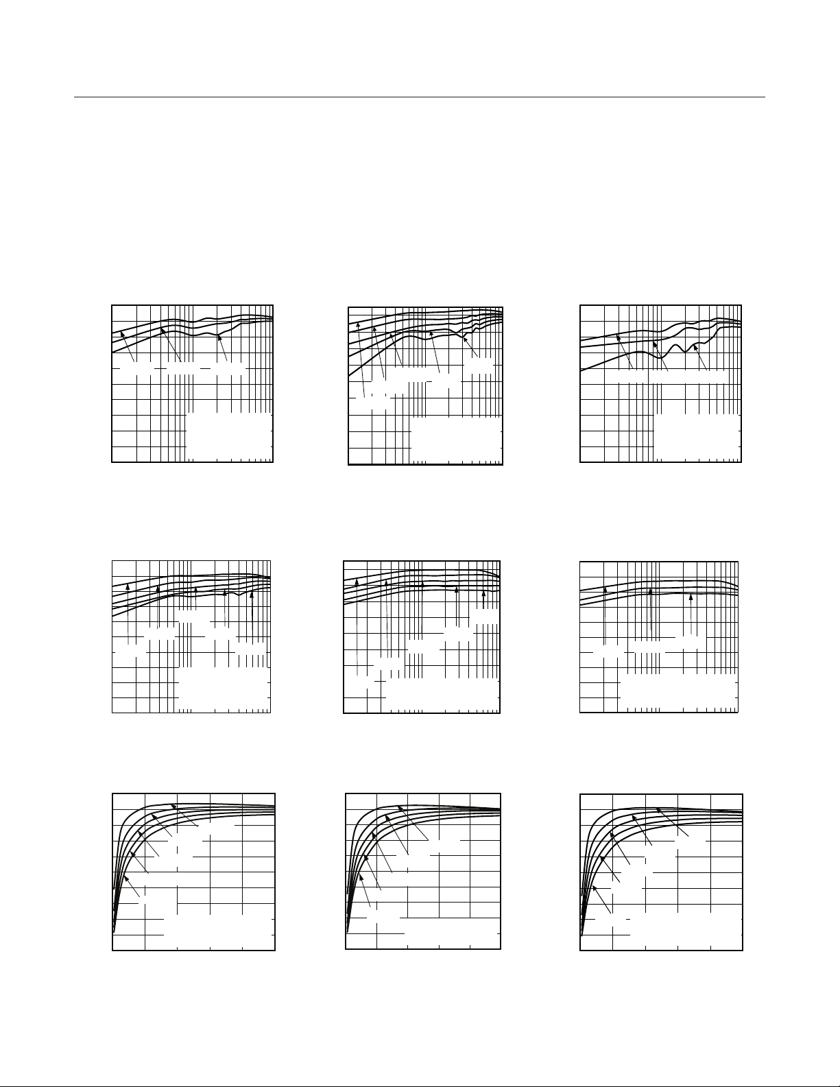
(MAX17552)
(MAX17552A)
EFFICIENCY vs. LOAD CURRENT
(MAX17552A)
(MAX17552A)
(MAX17552A)
MAX17552/MAX17552A 60V, 100mA, Ultra-Small, High-Eciency
Synchronous Step-Down DC-DC Converter
with 22µA No-Load Supply Current
Typical Operating Characteristics
(VIN = 24V, V
GND
= 0V, V
OUT
= 3.3V, V
EN/UVLO
= 1.5V, RT/SYNC = 191kΩ, CIN = 1μF, TA = +25°C unless otherwise noted.)
EFFICIENCY vs.
100
90
80
70
60
VIN= 12V
50
40
EFFICIENCY (%)
30
20
10
0
1 10 100
100
90
80
70
60
50
40
EFFICIENCY (%)
30
20
10
0
VIN= 24V
VIN= 12V
1 10 100
LOAD CURRENT
VIN= 24V
FIGURE 6 APPLICATION
CIRCUIT, PFM MODE
fSW = 220kHz (RRT = 191k)
LOAD CURRENT (mA)
V
= 36V
IN
VIN= 48V
FIGURE 7 APPLICATION
CIRCUIT, PFM MODE
F
= 220kHz(RRT= 191k)
SW
LOAD CURRENT (mA)
VIN= 36V
V
V
VIN= 60V
= 3.3V
OUT
toc1
90
80
70
60
50
40
EFFICIENCY (%)
30
= 5V
OUT
20
10
0
1 10 100
VIN= 24V
VIN= 12V
VIN= 36V
VIN= 48V
FIGURE 6 APPLICATION
CIRCUIT, PFM MODE
f
= 220kHz (RRT = 191k)
SW
VIN= 60V
V
OUT
toc2
EFFICIENCY (%)
= 5V
EFFICIENCY vs. LOAD CURRENT
EFFICIENCY vs.
100
90
80
70
60
50
40
30
20
10
VIN= 12V
0
1 10 100
LOAD CURRENT (mA)
EFFICIENCY vs LOAD CURRENT
toc4
90
80
70
60
50
40
EFFICIENCY (%)
30
20
10
0
VIN= 24V
VIN= 12V
1 10 100
FIGURE 6 APPLICATION CIRCUIT,
LOAD CURRENT (mA)
VIN= 48V
VIN= 36V
PFM MODE, V
= 600kHz (RRT= 69.8k)
F
SW
VIN= 60V
= 5V
OUT
toc5
EFFICIENCY vs. LOAD CURRENT
100
90
80
70
60
50
40
VIN= 12V
EFFICIENCY (%)
30
20
10
0
1 10 100
LOAD CURRENT
(MAX17552)
VIN= 24V
VIN= 36V
FIGURE 7 APPLICATION
CIRCUIT, PFM MODE
V
= 3.3V
VIN= 36V
OUT
OUT
= 3.3V
fSW= 220kHz (RRT= 191k)
LOAD CURRENT (mA)
VIN= 24V
FIGURE 7 APPLICATION CIRCUIT,
PFM MODE, V
= 600kHz (RRT= 69.8k)
F
SW
LOAD CURRENT (mA)
toc3
toc6
100
90
80
70
60
50
40
EFFICIENCY (%)
30
20
10
0
020406080100
www.maximintegrated.com
EFFICIENCY vs.
LOAD CURRENT
(MAX17552)
VIN=24V
VIN=36V
VIN=48V
VIN=60V
FIGURE 6APPLICATION CIRCUIT,
F
SW
LOAD CURRENT(mA)
VIN=12V
PWM MODE, V
= 220kHz (RRT = 191k)
OUT
= 5V
EFFICIENCY vs.LOADCURRENT
toc7
100
(MAX17552A)
90
80
70
60
50
40
EFFICIENCY (%)
30
20
VIN=36V
VIN=48V
VIN=60V
10
0
020406080100
VIN=12V
VIN=24V
FIGURE 6APPLICATION CIRCUIT,
PWM MODE, V
F
= 220kHz (RRT = 191k)
SW
toc8
EFFICIENCY (%)
= 5V
OUT
EFFICIENCY
100
90
80
70
60
50
40
30
20
VIN= 60V
10
0
0 20 40 60 80 100
LOAD CURRENT(mA)
VS.
LOAD CURRENT
(MAX17552)
VIN= 12V
VIN= 24V
VIN= 36V
VIN= 48V
FIGURE 7 APPLICATION CIRCUIT,
PWM MODE, V
= 220kHz (RRT= 191k)
F
SW
LOAD CURRENT (mA)
Maxim Integrated
OUT
= 3.3V
toc9
│
6
Page 7
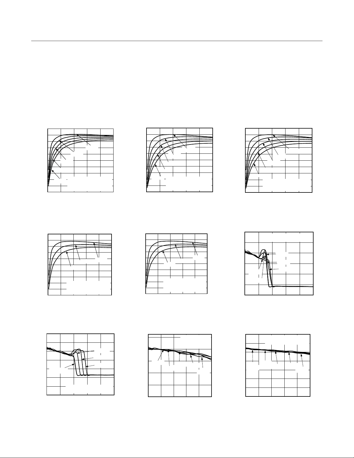
0
10
20
30
40
50
60
70
80
90
100
0 20 40 60 80 100
EFFICIENCY
(%)
LOAD CURRENT (mA)
EFFICIENCYVS. LOAD CURRENT
(MAX17552A)
toc14
VIN= 36V
VIN= 12V
VIN= 24V
FIGURE 7 APPLICATION CIRCUIT,
PWM MODE, V
OUT
= 3.3V
FSW= 600kHz (RRT= 69.8k)
OUTPUT VOLTAGE (V)
MAX17552/MAX17552A 60V, 100mA, Ultra-Small, High-Eciency
Synchronous Step-Down DC-DC Converter
with 22µA No-Load Supply Current
Typical Operating Characteristics (continued)
(VIN = 24V, V
GND
= 0V, V
OUT
= 3.3V, V
EN/UVLO
= 1.5V, RT/SYNC = 191kΩ, CIN = 1μF, TA = +25°C unless otherwise noted.)
EFFICIENCY VS. LOAD CURRENT
100
90
80
70
60
50
40
EFFICIENCY (%)
30
20
10
0
0 20 40 6 0 80 100
100
90
80
70
60
50
40
EFFICIENCY (%)
30
20
10
0
0 20 40 60 80 100
(MAX17552A)
VIN= 12V
VIN= 24V
VIN= 36V
VIN= 48V
FIGURE 7 APPLICATION CIRCUIT,
VIN= 60V
EFFICIENCY VS. LOAD CURRENT
PWM MODE, V
= 220kHz (RRT= 191k)
F
SW
LOAD CURRENT (mA)
(MAX17552)
VIN= 24V
VIN= 36V
FIGURE 7 APPLICATION CIRCUIT,
F
LOAD CURRENT (mA)
VIN= 12V
PWM MODE, V
= 600kHz (RRT= 69.8k)
SW
EFFICIENCY vs. LOAD CURRENT
toc10
= 3.3V
OUT
toc13
= 3.3V
OUT
100
90
80
70
60
50
40
EFFICIENCY (%)
30
VIN= 60V
20
10
0
0 20 40 60 80 100
(MAX17552)
VIN= 12V
VIN= 24V
VIN= 36V
VIN= 48V
FIGURE 6 APPLICATION CIRCUIT,
PWM MODE, V
F
= 600kHz (RRT= 69.8k)
SW
LOAD CURRENT (mA)
OUT
toc11
= 5V
OUTPUT VOLTAGE (V)
EFFICIENCY vs. LOAD CURRENT
100
90
80
70
60
50
40
EFFICIENCY (%)
30
20
10
0
0 20 40 60 80 100
OUTPUT VOLTAGE vs. LOAD CURRENT
5.10
5.07
5.04
5.01
VIN= 12V
4.98
4.95
4.92
0 20 40 60 80 100
(MAX17552A)
VIN= 24V
VIN= 36V
VIN= 48V
VIN= 60V
FIGURE 6 APPLICATION CIRCUIT,
PWM MODE, V
= 600kHz (RRT= 69.8k)
F
SW
LOAD CURRENT (mA)
FIGURE 6 APPLICATION
CIRCUIT, PFM MODE
VIN= 36V
VIN= 48V
VIN= 60V
VIN= 24V
LOAD CURRENT (mA)
VIN= 12V
OUT
toc12
= 5V
toc15
OUTPUT VOLTAGE vs. LOAD CURRENT
3.42
3.40
3.38
3.36
3.34
VIN= 12V,24V
3.32
OUTPUT VOLTAGE (V)
3.30
3.28
0 20 40 60 80 100
www.maximintegrated.com
FIGURE 7 APPLICATION CIRCUIT,
LOAD CURRENT (mA)
VIN= 36V
VIN= 48V
VIN= 60V
PFM MODE
toc16
OUTPUT VOLTAGE vs. LOAD CURRENT
4.947
4.945
4.943
VIN= 12V
4.941
4.939
4.937
0 20 40 60 80 100
FIGURE6 APPLICATION
CIRCUIT, PWM MODE
VIN= 36V
VIN= 24V
LOAD CURRENT (mA)
VIN= 48V
toc17
VIN= 60V
OUTPUT VOLTAGE vs. LOAD CURRENT
3.330
3.328
3.326
3.324
VIN= 12V
3.322
3.320
OUTPUT VOLTAGE (V)
3.318
3.316
0 20 40 60 80 100
FIGURE 7 APPLICATION CIRCUIT,
VIN= 24V
LOAD CURRENT (mA)
VIN= 36V
VIN= 48V
Maxim Integrated
PWM MODE
VIN= 60V
toc18
│
7
Page 8
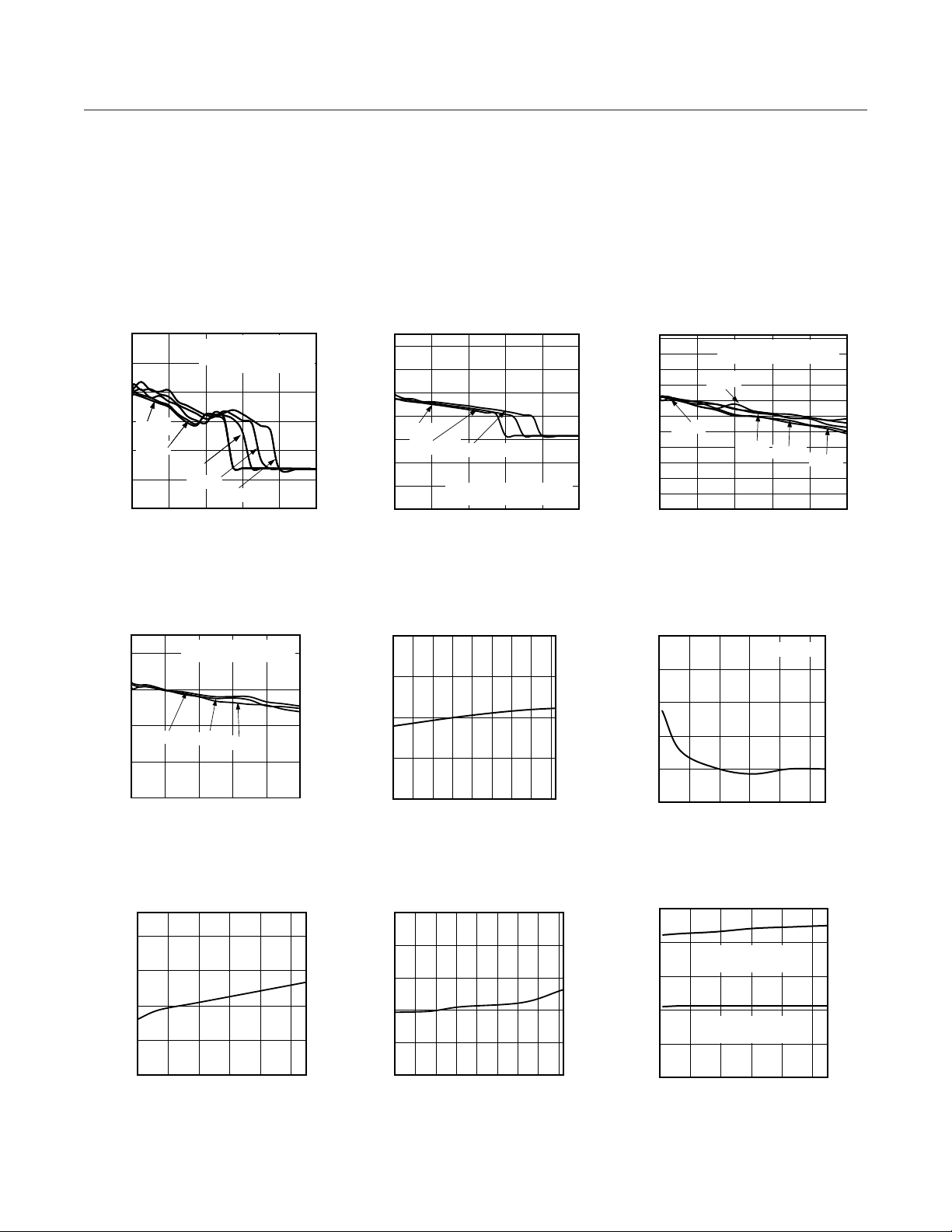
OUTPUT VOLTAGE (V)
FEEDBACK VOLTAGE (V)
SHUTDOWN CURRENT (µA)
MAX17552/MAX17552A 60V, 100mA, Ultra-Small, High-Eciency
Synchronous Step-Down DC-DC Converter
with 22µA No-Load Supply Current
Typical Operating Characteristics (continued)
(VIN = 24V, V
GND
= 0V, V
OUT
= 3.3V, V
EN/UVLO
= 1.5V, RT/SYNC = 191kΩ, CIN = 1μF, TA = +25°C unless otherwise noted.)
OUTPUT VOLTAGE vs. LOAD CURRENT
5.14
5.10
5.06
5.02
VIN=12V
VIN= 12V
VIN=24V
VIN= 24V
4.98
OUTPUT VOLTAGE (V)
4.94
4.90
0 20 40 60 80 100
FIGURE 8 APPLICATION
VIN=36V
VIN= 36V
VIN= 48V
VIN= 60V
LOAD CURRENT (mA)
FIGURE8 APPLICATION
CIRCUIT, PFM MODE
CIRCUIT, PFM MODE
OUTPUT VOLTAGE vs. LOAD CURRENT
3.329
3.327
3.325
3.323
OUTPUT VOLTAGE (V)
3.321
0 20 40 60 80 100
FIGURE 9 APPLICATION CIRCUIT,
VIN= 12V
VIN= 24V
LOAD CURRENT (mA)
VIN= 36V
PWM MODE
toc19
toc22
3.48
3.44
3.40
3.36
VIN= 12V
3.32
3.28
OUTPUT VOLTAGE (V)
3.24
3.20
0.82
0.81
0.80
0.79
0.78
VIN= 24V
0 20 40 60 80 100
-40 -20 0 20 40 60 80 100 120
VIN= 36V
FIGURE 9 APPLICATION CIRCUIT,
LOAD CURRENT (mA)
FEEDBACK VOLTAGE
VS. TEMPERATURE
TEMPERATURE (°C)
PFM MODE
OUTPUT VOLTAGE vs. LOAD CURRENT
toc20
toc23
OUTPUT VOLTAGE vs. LOAD CURRENT
4.960
4.959
4.958
4.957
4.956
4.955
4.954
4.953
4.952
4.951
4.950
4.949
0 20 40 60 80 100
100
80
60
40
20
NO LOAD SUPPLY CURRENT (µA)
0
5 15 25 35 45 55
FIGURE 8 APPLICATION CIRCUIT,
VIN= 24V
VIN= 12V
VIN= 36V
LOAD CURRENT (mA)
NO LOAD SUPPLY CURRENT
vs. INPUT VOLTAGE
INPUT VOLTAGE (V)
VIN= 48V
PFM MODE
toc21
PWM MODE
VIN= 60V
toc24
SHUTDOWN CURRENT
vs. INPUT VOLTAGE
4.0
2.5
1.0
SHUTDOWN CURRENT (µA)
-0.5
-2.0
5 15 25 35 45 55
INPUT VOLTAGE (V)
toc25
2.0
1.7
1.4
1.1
0.8
0.5
SHUTDOWN CURRENT
vs. TEMPERATURE
-40 -20 0 20 40 60 80 100 120
TEMPERATURE (°C)
toc26
250
200
150
100
50
SWITCH CURRENT LIMIT (mA)
0
www.maximintegrated.com
SWITCH CURRENT LIMIT
vs. INPUT VOLTAGE
SWITCH PEAK
CURRENT LIMIT
SWITCH NEGATIVE
CURRENT LIMIT
5 15 25 35 45 55
INPUT VOLTAGE (V)
Maxim Integrated
toc27
│
8
Page 9
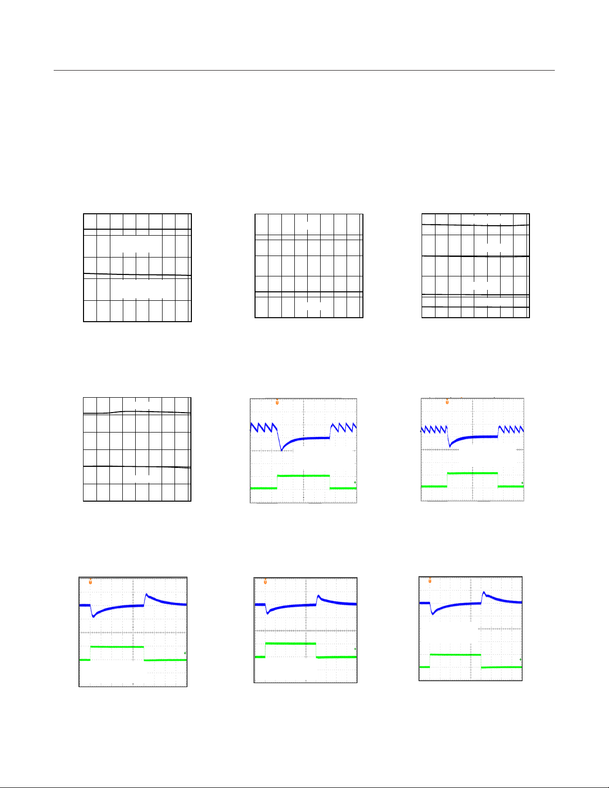
SWITCH CURRENT LIMIT (mA)
V
(
LOAD TRANSIENT RESPONSE
STEPPED FROM 50mA TO 100mA)
EN/UVLO THRESHOLD VOLTAGE (V)
V
(
LOAD TRANSIENT RESPONSE,
FROM 5mA to 50mA)
V
(
LOAD TRANSIENT RESPONSE
STEPPED FROM 50mA TO 100mA)
V
(
LOAD TRANSIENT RESPONSE
FROM 5mA to 50mA)
V
(
LOAD TRANSIENT RESPONSE
FROM NO-LOAD TO 50mA)
MAX17552/MAX17552A 60V, 100mA, Ultra-Small, High-Eciency
Synchronous Step-Down DC-DC Converter
with 22µA No-Load Supply Current
Typical Operating Characteristics (continued)
(VIN = 24V, V
GND
= 0V, V
OUT
= 3.3V, V
EN/UVLO
= 1.5V, RT/SYNC = 191kΩ, CIN = 1μF, TA = +25°C unless otherwise noted.)
SWITCH CURRENT LIMIT
250
200
150
100
50
0
-40 -20 0 20 40 60 80 100 120
96
95
94
93
92
RESET THRESHOLD (%)
91
90
-40 -20 0 20 40 60 80 100 120
vs. TEMPERATURE
SWITCH PEAK
CURRENT LIMIT
SWITCH NEGATIVE
CURRENT LIMIT
TEMPERATURE (°C)
RESET THRESHOLD
vs. TEMPERATURE
RISING
FALLING
TEMPERATURE (°C)
toc28
toc31
EN/UVLO THRESHOLD VOLTAGE
1.30
1.26
1.22
1.18
1.14
1.10
-40 -20 0 20 40 60 80 100 120
vs. TEMPERATURE
RISING
FALLING
TEMPERATURE (°C)
PFM MODE (LOAD CURRENT STEPPED
OUT
AC)
FIGURE6
APPLICATION
FIGURE 6
CIRCUIT
APPLICATION CIRCUIT
V
I
OUT
200µs/div
V
= 5V
OUT
SWITCHING FREQUENCY
toc29
1000
)
z
800
600
400
SWITCHING FREQUENCY (KH
200
0
-40 -20 0 20 40 60 80 100 120
vs. TEMPERATURE
RT= 45.3kΩ
RT= 69.8kΩ
RT= 191kΩ
RT= 422kΩ
TEMPERATURE (°C)
toc30
PFM MODE (LOAD CURRENT STEPPED
toc32
OUT
100mV/div
=5V
OUT
50mA/div
AC)
I
APPLICATION
FIGURE 7
APPLICATION CIRCUIT
= 3.3V
V
OUT
OUT
200µs/div
FIGURE7
CIRCUIT
V
=3.3V
OUT
toc33
100mV/div
50mA/div
PFM OR PWM MODE (LOAD CURRENT
OUT
AC)
I
OUT
www.maximintegrated.com
FIGURE 6
APPLICATION CIRCUIT
V
= 5V
OUT
100µs/div
toc34
100mV/div
50mA/div
PFM OR PWM MODE (LOAD CURRENT
OUT
AC)
I
OUT
FIGURE 7
APPLICATION CIRCUIT
V
= 3.3V
OUT
100µs/div
toc35
100mV/div
50mA/div
PWM MODE (LOAD CURRENT STEPPED
OUT
AC)
FIGURE 6
APPLICATION CIRCUIT
V
= 5V
OUT
I
OUT
100µs/div
Maxim Integrated
toc36
100mV/div
50mA/div
│
9
Page 10
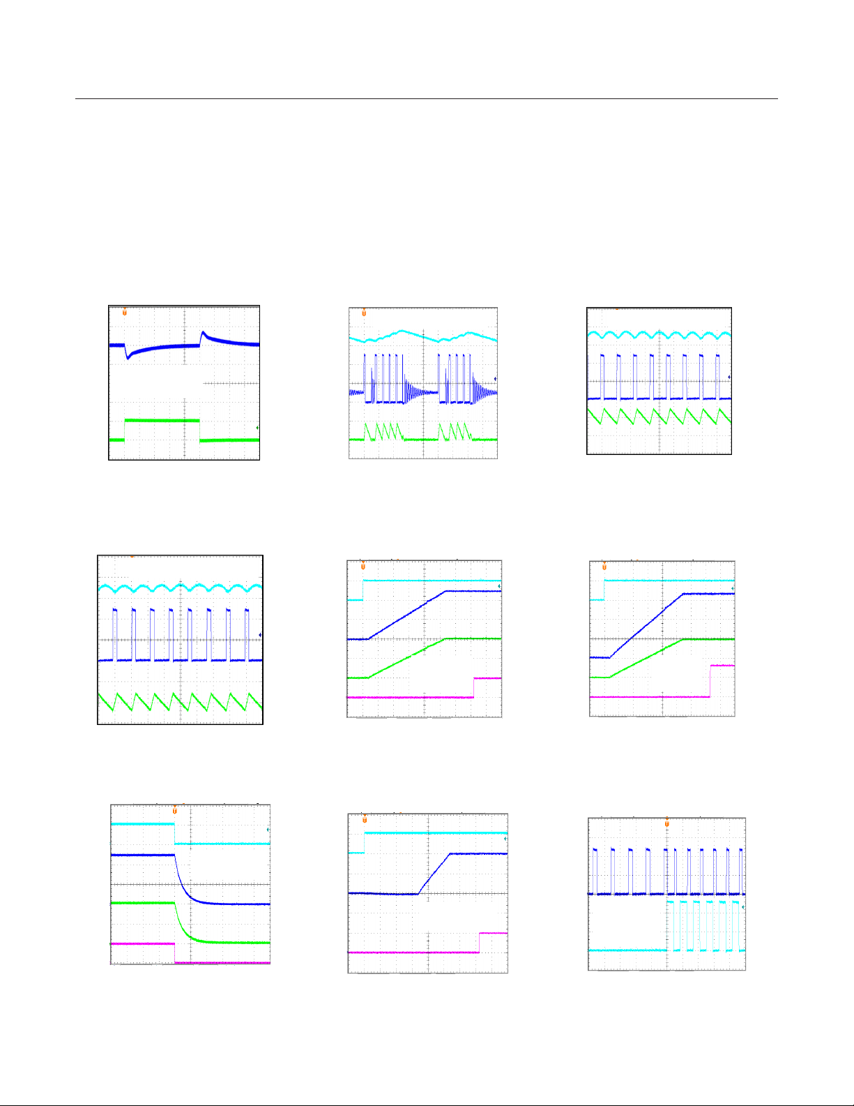
V
(
LOAD TRANSIENT RESPONSE
FROM NO-LOAD TO 50mA)
2V/div
5V/div
toc43
2ms/div
V
EN/UVLO
V
OUT
50mA/div
5V/div
SHUTDOWN WITH ENABLE
V
RESET
I
OUT
FIGURE 6
APPLICATION CIRCUIT
V
OUT
= 5V
V
(
(PFM MODE)
LX
V
EN/UVLO
V
T
(AC)
(PWM OR PFM MODE)
LX
V
RT/SYNC
V
(
LX
2V/div
5V/div
toc41
1ms/div
V
EN/UVLO
V
OUT
50mA/div
5V/div
SOFT START
I
OUT
V
RESET
FIGURE 6
APPLICATION
CIRCUIT
V
OUT
= 5V
V
EN/UVLO
MAX17552/MAX17552A 60V, 100mA, Ultra-Small, High-Eciency
Synchronous Step-Down DC-DC Converter
with 22µA No-Load Supply Current
Typical Operating Characteristics (continued)
(VIN = 24V, V
GND
= 0V, V
OUT
= 3.3V, V
EN/UVLO
= 1.5V, RT/SYNC = 191kΩ, CIN = 1μF, TA = +25°C unless otherwise noted.)
PWM MODE (LOAD CURRENT STEPPED
OUT
AC)
FIGURE 7
APPLICATION CIRCUIT
V
= 3.3V
OUT
I
OUT
100µs/div
NO LOAD SWITCHING WAVEFORMS
(PWM MODE)
FIGURE 6 APPLICATION CIRCUIT
V
= 5V
OUT
4µs/div
AC)
OUT
I
LX
toc37
toc40
100mV/
div
50mA/div
20mV/div
10V/div
100mA/div
AC)
SWITCHING WAVEFORMS
FIGURE 6 APPLICATION CIRCUIT
V
= 5V,LOAD = 20mA
OUT
OUT
I
LX
10µs/div
toc38
100mV/div
10V/div
100mA/div
FULL LOAD-SWITCHING WAVEFORMS
FIGURE 6 APPLICATION CIRCUIT
V
= 5V, LOAD = 100mA
OU
I
LX
OUT
4µs/div
SOFT START
V
V
I
RESET
OUT
OUT
FIGURE 7
APPLICATION
CIRCUIT
V
OUT
1ms/div
toc39
20mV/div
10V/div
100mA/div
toc42
5V/div
1V/div
50mA/div
2V/div
= 3.3V
www.maximintegrated.com
V
SOFT START WITH 3V PREBIAS
V
OUT
RESET
FIGURE 6
APPLICATION CIRCUIT
NO LOAD
PWM MODE
1ms/div
toc44
5V/div
1V/div
5V/div
EXTERNAL SYNCHRONIZATION WITH
300kHz CLOCK FREQUENCY
V
LX
FIGURE 6
APPLICATION
CIRCUIT
100mA LOAD
PWM MODE
4µs/div
Maxim Integrated
toc45
10V/div
2V/div
│
10
Page 11
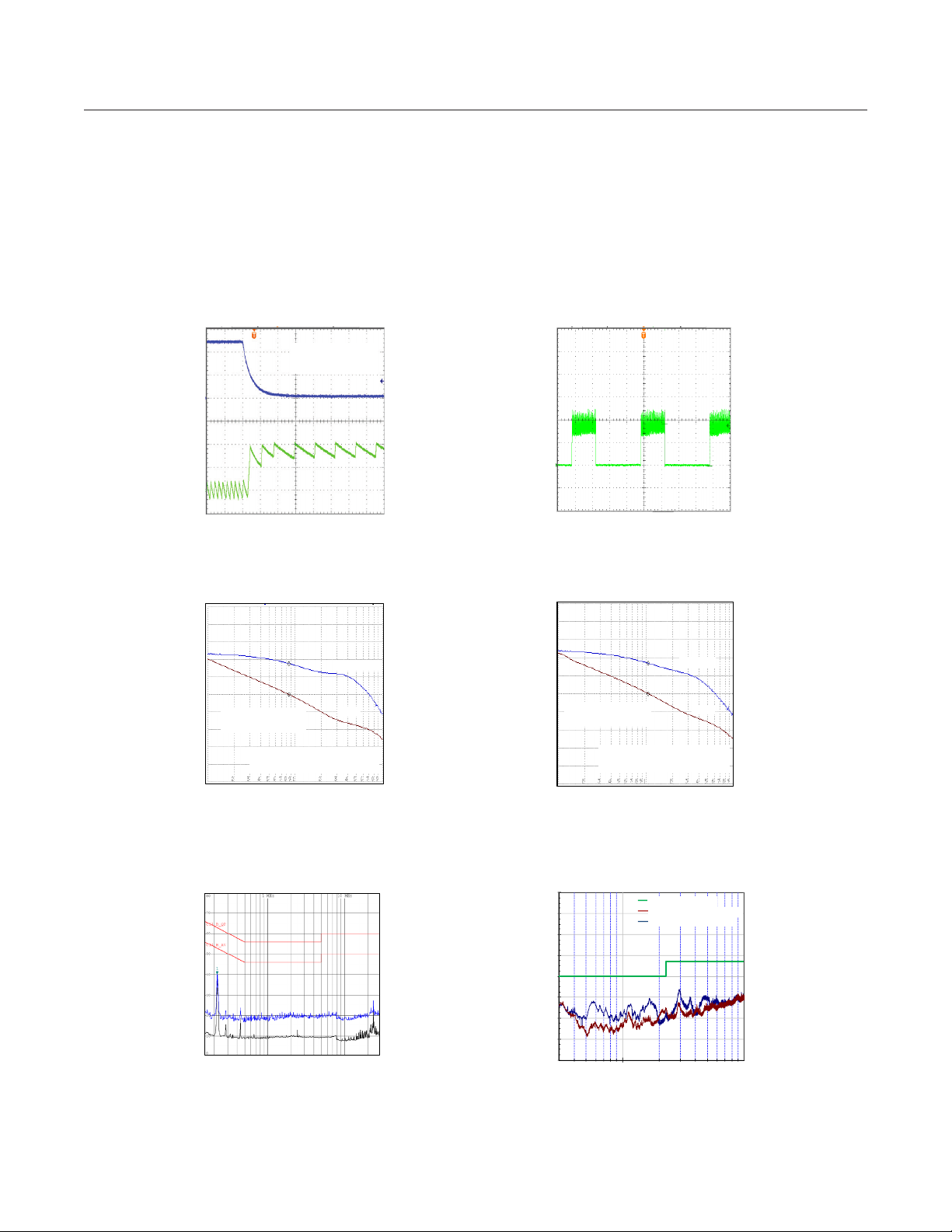
toc50
CONDUCTED EMI CURVE
(5V OUT PUT, 100m A LOAD CURRENT)
0.15
1
10
30
AVERAGE
EMISSIONS
PEAK
EMISSIONS
CONDUCTED EMI (dBµV)
FREQUE NCY (MHz )
10
20
30
40
50
60
70
QUASI-PEAK LIMIT
AVERAGE LIMIT
80
Class B limit
Horizontal limit
Vertical limit
toc51
RADIATED EMI CURVE
(5V OUT PUT, 100m A LOAD CURRENT)
30
100
500
1000
10
20
30
40
50
60
70
0
-10
AMP LITUDE (dBuV/ m)
FREQUE NCY (MHz )
CLASS B LIMIT
HORIZONT AL
VERTICALEMISSION
MAX17552/MAX17552A 60V, 100mA, Ultra-Small, High-Eciency
Synchronous Step-Down DC-DC Converter
with 22µA No-Load Supply Current
Typical Operating Characteristics (continued)
(VIN = 24V, V
GND
= 0V, V
OUT
= 3.3V, V
EN/UVLO
= 1.5V, RT/SYNC = 191kΩ, CIN = 1μF, TA = +25°C unless otherwise noted.)
OVERLOAD PROTECTION
(MAX17552)
V
OUT
I
LX
FIGURE 6
APPLICATION CIRCUIT
= 5V
V
OUT
1ms/div
BODE PLOT
50
40
30
20
10
0
-10
FCR= 8.5KHz,
PHASE MARGIN =
-20
-30
-40
-50
1k 10k 100k
64°
FIGURE 6 APPLICATION CIRCUIT
V
= 5V
OUT
PHA
GAIN
SE
toc46
toc48
5V/div
100mA/div
180
144
108
72
36
0
-36
-72
-108
-144
-180
OVERLOAD PROTECTION
(MAX17552A)
I
LX
20ms/div
BODE PLOT
50
40
30
20
10
0
FCR= 10.5KHz,
-10
PHASE MARGIN = 61°
-20
-30
-40
-50
1k 10k 100k
FIGURE 7 APPLICATION CIRCUIT
= 3.3V
V
OUT
PHASE
GAIN
toc47
toc49
100mA/div
180
144
108
72
36
0
-36
-72
-108
-144
-180
www.maximintegrated.com
Maxim Integrated
│
11
Page 12
MAX17552/MAX17552A 60V, 100mA, Ultra-Small, High-Eciency
Synchronous Step-Down DC-DC Converter
with 22µA No-Load Supply Current
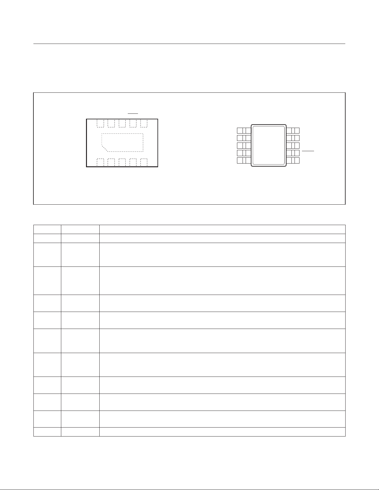
Pin Conguration
TOP VIEW
LX
GND
MODE
10 8 79 6
MAX17552/
MAX17552A
+
1
IN RT/
2
UVLO
3 4
SYNC
TDFN
3mm x 2mm
Pin Description
PIN NAME FUNCTION
1 IN Switching Regulator Input. Connect a X7R 1µF ceramic capacitor from IN to GND for bypassing.
Active-High, Enable/Undervoltage-Detection Input. Pull EN/UVLO to GND to disable the regulator
2 EN/UVLO
3 RT/SYNC
4 SS
5 FB
6 VOUT
output. Connect EN/UVLO to IN for always-on operation. Connect a resistor-divider between IN,
EN/UVLO, and GND to program the input voltage at which the device is enabled and turns on.
Oscillator Timing Resistor Input. Connect a resistor from RT/SYNC to GND to program the switching
frequency from 100kHz to 2.2MHz. See the Switching Frequency (RT/SYNC) section for details. An
external pulse can be applied to RT/SYNC through a coupling capacitor to synchronize the internal clock
to the external pulse frequency. See the External Synchronization section for details.
Soft-Start Capacitor Input. Connect a capacitor from SS to GND to set the soft-start time. Leave SS
unconnected for default 5.1ms internal soft-start.
Output Feedback Connection. Connect FB to a resistor-divider between V
output voltage. See the Adjusting the Output Voltage section for details.
External Bias Input for Internal Control Circuitry. Decouple to GND with a 0.22μF capacitor and connect to
output capacitor positive terminal with a 22.1Ω resistor for applications with an output voltage from 3.3V to
5V. Connect to GND for output voltages < 3.3V and > 5V. See the External Bias section for details.
RESET
SSEN/
V
OUT
+
1 LXIN
EN/UVLO
RT/SYNC
5
FB
2
MAX17552/
3
SS
FB
MAX17552A
4
5
µMAX
10
9
GND
8
MODE
7
RESET
6
V
OUT
3mm x 3mm
and GND to set the
OUT
7 RESET
pulls low if FB voltage drops below 92% of its set value. RESET goes high impedance 2ms after FB
voltage rises above 95% of its set value.
Open-Drain Reset Output. Pull up RESET to an external power supply with an external resistor. RESET
8 MODE
9 GND
10 LX
PFM/PWM Mode-Selection Input. Connect MODE to GND to enable the xed-frequency PWM
operation. Leave MODE unconnected for light-load PFM operation.
Ground. Connect GND to the power ground plane. Connect all the circuit ground connections together at
a single point. See the PCB Layout Guidelines section.
Inductor Connection. Connect LX to the switching side of the inductor. LX is high impedance when the
device is in shutdown.
— EP Exposed Pad (TDFN Only). Connect to the GND pin to the IC.
www.maximintegrated.com
Maxim Integrated
│
12
Page 13
MAX17552/MAX17552A 60V, 100mA, Ultra-Small, High-Eciency
Synchronous Step-Down DC-DC Converter
with 22µA No-Load Supply Current
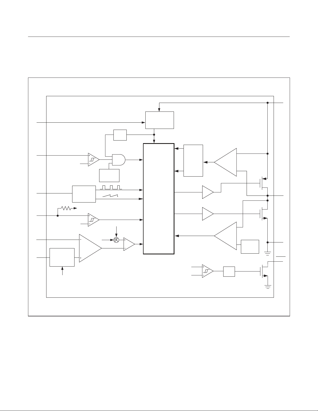
Block Diagram
IN
INTERNAL
V
OUT
EN/UVLO
RT/SYNC
MODE
FB
SS
INTERNAL OR
EXTERNAL
SOFT-START
CONTROL
CLK
1.25V
OSCILLATOR
VCC_INT
1.22V
ERROR
AMPLIFIER
THERMAL
SHUTDOWN
SLOPE
SLOPE
CS
POK
CHIPEN
CLK
MODE SELECT
PWM
MAX17552/MAX17552A
LDO
REGULATOR
VCC_INT
PFM/PWM
CONTROL
LOGIC
PEAK-LIMIT
CURRENT-
PFM
DH
DL
SINK-LIMIT
SENSE
LOGIC
0.76V
HIGH-SIDE
FB
CS
DRIVER
LOW-SIDE
DRIVER
CURRENT-
SENSE
AMPLIFIER
CURRENT
SENSE
AMPLIFIER
2ms
DELAY
NEGATIVE
CURRENT
REF
LX
GND
RESET
www.maximintegrated.com
Maxim Integrated
│
13
Page 14

MAX17552/MAX17552A 60V, 100mA, Ultra-Small, High-Eciency
Synchronous Step-Down DC-DC Converter
with 22µA No-Load Supply Current
Detailed Description
The MAX17552/MAX17552A high-efficiency, high-voltage,
synchronous step-down DC-DC converters with integrated
MOSFETs operate over a 4V to 60V input voltage range.
The converter can deliver output current up to 100mA at
output voltages of 0.8V to 0.9 x VIN. The output voltage
is accurate to within ±1.75% over -40°C to +125°C. The
converter consumes only 22µA of supply current in PFM
mode while regulating the output voltage at no load.
The devices use an internally compensated, peakcurrent-mode control architecture (see the Block
Diagram). On the rising edge of the internal clock, the
high-side pMOSFET turns on. An internal error amplifier
compares the feedback voltage to a fixed internal reference
voltage and generates an error voltage. The error voltage
is compared to a sum of the current-sense voltage and
a slope-compensation voltage by a PWM comparator to
set the “on-time.” During the on-time of the pMOSFET,
the inductor current ramps up. For the remainder of the
switching period (off-time), the pMOSFET is kept off and
the low-side nMOSFET turns on. During the off-time,
the inductor releases the stored energy as the inductor
current ramps down, providing current to the output.
Under overload conditions, cycle-by-cycle current-limit
feature limits inductor peak current by turning off the highside pMOSFET and turning on the low-side nMOSFET.
Mode Selection (MODE)
The devices feature a MODE pin for selecting either
forced-PWM or PFM mode of operation. If the MODE pin
is left unconnected, the devices operate in PFM mode
at light loads. If the MODE pin is grounded, the devices
operate in a constant-frequency forced-PWM mode at all
loads. Mode of operation can be changed on-the-fly during
normal operation of the device.
In PWM mode, the inductor current is allowed to go
negative. PWM operation is useful in frequency-sensitive
applications and provides fixed switching frequency at
all loads. However, the PWM mode of operation gives
lower efficiency at light loads compared to PFM mode of
operation.
PFM mode disables negative inductor current and additionally skips pulses at light loads for high efficiency. In
PFM mode, the inductor current is forced to a fixed peak
of 72mA (typ) (I
rises to 102% (typ) of the nominal voltage. Once the
output reaches 102% (typ) of the nominal voltage, both
high-side and low-side FETs are turned off and the device
) every clock cycle until the output
PFM
enters hibernate operation until the load discharges the
output to 101% (typ) of the nominal voltage. Most of
the internal blocks are turned off in hibernate operation
to save quiescent current. After the output falls below
101% (typ) of the nominal voltage, the devices come
out of hibernate operation, turns on all internal blocks,
and again commences the process of delivering pulses
of energy to the output until it reaches 102% (typ) of the
nominal output voltage. The devices naturally exit PFM
mode when the load current increases to a magnitude of
approximately:
I
- (ΔI/2)
PFM
where ΔI is the peak-peak ripple current in the output
inductor. The part enters PFM mode again if the load
current reduces to approximately (ΔI/2). See the Inductor
Selection section for details. The advantage of the PFM
mode is higher efficiency at light loads because of lower
current drawn from the supply.
Enable Input (EN/UVLO) and Soft-Start (SS)
When EN/UVLO voltage increases above 1.25V (typ), the
devices initiate a soft-start sequence and the duration of
the soft-start depends on the status of the SS pin voltage
at the time of power-up. If the SS pin is not connected,
the devices use a fixed 5ms internal soft-start to ramp
up the internal error-amplifier reference. If a capacitor is
connected from SS to GND, a 5μA current source charges
the capacitor and ramps up the SS pin voltage. The SS
pin voltage is used as reference for the internal error
amplifier. Such a reference ramp up allows the output
voltage to increase monotonically from zero to the final
set value independent of the load current.
EN/UVLO can be used as an input voltage UVLOadjustment input. An external voltage-divider between
IN and EN/UVLO to GND adjusts the input voltage at
which the device turns on or turns off. See the Setting
the Input Undervoltage-Lockout Level section for details.
If input UVLO programming is not desired, connect EN/
UVLO to IN (see the Electrical Characteristics table for
EN/UVLO rising and falling-threshold voltages). Driving
EN/UVLO low disables both power MOSFETs, as well as
other internal circuitry, and reduces IN quiescent current
to below 1.2μA. The SS capacitor is discharged with an
internal pulldown resistor when EN/UVLO is low. If the
EN/UVLO pin is driven from an external signal source,
a series resistance of minimum 1kW is recommended to
be placed between the signal source output and the EN/
UVLO pin, to reduce voltage ringing on the line.
www.maximintegrated.com
Maxim Integrated
│
14
Page 15
42000
MAX17552/MAX17552A 60V, 100mA, Ultra-Small, High-Eciency
Synchronous Step-Down DC-DC Converter
with 22µA No-Load Supply Current
Switching Frequency (RT/SYNC)
Switching frequency of the devices can be programmed
from 100kHz to 2.2MHz by using a resistor connected
from RT/SYNC to GND. The switching frequency (fSW)
is related to the resistor connected at the RT/SYNC pin
(RT) by the following equation, where RT is in kΩ and fSW
is in kHz:
Rf=
T
SW
The switching frequency in ranges of 130kHz to 160kHz
and 230kHz to 280kHz are not allowed for user programming to ensure proper configuration of the internal
adaptive-loop compensation scheme.
External Synchronization
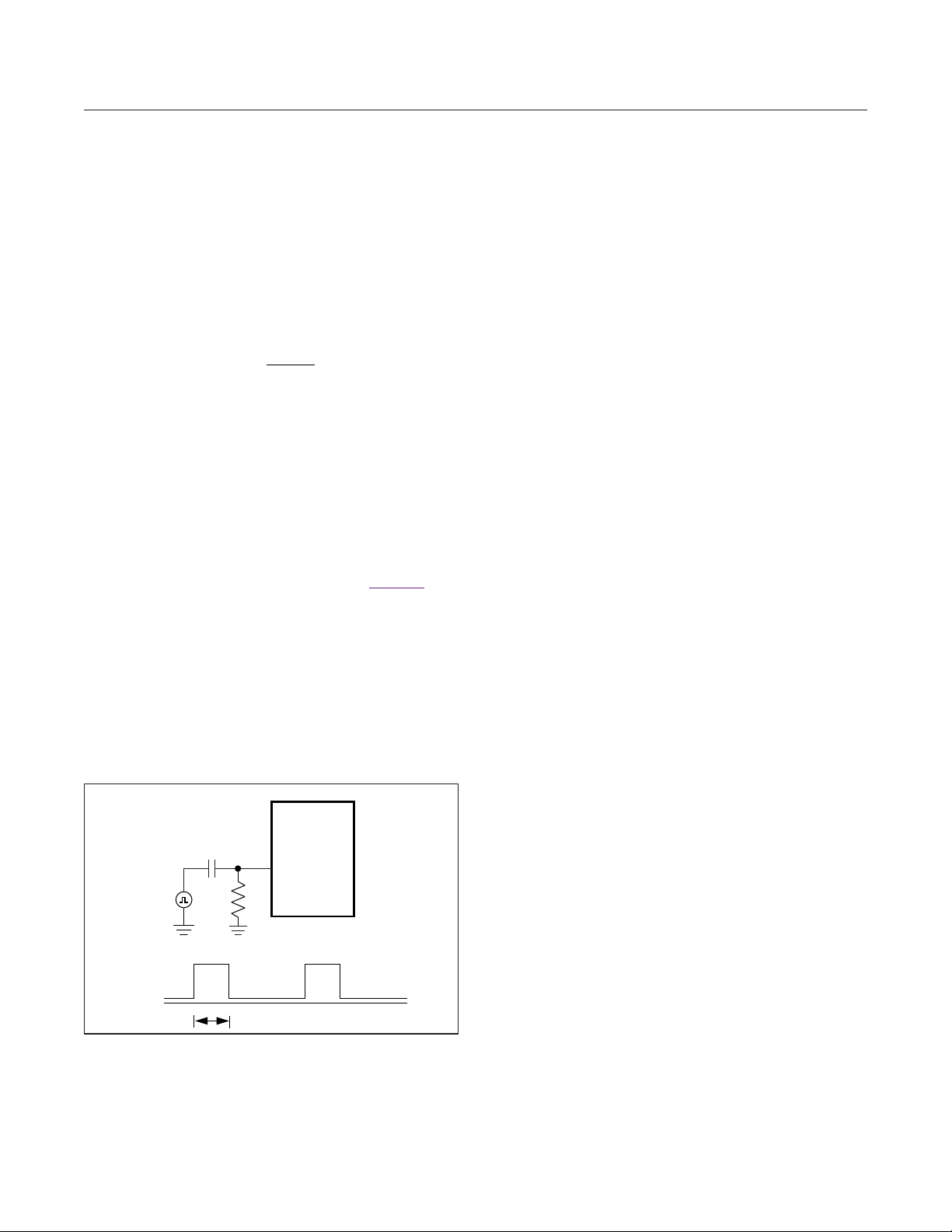
The RT/SYNC pin can be used to synchronize the
device’s internal oscillator to an external system clock.
The external clock should be coupled to the RT/SYNC
pin through a 47pF capacitor, as shown in Figure 1. The
external clock logic high level should be higher than
3V, logic low level lower than 0.5V and the duty cycle
of the external clock should be in the range of 10% to
70%. External clock synchronization is allowed only in
PWM mode of operation (MODE pin connected to GND).
The RT resistor should be selected to set the switching
frequency 10% lower than the external clock frequency.
The external clock should be applied at least 500μs
after enabling the device, for proper configuration of the
internal loop compensation.
MAX17552/
R
T
MAX17552A
RT/SYNC
47pF
CLOCK
SOURCE
V
LOGIC-HIGH
V
LOGIC-LOW
DUTY
Figure 1. Synchronization to an External Clock
External Bias (V
The devices provide a V
blocks from a low-voltage supply. When the V
OUT
)
pin to power the internal
OUT
OUT
pin
voltage exceeds 3.1V, the devices draw switching and
quiescent current from this pin to improve the converter’s
efficiency. In applications with an output voltage setting
from 3.3V to 5V, V
should be decoupled to GND
OUT
with a ceramic capacitor, and should be connected to the
positive terminal of the output capacitor with a resistor
(R4, C1) as shown in the typical application circuits. In
the absence of R4 and C1, the absolute maximum rating of V
(-0.3V) can be exceeded under short-circuit
OUT
conditions, due to oscillations between the ceramic output
capacitor and the inductance of the short-circuit path. In
general, parasitic board or wiring inductance should be
minimized and the output voltage waveform under short
circuit operation should be verified to ensure that the
absolute maximum rating of V
is not exceeded. For
OUT
applications with an output voltage setting less than 3.3V
or greater than 5V, V
should be connected to GND.
OUT
Reset Output (RESET)
The devices include an open-drain RESET output to
monitor output voltage. RESET should be pulled up with
an external resistor to the desired external power supply.
RESET goes high impedance 2ms after the output rises
above 95% of its nominal set value and pulls low when
the output voltage falls below 92% of the set nominal
output voltage.
Startup Into a Prebiased Output
The devices support monotonic startup into a prebiased
output. When the device starts into a prebiased output,
both the high-side and low-side switches are turned off so
that the converter does not sink current from the output.
High-side and low-side switches do not start switching
until the PWM comparator commands the first PWM
pulse, at which point switching commences. The output
voltage is then smoothly ramped up to the target value
in alignment with the internal reference. Such a feature is
useful in applications where digital integrated circuits with
multiple rails are powered.
Operating Input Voltage Range
The maximum operating input voltage is determined
by the minimum controllable on-time, and the minimum
operating input voltage is determined by the maximum
duty cycle and circuit voltage drops. The minimum and
maximum operating input voltages for a given output voltage should be calculated as follows:
www.maximintegrated.com
Maxim Integrated
│
15
Page 16

= +×
tf
SW
10000 x V
MAX17552/MAX17552A 60V, 100mA, Ultra-Small, High-Eciency
Synchronous Step-Down DC-DC Converter
with 22µA No-Load Supply Current
V (I (R 2.6))
+× +
V (I 2.5)
INMIN OUT
where V
the maximum load current, R
the inductor, fSW is the switching frequency (max), D
is the maximum duty cycle (0.9), and t
OUT OUT DCR
D
MAX
V
V
INMAX
is the steady-state output voltage, I
OUT
=
OUT
ONMIN SW
×
is the DC resistance of
DCR
ONMIN
is
OUT
MAX
is the worst-
case minimum controllable switch on-time (128ns)
Overcurrent Protection
The MAX17552 implements a hysteretic cycle-by-cycle
peak-current limit protection scheme to protect the inductor
and internal FETs under output short circuit conditions.
When the inductor peak current exceeds 0.21A (typ), high
side switch is turned off and low side switch is turned
on to discharge the inductor current. Subsequent clock
pulses do not turn on the high-side switch until inductor
current discharges to 0.15A (typ). This operation continues until overload/short circuit is removed on the output.
Since the inductor current is bounded between two limits,
inductor current runaway never happens in this scheme.
Additionally, hysteretic negative peak current limit controls
the low-side switch negative current when it exceeds 0.1A
(typ).
The MAX17552A implements a HICCUP-type overload
protection scheme to protect the inductor and internal
FETs under output short-circuit conditions. When the
inductor peak current exceeds 0.21A (typ) 16 consecutive times, the part enters HICCUP mode. In this mode,
the part is initially operated with hysteretic cycle-by-cycle
peak-current limit that continues for a time period equal
to twice the soft-start time. The part is then turned off
for a fixed 51ms hiccup timeout period. This sequence
of hysteretic inductor current waveforms, followed by a
hiccup timeout period, continues until the short/overload
on the output is removed. Since the inductor current is
bound between two limits, inductor current runway never
happens.
Thermal-Overload Protection
Thermal-overload protection limits the total power dissipation in the IC. When the junction temperature exceeds
+160°C, an on-chip thermal sensor shuts down the
device, turns off the internal power MOSFETs, allowing
the device to cool down. The device turns on after the
junction temperature cools by 20°C.
Applications Information
Inductor Selection
A low-loss inductor having the lowest possible DC resistance
that fits in the allotted dimensions should be selected.
Calculate the required inductance from the equation:
L =
where L is inductance in μH, V
and fSW is the switching frequency in kHz. Calculate the
peak-peak ripple current (ΔI) in the output inductor from
the equation:
1000 V 1
××
OUT
∆=
I
fL
where L is inductance in μH, V
is input voltage and fSW is the switching frequency in kHz.
The saturation current rating of the inductor must exceed
the maximum current-limit value (I
ration current rating should be the maximum of either
0.235A or the value from the equation:
I 0.15
= +
SAT
Vt
where L is inductance in H, V
voltage and t
ON-MIN
is worst case minimum on time
(128ns).
Once the L value is known, the next step is to select the
right core material. Ferrite and powdered iron are commonly available core materials. Ferrite cores have low
core losses and are preferred for high-efficiency designs.
Powdered iron cores have more core losses and are relatively cheaper than ferrite cores.
Input Capacitor Selection
Small ceramic input capacitors are recommended for the
IC. The input capacitor reduces peak current drawn from
the power source and reduces noise and voltage ripple
on the input caused by the switching circuitry. A minimum
of 1μF, X7R-grade capacitor in a package larger than 0805
is recommended for the input capacitor of the IC to keep the
input-voltage ripple under 2% of the minimum input voltage,
and to meet the maximum ripple-current requirements.
OUT
f
is output voltage
OUT
V
OUT
−
V
IN
×
SW
is output voltage, VIN
OUT
PEAK-LIMIT
INMAX ON MIN
×
−
L
is maximum input
INMAX
). The satu-
www.maximintegrated.com
Maxim Integrated
│
16
Page 17
tSS> 0.05 x C
x V
SS SS
MAX17552/MAX17552A 60V, 100mA, Ultra-Small, High-Eciency
Synchronous Step-Down DC-DC Converter
with 22µA No-Load Supply Current
Output Capacitor Selection
Small ceramic X7R-grade output capacitors are recommended for the devices. The output capacitor has two
functions. It stores sufficient energy to support the output
voltage under load transient conditions and stabilizes the
device’s internal control loop. Usually the output capacitor
is sized to support a step load of 50% of the maximum
output current in the application, such that the outputvoltage deviation is less than 3%. Calculate the minimum
required output capacitance from the following equations:
Frequency
Range
(kHz)
100 to 130
160 to 230
280 to 2200
Minimum Output
Capacitance
(μF)
50
V
OUT
25
V
OUT
17
V
OUT
It should be noted that dielectric materials used in ceramic
capacitors exhibit capacitance loss due to DC bias levels and
should be appropriately derated to ensure the required
output capacitance is obtained in the application.
Soft-Start Capacitor Selection
The devices offer a 5.1ms internal soft-start when the
SS pin is left unconnected. When adjustable soft-start
time is required, connect a capacitor from SS to GND
to program the soft-start time. The minimum soft-start time
is related to the output capacitance (C
voltage(V
) by the following equation.
OUT
OUT
where tSS is in milliseconds and C
) and the output
OUT
OUT
is in µF.
OUT
Soft-start time (tSS) is related to the capacitor connected at
SS (CSS) by the following equation:
C 6.25 t= ×
where tSS is in milliseconds and CSS is in nanofarads.
Setting the Input Undervoltage-Lockout Level
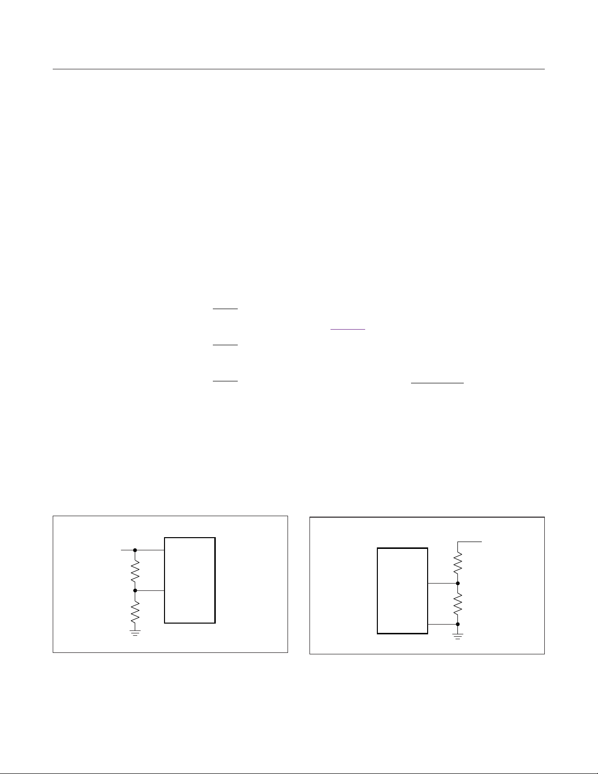
The devices offer an adjustable input undervoltagelockout level. Set the voltage at which the device turns on
with a resistive voltage-divider connected from IN to GND
(see Figure 2). Connect the center node of the divider to
EN/UVLO.
Choose R1 to be 3.3MΩ max and then calculate R2 as
follows:
×
R1 1.25
=
R2
(V - 1.25)
INU
where V
to turn on.
If the EN/UVLO pin is driven from an external signal
source, a series resistance of minimum 1kΩ is recommended to be placed between the signal source output
and the EN/UVLO pin to reduce voltage ringing on the
line.
is the voltage at which the device is required
INU
Figure 2. Adjustable EN/UVLO Network
www.maximintegrated.com
V
V
IN
IN
R1
R2
MAX17552/
MAX17552A
EN/UVLO
Figure 3. Setting the Output Voltage
MAX17552/
MAX17552A
FB
GND
OUT
R1
R2
Maxim Integrated
│
17
Page 18
=××
P VI
( )
MAX17552/MAX17552A 60V, 100mA, Ultra-Small, High-Eciency
Synchronous Step-Down DC-DC Converter
with 22µA No-Load Supply Current
4.7Ω
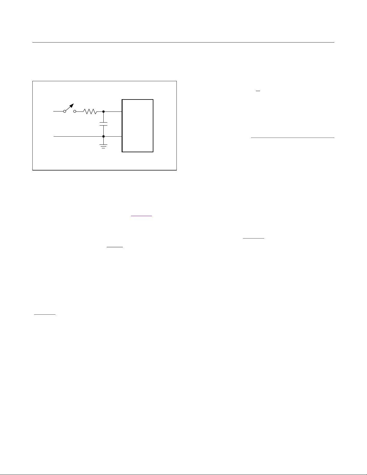
Figure 4. Transient Protection
IN
IN
µF
MAX17552/
MAX17552A
GND
C
1
Adjusting the Output Voltage
The output voltage can be programmed from 0.8V to 0.9V
x VIN. Set the output voltage by connecting a resistordivider from output to FB to GND (see Figure 3). Choose
R2 in the range of 25kΩ to 100kΩ and calculate R1 with
the following equation:
V
OUT
= ×
R1 R 2 1
0.8
−
Transient Protection
In applications where fast line transients or oscillations
with a slew rate in excess of 15V/µs are expected during power-up or steady-state operation, the MAX17552/
MAX17552A should be protected with a series resistor
that forms a lowpass filter with the input ceramic capacitor
(Figure 4). These transients can occur in conditions such
as hot-plugging from a low-impedance source or due to
inductive load switching and surges on the supply lines.
Power Dissipation
At a particular operating condition, the power losses that
lead to temperature rise of the device are estimated as
follows:
P P -1 - (I R )
LOSS OUT OUT DCR
where P
OUT
OUT OUT OUT
is the output power, η is the efficiency of
power conversion, and R
1
η
= ×
is the DC resistance of the
DCR
2
output inductor. See the Typical Operating Characteristics
for the power-conversion efficiency or measure the efficiency to determine the total power dissipation.
The junction temperature (TJ) of the device can be
estimated at any ambient temperature (TA) from the
following equation:
TT P= +θ ×
J A JA LOSS
where θJA is the junction-to-ambient thermal impedance
of the package.
Junction temperature greater than +125°C degrades
operating lifetimes.
PCB Layout Guidelines
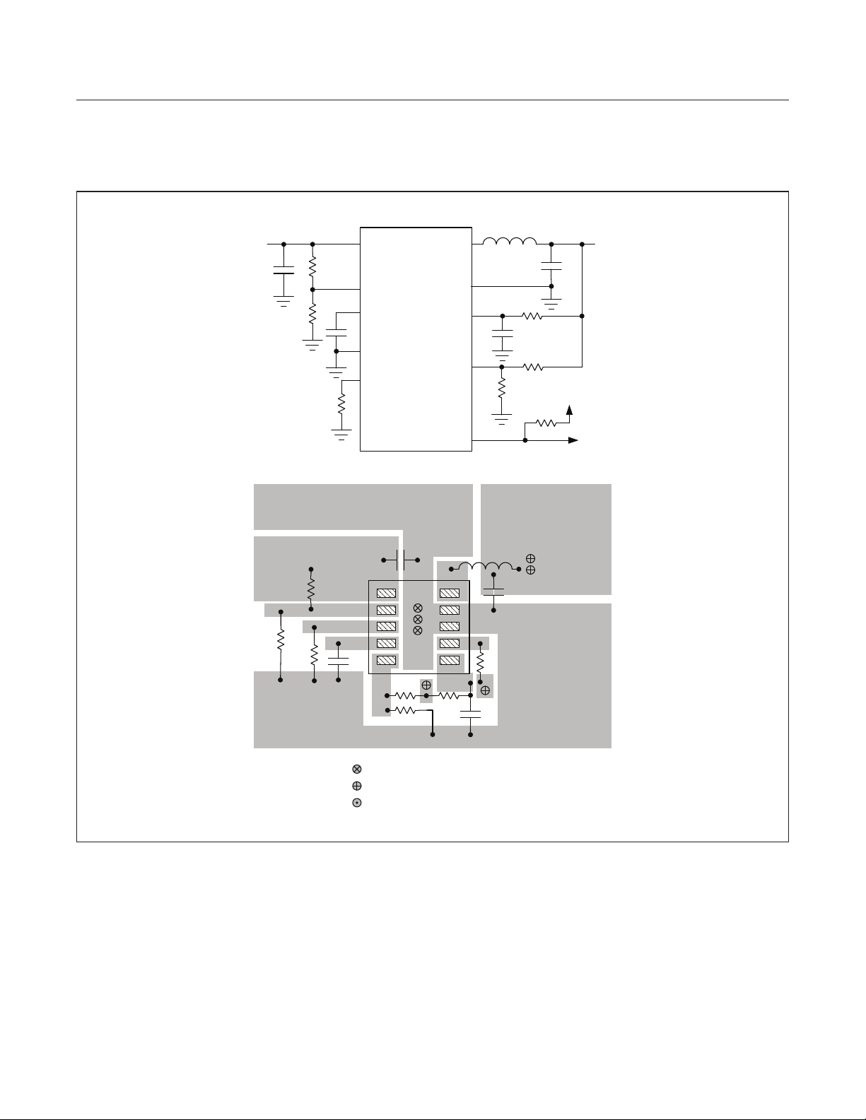
Careful PCB layout (Figure 5) is critical to achieve clean
and stable operation. The switching power stage requires
particular attention. Follow these guidelines for good PCB
layout:
● Place the input ceramic capacitor as close as possible
to VIN and GND pins
● Minimize the area formed by the LX pin and inductor
connection to reduce the radiated EMI
● Ensure that all feedback connections are short and
direct
● Route high-speed switching node (LX) away from the
signal pins
For a sample PCB layout that ensures the first-pass
success, refer to the MAX17552/MAX17552A evaluation
kit data sheet.
www.maximintegrated.com
Maxim Integrated
│
18
Page 19
MAX17552/MAX17552A 60V, 100mA, Ultra-Small, High-Eciency
Synchronous Step-Down DC-DC Converter
with 22µA No-Load Supply Current
V
IN
C
IN
GND PLANE
PLANE
V
IN
R2
LX
GND
MODE
C
F
R5
L1
RESET
R6
C
F
L1
C
OUT
C
OUT
IN
EN/UVLO
SS
MODE
RT/SYNC
IN
SS
FB
MAX17552/
MAX17552A
C
IN
U1
R4
R5
R1
R2
R1
R3
R3
EN/UVLO
RT/SYNC
C
SS
C
SS
LX
GND
VOUT
FB
RESET
VOUT
R7
R7
R4
R6
V
OUT
GND PLANE
V
V
OUT
PLANE
OUT
Figure 5. Layout Guidelines
www.maximintegrated.com
Vias to Bottom-Side Ground Plane
Vias to V
OUT
Vias to RESET
Maxim Integrated
│
19
Page 20
MAX17552/MAX17552A 60V, 100mA, Ultra-Small, High-Eciency
Synchronous Step-Down DC-DC Converter
with 22µA No-Load Supply Current
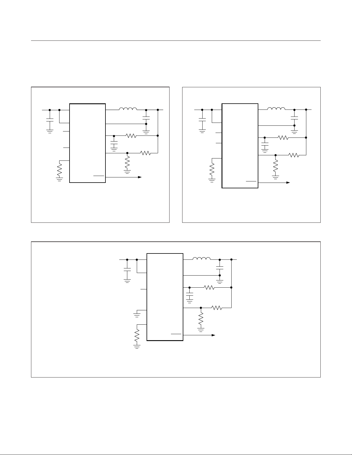
Typical Application Circuits
C1
0.22
220
L1
22.1
µ
F
V
IN
6V TO 60V
C
IN
1µF
R3
191k
Ω
SWITCHING FREQUENCY = 220kHz
L1 COILCRAFT LPS5030-224M
MURATA 10µF/X7R/6.3V/1206 (GRM31CR70J106K)
C
OUT
C
MURATA 1µF/X7R/100V/1206 (GRM31CR72A105K)
IN
MAX17552/
IN
MAX17552A
EN/UVLO
SS
MODE
RT/SYNC
GND
V
OUT
RESET
LX
FB
Figure 6. High-Efficiency 5V, 100mA Regulator
V
IN
6V TO 60V
C
IN
1µF
69.8k
µ
R4
R3
H
R2
49.9k
Ω
C
10µF
Ω
OUT
Ω
261k
5V, 100mA
R1
Ω
IN
EN/UVLO
SS
MODE
RT/SYNC
V
OUT
MAX17552/
MAX17552A
V
IN
4V TO 60V
C
IN
1µF
R3
191k
Ω
SWITCHING FREQUENCY = 220kHz
L1 COILCRAFT LPS5030-154M
MURATA 10µF/X7R/6.3V/1206 (GRM31CR70J106K)
C
OUT
C
MURATA 1µF/X7R/100V/1206 (GRM31CR72A105K)
IN
IN
MAX17552/
MAX17552A
EN/UVLO
SS
MODE
RT/SYNC
GND
V
OUT
RESET
LX
FB
Figure 7. High-Efficiency 3.3V, 100mA Regulator
GND
V
OUT
RESET
L1
µ
H
C1
0.22
100
C
OUT
10µF
R4
22.1
µ
F
R2
49.9k
LX
FB
Ω
261k
Ω
R1
5V, 100mA
Ω
V
OUT
C1
0.22
150
L1
µ
H
C
OUT
10µF
R4
Ω
22.1
µ
F
R2
49.9k
158k
Ω
3.3V, 100mA
R1
Ω
V
OUT
SWITCHING FREQUENCY = 600kHz
L1 COILCRAFT LPS3015-104M
C
OUT
C
IN
Figure 8. Small Footprint 5V, 100mA Regulator
www.maximintegrated.com
MURATA 10µF/X7R/6.3V/0805 (GRM21BR70J106K)
MURATA 1µF/X7R/100V/1206 (GRM31CR72A105K)
Maxim Integrated
│
20
Page 21
MAX17552/MAX17552A 60V, 100mA, Ultra-Small, High-Eciency
Synchronous Step-Down DC-DC Converter
with 22µA No-Load Supply Current
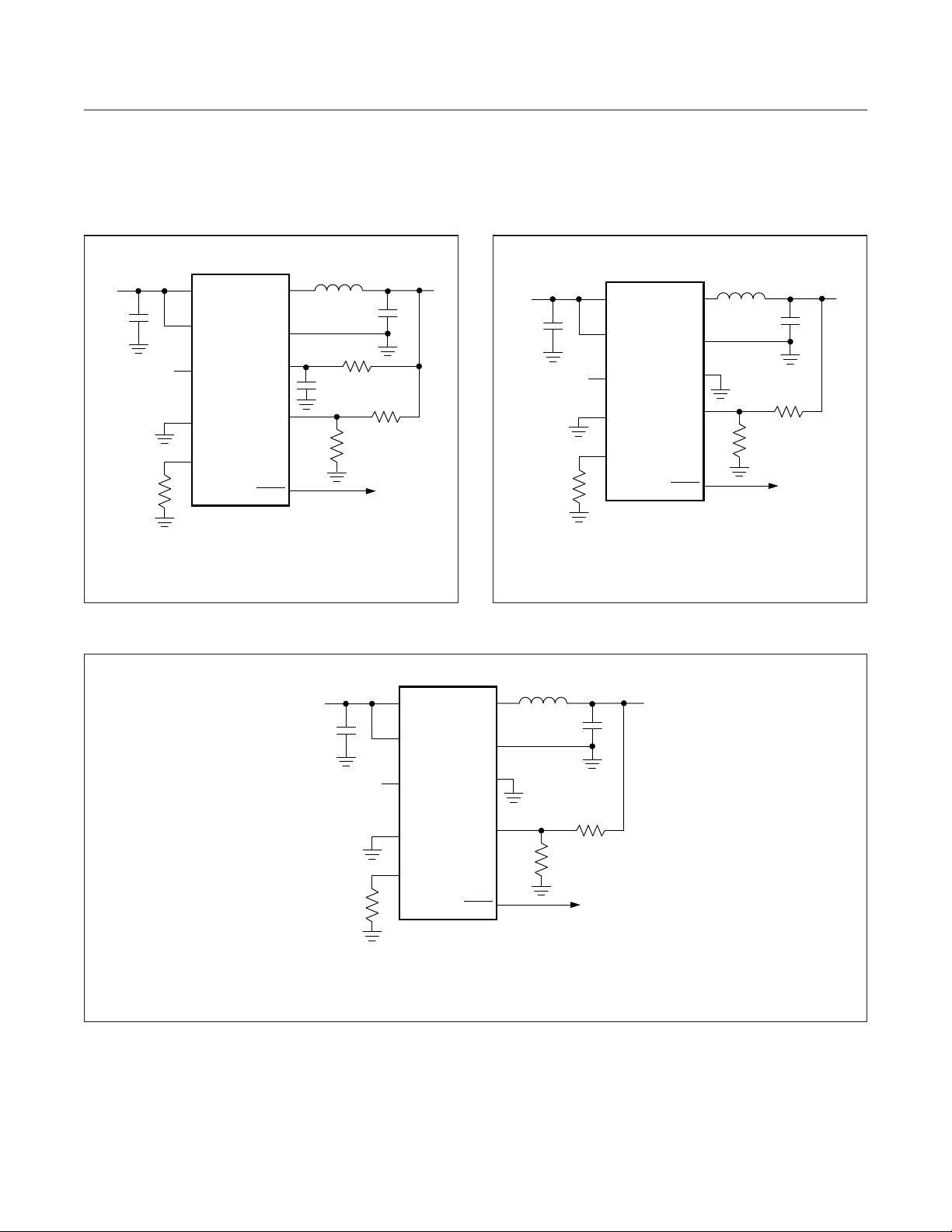
Typical Application Circuits (continued)
V
IN
4V TO 45V
C
IN
1µF
R3
69.8k
Ω
SWITCHING FREQUENCY = 600kHz
L1 COILCRAFT LPS3015-683M
MURATA 10µF/X7R/6.3V/0805 (GRM21BR70J106K)
C
OUT
C
MURATA 1µF/X7R/100V/1206 (GRM31CR72A105K)
IN
IN
MAX17552/
MAX17552A
EN/UVLO
SS
MODE
RT/SYNC
GND
V
OUT
RESET
LX
FB
L1
68
C1
µ
0.22
V
IN
15V TO 60V
C
IN
1µF
V
158k
R1
OUT
3.3V, 100mA
Ω
µ
H
C
OUT
10µF
R4
Ω
22.1
F
R2
49.9k
Ω
V
IN
4V TO 24V
C
IN
1µF
R3
69.8k
Ω
SWITCHING FREQUENCY = 600kHz
L1 COILCRAFT LPS3015-333M
MURATA 10µF/X7R/6.3V/1206 (GRM31CR70J106K)
C
OUT
C
MURATA 1µF/X7R/100V/1206 (GRM31CR72A105K)
IN
IN
MAX17552/
MAX17552A
EN/UVLO
SS
MODE
RT/SYNC
GND
V
OUT
RESET
LX
FB
L1
µ
H
33
C
OUT
10µF
R2
100k
127k
Ω
1.8V, 100mA
R1
Ω
V
OUT
Figure 10. Small Footprint 1.8V, 100mA RegulatorFigure 9. Small Footprint 3.3V, 100mA Regulator
IN
MAX17552/
MAX17552A
EN/UVLO
GND
L1
µ
H
220
LX
C
10µF
OUT
V
OUT
12V, 100mA
SS
MODE
RT/SYNC
R3
69.8k
Ω
SWITCHING FREQUENCY = 600kHz
L1 COILCRAFT LPS5030-224M
MURATA 10µF/X7R/16V/1206 (GRM31CR71C106K)
C
OUT
C
MURATA 1µF/X7R/100V/1206 (GRM31CR72A105K)
IN
Figure 11. Small Footprint 12V, 100mA Step-Down Regulator
www.maximintegrated.com
V
OUT
RESET
R1
Ω
R2
24.9k
Ω
348k
Maxim Integrated
│
21
FB
Page 22

MAX17552/MAX17552A 60V, 100mA, Ultra-Small, High-Eciency
Synchronous Step-Down DC-DC Converter
with 22µA No-Load Supply Current
Ordering Information
PART TEMP RANGE PIN-PACKAGE
MAX17552ATB+ -40°C to +125°C 10 TDFN-EP*
MAX17552AUB+ -40°C to +125°C 10 μMAX
MAX17552AATB+ -40°C to +125°C 10 TDFN-EP*
MAX17552AAUB+ -40°C to +125°C 10 μMAX
+Denotes a lead(Pb)-free/RoHS-compliant package.
*EP = Exposed pad.
Chip Information
PROCESS: BiCMOS
www.maximintegrated.com
Maxim Integrated
│
22
Page 23
MAX17552/MAX17552A 60V, 100mA, Ultra-Small, High-Eciency
Synchronous Step-Down DC-DC Converter
with 22µA No-Load Supply Current
Revision History
REVISION
NUMBER
0 2/14 Initial release —
1 6/14 Added statement regarding EN/UVLO connection 11
2 2/15 Updating to include MAX17552A 1-20
3 6/15
4 9/17
5 8/18 Updated the Mode Selection (MODE) section. 14
REVISION
DATE
DESCRIPTION
Included small solution-size TOCs in Typical Operating Characteristics section
and updated Typical Application Circuit diagrams
Updated Features and Benets, Mode Selection (MODE), Setting the Input
Undervoltage-Lockout Level, and Power Dissipation sections. Updated the
Electrical Characteristics table global characteristics. Inserted new Note 1 and
updated Absolute Maximum Ratings, and added TOC50 and TOC51.
PAGES
CHANGED
2, 6–10,
19, 20
1, 3–5,
11, 14,
17–18
For pricing, delivery, and ordering information, please visit Maxim Integrated’s online storefront at https://www.maximintegrated.com/en/storefront/storefront.html.
Maxim Integrated cannot assume responsibility for use of any circuitry other than circuitry entirely embodied in a Maxim Integrated product. No circuit patent licenses
are implied. Maxim Integrated reserves the right to change the circuitry and specications without notice at any time. The parametric values (min and max limits)
shown in the Electrical Characteristics table are guaranteed. Other parametric values quoted in this data sheet are provided for guidance.
Maxim Integrated and the Maxim Integrated logo are trademarks of Maxim Integrated Products, Inc.
©
2018 Maxim Integrated Products, Inc.
│
23
 Loading...