

Page 1
For pricing, delivery, and ordering information, please contact Maxim Direct at 1-888-629-4642,
or visit Maxim’s website at www.maxim-ic.com.
MAX17020
Dual Quick-PWM Step-Down Controller
with Low-Power LDO, RTC Regulator
________________________________________________________________
Maxim Integrated Products
1
Ordering Information
19-4118; Rev 2; 2/09
o
o
o
o
o
o
o
o
o
o
o
o
o
o
o
General Description
The MAX17020 is a dual Quick-PWM™ step-down
power-supply (SMPS) controller with synchronous rectification, intended for main 5V/3.3V or I/O 1.5V/1.05V
power generation in battery-powered systems. Lowside MOSFET sensing provides a simple low-cost,
highly efficient current sense for valley current-limit
protection. Combined with the output overvoltage and
undervoltage protection features, this current limit
ensures robust output supplies.
The 5V/3.3V or 1.5V/1.05V SMPS outputs can save
power by operating in pulse-skipping mode or in ultrasonic mode to avoid audible noise. Ultrasonic mode
forces the controller to maintain switching frequencies
greater than 20kHz at light loads.
An internal 100mA linear regulator can be used to
either generate the 5V bias needed for power-up or
other lower power “always-on” suspend supplies. An
independent bypass input allows automatic bypassing
of the linear regulator when the SMPS is active.
This main controller also includes a secondary feedback input that triggers an ultrasonic pulse (DL1 turned
on) if the SECFB voltage drops below its threshold voltage. This refreshes an external charge pump driven by
DL1 without overcharging the output voltage.
The device includes independent shutdown controls to
simplify power-up and power-down sequencing. To
prevent current surges at startup, the internal voltage
target is slowly ramped up from zero to the final target
over a 1ms period. To prevent the output from ringing
below ground in shutdown, the internal voltage target
is ramped down from its previous value to zero over a
1ms period. Two independent power-good outputs
simplify the interface with external controllers.
The MAX17020 is a pin-for-pin replacement of the
MAX8778.
Features
Applications
+
Denotes a lead(Pb)-free/RoHS-compliant package.
*
EP = Exposed pad.
Dual Quick-PWM
Internal 100mA 5V or Adjustable Linear Regulator
Independent LDO Bypass Input
Internal Boost Diodes
Secondary Feedback Input Maintains Charge Pump
3.3V 5mA RTC Power (Always On)
OUT1: 5V or 1.5V Fixed or 0.7V Adjustable
Feedback
OUT2: 3.3V or 1.05V Fixed or Dynamic Adjustable
Dynamic 0V to 2V REFIN2 Input on Second SMPS
2V ±1% 50µA Reference
6V to 24V Input Range (28V max)
Ultrasonic Mode
Independent SMPS and LDO Enable Controls
Independent SMPS Power-Good Outputs
Minimal Component Count
Notebook Computers
Main System Supply (5V and 3.3V Supplies)
I/O System Supply (1.5V and 1.05V Supplies)
Graphic Cards
DDR1, DDR2, DDR3 Power Supplies
Game Consoles
Low-Power I/O and Chipset Supplies
Two-to-Four Li+ Cell Battery-Powered Devices
PDAs and Mobile Communicators
Telecommunication
MAX17020
THIN QFN (T3255-4)
5mm x 5mm
TOP VIEW
A "+" SIGN FIRST-PIN INDICATOR DENOTES A LEAD-FREE PACKAGE.
29
30
28
27
12
11
13
TON
ONLDO
RTC
IN
LDO
14
REF
DL2
AGND
SECFB
BST2
V
DD
DL1
12
PGOOD2
4567
2324 22 20 19 18
SKIP
OUT2
ON1
PGOOD1
ILIM1
FB1
V
CC
PGND
3
21
31
10
ILIM2
OUT1
32
9
REFIN2
+
BYP
ON2
26
15
DH1
DH2
25
16
LX1
LDOREFIN
BST1
8
17
LX2
Pin Configuration
Quick-PWM is a trademark of Maxim Integrated Products, Inc.
EVALUATION KIT
AVAILABLE
PART TEMP RANGE PIN-PACKAGE
M AX 17020E TJ+ -40°C to +85°C 32 TQFN
Page 2
MAX17020
Dual Quick-PWM Step-Down Controller
with Low-Power LDO, RTC Regulator
2 _______________________________________________________________________________________
ABSOLUTE MAXIMUM RATINGS
ELECTRICAL CHARACTERISTICS
(Circuit of Figure 1, no load on LDO, RTC, OUT1, OUT2, and REF, VIN= 12V, VDD= VCC= V
SECFB
= 5V, V
REFIN2
= 1.0V, BYP =
LDOREFIN = GND, ONLDO = IN, ON1 = ON2 = V
CC
, TA= 0°C to +85°C, unless otherwise noted. Typical values are at TA= +25°C.)
(Note 3)
Stresses beyond those listed under “Absolute Maximum Ratings” may cause permanent damage to the device. These are stress ratings only, and functional
operation of the device at these or any other conditions beyond those indicated in the operational sections of the specifications is not implied. Exposure to
absolute maximum rating conditions for extended periods may affect device reliability.
IN, ONLDO to GND ................................................-0.3V to +28V
V
DD
, VCCto GND .....................................................-0.3V to +6V
RTC, LDO to GND ....................................................-0.3V to +6V
OUT_ to GND ...........................................................-0.3V to +6V
ON1, ON2 to GND....................................................-0.3V to +6V
PGOOD_ to GND........................................-0.3V to (V
CC
+ 0.3V)
REF, ILIM_, TON, SKIP to GND..................-0.3V to (V
CC
+ 0.3V)
FB1, REFIN2, LDOREFIN to GND ............................-0.3V to +6V
SECFB to GND .........................................................-0.3V to +6V
BYP to GND..............................................-0.3V to (V
LDO
+ 0.3V)
GND to PGND .......................................................-0.3V to +0.3V
DL_ to PGND..............................................-0.3V to (V
DD
+ 0.3V)
BST_ to GND ..........................................................-0.3V to +34V
BST_ to V
DD
............................................................-0.3V to +28V
DH1 to LX1 ..............................................-0.3V to (V
BST1
+ 0.3V)
BST1 to LX1..............................................................-0.3V to +6V
DH2 to LX2 ..............................................-0.3V to (V
BST2
+ 0.3V)
BST2 to LX2..............................................................-0.3V to +6V
LDO, RTC, REF Short Circuit to GND.........................Momentary
RTC Current Continuous.....................................................+5mA
LDO Current (Internal Regulator)
Continuous..................................................................+100mA
LDO Current (Switched Over) Continuous .....................+200mA
Continuous Power Dissipation (T
A
= +70°C)
32-Pin 5mm x 5mm TQFN
(derate 34.5mW/°C above +70°C).................................2.76W
Operating Temperature Range ...........................-40°C to +85°C
Junction Temperature......................................................+150°C
Storage Temperature Range .............................-65°C to +150°C
Lead Temperature (soldering, 10s) .................................+300°C
Dual Mode is a trademark of Maxim Integrated Products, Inc.
PARAMETER SYMBOL CONDITIONS MIN TYP MAX UNITS
INPUT SUPPLIES
IN Standby Supply Current I
IN Shutdown Supply Current I
IN Supply Current I
VCC Supply C urrent I
PWM CONTROLLERS
OUT1 Output Voltage Accuracy
(Note 1)
OUT1 Voltage Adjust Range 0.7 5.5 V
FB1 Dual-Mode™ Threshold
Voltage Leve ls
FB1 Input B ia s Current I
IN(STBY)
IN(SHDN)
IN
CC
V
OUT1
V
FB1
FB1
VIN = 6V to 24V, ON1 = ON2 = GND,
ONLDO = V
VIN = 4.5V to 24V,
ON1 = ON2 = ONLDO = GND
ON1 = ON2 = REFIN2 = VCC,
SKIP = FB1 = GND,
V
OUT2
ON1 = ON2 = REFIN2 = VCC,
SKIP = FB1 = GND,
V
OUT2
5V preset output: FB1 = GND,
= 12V, SKIP = V
V
IN
1.5V preset output: FB1 = VCC (5V),
= 12V, SKIP = V
V
IN
Adju stable feedback output,
= 12V, SKIP = V
V
IN
Low 0.04 0.110
High
V
FB1
CC
= 3.5V, V
= 3.5V, V
= 0.8V, TA = +25°C -0.2 +0.2 µA
OUT1
OUT1
= 5.3V
= 5.3V
CC
CC
CC
85 175 µA
50 70 µA
0.1 0.2 mA
1.0 1.5 mA
4.95 5.00 5.05
1.485 1.50 1.515
0.693 0.700 0.707
V
-
CC
1.6V
VCC -
0.7V
V
V
Page 3
MAX17020
Dual Quick-PWM Step-Down Controller
with Low-Power LDO, RTC Regulator
_______________________________________________________________________________________ 3
ELECTRICAL CHARACTERISTICS (continued)
(Circuit of Figure 1, no load on LDO, RTC, OUT1, OUT2, and REF, VIN= 12V, VDD= VCC= V
SECFB
= 5V, V
REFIN2
= 1.0V, BYP =
LDOREFIN = GND, ONLDO = IN, ON1 = ON2 = V
CC
, TA= 0°C to +85°C, unless otherwise noted. Typical values are at TA= +25°C.)
(Note 3)
PARAMETER SYMBOL CONDITIONS MIN TYP MAX UNITS
3.3V preset output: REFIN2 = VCC (5V),
V
= 12V, SKIP = V
OUT2 Output Voltage Accuracy
(Note 1)
V
OUT2
IN
1.05V preset output: REFIN2 = RTC (3.3V),
V
= 12V, SKIP = V
IN
Tracking output: V
= 12V, SKIP = V
V
IN
CC
CC
REFIN2
CC
= 1.0V,
OUT2 Voltage-Adjust Range 0 2 V
REFIN2 Voltage-Adjust Range 0 2 V
V
= 2.2V, TA = +25°C -0.1 +0.1
REFIN2 Input Bias Current I
REFIN2 Dual-Mode Threshold
Voltage Leve ls
Load Regulation Error
REFIN2
REFIN2
V
= 0, TA = +25°C -0.5 +0.1
REFIN2
Low (REFIN2 = RTC) 2.2 3.0
High (REFIN2 = V
Either SMPS, SKIP = VCC, I
Either SMPS, SKIP = REF, I
Either SMPS, SKIP = GND, I
CC
)
= 0 to 5A -0.1
LOAD
= 0 to 5A -1.7
LOAD
= 0 to 5A -1.5
LOAD
Line Regulation Error Either SMPS, VIN = 6V to 24V 0.005 %/V
TON = GND or REF
(400kHz)
TON = V
(200kHz) 1895 2105 2315
CC
TON = GND (500kH z) 475 555 635
TON = REF or V
CC
(300kHz)
DH1 On-Time t
DH2 On-Time t
Minimum Off-Time t
OFF(MIN)
Soft-Start/Stop Slew Rate t
Soft-Start/Stop Slew Rate t
Dynamic REFIN2 Slew Rate t
Ultrasonic Operating Frequency f
SW(USONIC)
SECFB Threshold Voltage V
SECFB Input Bias Current I
VIN = 12V,
ON1
V
OUT1
(Note 2)
VIN = 12V,
V
ON2
OUT2
(Note 2)
(Note 2) 250 400 ns
SS
SS
DYN
Risi ng/falling edge on ON1 or ON2 (preset)
Risi ng/falling edge on ON2 (REFIN2 AD J)
Risi ng edge on REFIN2 8 mV/µs
SKIP = open (REF) 20 27 kHz
SECFB
SECFB VSECFB
1.94 2.0 2.06 V
= 5.0V
= 3.3V
= 2.2V, TA = +25°C -0.2 +0.2 µA
LINEAR REGULATOR (LDO)
VIN = 24V, LDOREFIN = BYP = GND,
< 100mA
LDO
< 100mA
LDO
= 0.5V,
LDO
= 2 x V
< 100mA
LDOR EFI N
LDOR EFI N
0.3 2.0 V
= 0 or 2V, TA = +25°C -0.5 +0.5 µA
LDO Output-Voltage Accuracy V
LDOREFIN Input Range V
LDOREFIN Leakage Current I
LDOREFIN VLDO
LDOR EFI N VLDOREFIN
LDOREFIN Dual-Mode
Threshold Voltage
LDO
0mA < I
VIN = 24V, LDOREFIN = VCC, BYP = GND,
0mA < I
VIN = 24V, BYP = GND, V
0mA < I
LDOREFIN low threshold 0.1 0.15 0.20
LDOREFIN high threshold
3.267 3.30 3.333
1.040 1.050 1.060
V
0.995 1.00 1.005
µA
V
CC
1.0V
-
V
CC
0.4V
V
-
%
895 1052 1209
833 925 1017
1
ms
ns
ns
1 mV/µs
4.90 5.0 5.10
3.23 3.3 3.37
V
0.960 1.0 1.040
V
-
CC
2V
VCC -
1.5V
VCC -
0.9V
V
Page 4
MAX17020
Dual Quick-PWM Step-Down Controller
with Low-Power LDO, RTC Regulator
4 _______________________________________________________________________________________
ELECTRICAL CHARACTERISTICS (continued)
(Circuit of Figure 1, no load on LDO, RTC, OUT1, OUT2, and REF, VIN= 12V, VDD= VCC= V
SECFB
= 5V, V
REFIN2
= 1.0V, BYP =
LDOREFIN = GND, ONLDO = IN, ON1 = ON2 = V
CC
, TA= 0°C to +85°C, unless otherwise noted. Typical values are at TA= +25°C.)
(Note 3)
)
)
PARAMETER SYMBOL CONDITIONS MIN TYP MAX UNITS
LDO Short-Circuit Current I
LDO Regulation Reduction/
Bypass Switchover Threshold
LDO Bypass Switchover
Threshold
LDO Bypass Switchover
Startup Timeout
LDO Bypass Switch Resistance LDO to BYP, V
VCC Undervoltage-Lockout
(UVLO) Threshold
Thermal-Shutdown Threshold T
3.3V ALWAYS-ON LINEAR REGULATOR (RTC)
RTC Output-Voltage Accuracy V
RTC Short-Circuit Current I
REFERENCE (REF)
Reference Voltage V
Reference Load-Regulation Error ΔV
REF Lockout Voltage V
OUT1 FAULT DETECTION
OUT1 Overvoltage Trip
Threshold
OU T1 Over voltag e Faul tP r op ag ati on D el ay
OUT1 Undervoltage-Protection
Trip Threshold
OUT1 Output-Undervoltage
Fault-Propagation Delay
PGOOD1 Lower Trip Threshold
PGOOD1 Propagation Delay t
PGOOD1 Output Low Voltage
PGOOD1 Leakage Current I
ILIM(LDO
t
BYP
V
U V L O( V C C )
SHDN
RTC
ILIM(RTC
REF
R E F ( U V L O)
V
OV P ( OU T 1)
t
OVP
V
U V P ( OU T 1)
t
UVP
PGOOD1
PGOOD1
LDO = GND 100 260 mA
With respect to the LDO voltage,
falling edge of BYP
With respect to the LDO voltage,
rising edge of BYP
Rising edge of BYP to bypass gate pulled low 500 μs
= 5V (Note 4) 1.2 4.5 Ω
BYP
Falling edge of VCC,
PWM disabled below this threshold
Rising edge of V
Hysteresis = 10°C +160 °C
ON1 = ON2 = GND, VIN = 6V to 24V,
0 < I
ON1 = ON2 = ONLDO = GND,
V
RTC = GND 5 30 mA
VCC = 4.5V to 5.5V, I
REFIREF
Rising edge, 350mV (typ) hysteresis 1.95 V
With respect to error-comparator threshold 13 16 19 %
FB1 forced 50mV above trip threshold 10 μs
With respect to error-comparator threshold 65 70 75 %
With respect to error-comparator threshold,
falling edge, hysteresis = 1%
FB1 forced 50mV beyond PGOOD1 trip
threshold, falling edge
V
I
V
PGOOD1 forced to 5.5V, T
< 5mA
RTC
= 6V to 24V, 0 < I
IN
= -20μA to 50μA -10 +10 mV
= 0.56V (PGOOD1 low impedance),
FB1
= 4mA
SINK
= 0.70V (PGOOD1 high impedance),
FB1
CC
< 5mA
RTC
= 0 1.980 2.00 2.020 V
REF
= +25°C
A
-11.0 -8.5 -6.0 %
-6.5 %
3.8 4.0 4.3
4.2
3.23 3.33 3.43
3.19 3.47
10 μs
-19 -16 -13 %
10 μs
0.3 V
1μA
V
V
Page 5
MAX17020
Dual Quick-PWM Step-Down Controller
with Low-Power LDO, RTC Regulator
_______________________________________________________________________________________ 5
ELECTRICAL CHARACTERISTICS (continued)
(Circuit of Figure 1, no load on LDO, RTC, OUT1, OUT2, and REF, VIN= 12V, VDD= VCC= V
SECFB
= 5V, V
REFIN2
= 1.0V, BYP =
LDOREFIN = GND, ONLDO = IN, ON1 = ON2 = V
CC
, TA= 0°C to +85°C, unless otherwise noted. Typical values are at TA= +25°C.)
(Note 3)
PARAMETER SYMBOL CONDITIONS MIN TYP MAX UNITS
OUT2 FAULT DETECTION
OUT2 Overvoltage Tr ip
Threshold
OUT2 Overvoltage
Fault-Propagation Delay
OUT2 Undervoltage-Protection
Trip Threshold
OUT2 Overvoltage
Fault-Propagation Delay
OUT2 Output Undervoltage
Fault-Propagation Delay
Dynamic REFIN2 Transition
PGOOD Blanking Threshold
PGOOD2 Lower Trip Threshold
PGOOD2 Propagation Delay t
PGOOD2 Output-Low Voltage
PGOOD2 Leakage Current I
CURRENT LIMIT
ILIM_ Adjustment Range V
ILIM_ Current I
Valley Current-Limit Threshold
(Adjustable)
Current-Limit Threshold
(Negative)
Ultrasonic Current-Limit Threshold V
Current-Limit Threshold
(Zero Crossing)
V
OVP(OUT2)
t
OVP
V
UVP(OUT2)
t
OVP
t
UVP
PGOOD2
PGOOD2
ILIM
5 µA
ILIM
V
VALLEY VAGND
V
NEG
NEG(US)
V
ZX
Preset mode (REFIN2 = RTC or VCC): with
respect to error-comparator threshold
Dynamic transition,
SKIP = REF or V
Tracking mode: with respect to REFIN2 voltage 170 200 230 mV
Minimum overvoltage threshold 0.7 V
OUT2 forced 50mV above trip threshold 10 µs
Preset mode: with respect to
error-comparator threshold
Tracking mode: with respect to REFIN2 voltage -250 -300 -350 mV
OUT2 forced 50mV above trip threshold 10 µs
OUT2 forced 50mV below trip threshold 10 µs
Blanking initiated; REFIN2 deviation from the
internal target voltage (error-comparator
threshold); hysteresis = 5mV
Preset mode: with respect to error-comparator
threshold, falling edge, hysteresis = 1%
Tracking mode: with respect to REFIN2
voltage, falling edge, hysteresis = 12mV
OUT2 forced 50mV beyond PGOOD1 trip
threshold, falling edge
V
= V
OUT2
impedance), I
OUT2 = REFIN2 (PGOOD2 high impedance),
PGOOD2 forced to 5.5V, T
0.2 2.0 V
With respect to valley current-limit threshold,
SKIP = V
V
OUT1
V
AGND
REFIN2
- VLX_
CC
= V
OUT2
- VLX_, SKIP = GND or OPEN/REF 3 mV
and OUT2 > REFIN2
CC
- 150mV (PGOOD2 low
= 4mA
SINK
= +25°C
A
R
_ = 100k 44 50 56
ILIM
R
_ = 200k 90 100 110
ILIM
_ = 400k 180 200 220
R
ILIM
= V
= 0.77V, V
FB1
REFIN2
= 0.70V 25 mV
13 16 19 %
V
REF
0.20
65 70 75 %
±25 mV
-19 -16 -13 %
-175 -150 -125 mV
10 µs
0.3 V
1 µA
-120 %
+
V
mV
Page 6
MAX17020
Dual Quick-PWM Step-Down Controller
with Low-Power LDO, RTC Regulator
6 _______________________________________________________________________________________
ELECTRICAL CHARACTERISTICS (continued)
(Circuit of Figure 1, no load on LDO, RTC, OUT1, OUT2, and REF, VIN= 12V, VDD= VCC= V
SECFB
= 5V, V
REFIN2
= 1.0V, BYP =
LDOREFIN = GND, ONLDO = IN, ON1 = ON2 = V
CC
, TA= 0°C to +85°C, unless otherwise noted. Typical values are at TA= +25°C.)
(Note 3)
PARAMETER SYMBOL CONDITIONS MIN TYP MAX UNITS
GATE DRIVERS
DH_ Gate Driver On-Resistance R
DL_ Gate Driver On-Resistance R
DH_ Gate Driver Source/Sink
Current
DL_ Gate Driver Source Current
DL_ Gate Driver Sink Current I
Internal BST_ Switch
On-Resistance
BST_ Leakage Current I
INPUTS AND OUTPUTS
TON Input Logic Level s
SKIP Input Logic Level s
SKIP, TON Leakage Current I
ON_ Input Logic Levels 68mV hysteresis
ON_ Leakage Current I
ONLDO Input Logic Levels 68mV hysteres is
ONLDO Leakage Current I
DH
DL
I
DH
I
DL
(SOURCE)
DL (SINK)
R
BST IBST
BST
SKIP, ITON VSKIP
ON_
ONLDO VONLDO
BST1 - LX1 and BST2 - LX2 forced to 5V 1.5 3.5
DL1, DL2; high state 2.2 4.5
DL1, DL2; low state 0.6 1.5
DH1, DH2 forced to 2.5V,
BST1 - LX1 and BST2 - LX2 forced to 5V
DL1, DL2 forced to 2.5V 1.7 A
DL1, DL2 forced to 2.5V 3.3 A
_ = 10mA, VDD = 5V 5
V
_ = 26V, TA = +25°C,
BST
OUT2 and FB1 above regulation threshold
High
REF or open 1.6 3.0
Low 0.4
High (forced-PWM)
Open (ultrasonic) 1.6 3.0
Low (skip) 0.4
V
ON1
= V
= V
= 0 or 5V, TA = +25°C -2 +2 µA
TON
High (SMPS on) 2.4
Low (SMPS off) 0.8
= 0 or 5V, TA = +25°C -2 +2 µA
ON2
High (SMPS on) 2.4
Low (SMPS off) 0.8
= 0 or 24V, TA = +25°C -1 +1 µA
2 A
0.1 5 µA
V
-
CC
0.4V
-
V
CC
0.4V
V
V
V
V
Page 7

MAX17020
Dual Quick-PWM Step-Down Controller
with Low-Power LDO, RTC Regulator
_______________________________________________________________________________________ 7
ELECTRICAL CHARACTERISTICS
(Circuit of Figure 1, no load on LDO, RTC, OUT1, OUT2, and REF, VIN= 12V, VDD= VCC= V
SECFB
= 5V, V
REFIN2
= 1.0V, BYP =
LDOREFIN = GND, ONLDO = IN, ON1 = ON2 = V
CC
, TA= -40°C to +85°C, unless otherwise noted.) (Note 3)
PARAMETER SYMBOL CONDITIONS MIN TYP MAX UNITS
INPUT SUPPLIES
IN Standby Supply Current I
IN Shutdown Supply Current I
IN(STBY)
IN( SHDN) VIN
IN Supply Current I
VCC Supply Current I
CC
VIN = 6V to 24V, ON1 = ON2 = GND,
ONLDO = V
CC
= 4.5V to 24V, ON1 = ON2 = ONLDO = GND 70 µA
ON1 = ON2 = REFIN2 = VCC,
IN
SKIP = FB1 = GND, V
ON1 = ON2 = REFIN2 = VCC,
SKIP = FB1 = GND, V
OUT2
OUT2
= 3.5V, V
= 3.5V, V
OUT1
OUT1
= 5.3V
= 5.3V
PWM CONTROLLERS
5V preset output: FB1 = GND,
= 12V, SKIP = V
V
OUT1 Output-Voltage Accuracy
(Note 1)
V
OUT1
V
FB1
IN
1.5V preset output: FB1 = VCC (5V),
V
= 12V, SKIP = V
IN
Adjustable feedback output,
V
= 12V, SKIP = V
IN
CC
CC
CC
OUT1 Voltage-Adjust Range 0.7 5.5 V
FB1 Dual-Mode Threshold
Voltage
Low 0.040 0.125
High
3.3V preset output: REFIN2 = VCC(5V),
V
= 12V, SKIP = V
OUT2 Output-Voltage Accuracy
(Note 1)
V
OUT2
IN
1.05V preset output: REFIN2 = RTC (3.3V),
V
= 1.2V, SKIP = V
IN
Tracking output: V
= 12V, SKIP = V
V
IN
CC
CC
REFIN2
CC
= 1.0V,
OUT2 Voltage-Adjust Range 0 2 V
REFIN2 Voltage-Adjust Range 0 2 V
REFIN2 Dual-Mode Threshold
Voltage
DH1 On-Time t
DH2 On-Time t
Minimum Off-Time t
Ultrasonic Operating Frequency f
OFF(MIN)
SW(USONIC)
SECFB Threshold Voltage V
ON1
ON2
SECFB
Low (REFIN2 = RTC) 2.2 3.0
High (REFIN2 = V
VIN = 12V,
= 5.0V (Note 2)
V
OUT1
VIN = 12V,
= 3.3V (Note 2)
V
OUT2
)
CC
TON = GND or REF
(400kHz)
TON = V
(200kHz) 1895 2315
CC
TON = GND (500kHz) 475 635
TON = REF or V
CC
(300kHz)
(Note 2) 425 ns
SKIP = open (REF) 18 kHz
1.92 2.08 V
200 µA
0.2 mA
1.5 mA
4.90 5.10
1.47 1.53
V
0.685 0.715
V
CC
1.6V
-
V
CC
0.7V
V
-
3.234 3.366
1.029 1.071
V
0.985 1.015
V
CC
1.2V
-
V
CC
0.4V
895 1209
833 1017
V
-
ns
ns
Page 8
MAX17020
Dual Quick-PWM Step-Down Controller
with Low-Power LDO, RTC Regulator
8 _______________________________________________________________________________________
ELECTRICAL CHARACTERISTICS (continued)
(Circuit of Figure 1, no load on LDO, RTC, OUT1, OUT2, and REF, VIN= 12V, VDD= VCC= V
SECFB
= 5V, V
REFIN2
= 1.0V, BYP =
LDOREFIN = GND, ONLDO = IN, ON1 = ON2 = V
CC
, TA= -40°C to +85°C, unless otherwise noted.) (Note 3)
PARAMETER SYMBOL CONDITIONS MIN TYP MAX UNITS
LINEAR REGULATOR (LDO)
LDO Output-Voltage Accuracy V
LDO
LDOREFIN Input Range V
LDOREFIN Dual-Mode
Threshold Voltage
LDO Short-Circuit Current I
LDO Regulation Reduction/
Bypass Switchover Threshold
VCC Undervoltage-Lockout
Threshold
3.3V ALWAYS-ON LINEAR REGULATOR (RTC)
RTC Output-Voltage Accuracy V
RTC Short-Circuit Current I
REFERENCE (REF)
Reference Voltage V
Reference Load-Regulation Error V
OUT1 FAULT DETECTION
OUT1 Overvoltage Trip
Threshold
OUT1 Undervoltage-Protection
Trip Threshold
PGOOD1 Lower Trip Threshold
PGOOD1 Output-Low Voltage
OUT2 FAULT DETECTION
OUT2 Overvoltage Trip
Threshold
LDOREFIN VLDO
ILIM(LDO)
V
UVLO(VCC)
RTC
ILIM(RTC)
REF
REF IREF
V
OVP(OUT1)
V
UVP(OUT1)
V
OVP(OUT2)
VIN = 24V, LDOREFIN = BYP = GND,
0mA < I
VIN = 24V, LDOREFIN = VCC, BYP = GND,
0mA < I
VIN = 24V, BYP = GND, V
0mA < I
LDOREFIN low threshold 0.10 0.25
LDOREFIN high threshold
LDO = GND 260 mA
Fal ling edge of BYP -12 -5 %
Fal ling edge of VCC,
PWM disabled below this threshold
ON1 = ON2 = GND, VIN = 6V to 24V,
0 < I
ON1 = ON2 = ONLDO = GND,
= 6V to 24V, 0 < I
V
IN
RTC = GND 5 30 mA
VCC = 4.5V to 5.5V, I
With respect to error-comparator thresho ld 12 20 %
With respect to error-comparator thresho ld 63 77 %
With respect to error-comparator threshold,
falling edge, hysteresis = 1%
V
FB1
I
SINK
Preset mode (REFIN2 = RTC or VCC): with
respect to error-comparator threshold
Tracking mode: with respect to REFIN2 voltage 160 240 mV
< 100mA
LDO
< 100mA
LDO
< 100mA
LDO
= 2x V
LDOR EFI N
< 5mA
RTC
= -20µA to 50µA -10 +10 mV
= 0.56V (PGOOD1 low impedance),
= 4mA
LDOR EFI N
0.3 2.0 V
< 5mA
RTC
= 0 1.975 2.025 V
REF
= 0.5V,
4.85 5.15
3.20 3.40
0.960 1.040
V
-
CC
2V
3.8 4.3 V
3.18 3.45
3.16 3.50
-20 -12 %
0.4 V
12 20 %
VCC -
0.9V
V
V
V
Page 9

MAX17020
Dual Quick-PWM Step-Down Controller
with Low-Power LDO, RTC Regulator
_______________________________________________________________________________________ 9
ELECTRICAL CHARACTERISTICS (continued)
(Circuit of Figure 1, no load on LDO, RTC, OUT1, OUT2, and REF, VIN= 12V, VDD= VCC= V
SECFB
= 5V, V
REFIN2
= 1.0V, BYP =
LDOREFIN = GND, ONLDO = IN, ON1 = ON2 = V
CC
, TA= -40°C to +85°C, unless otherwise noted.) (Note 3)
)
Note 1: DC output accuracy specifications refer to the threshold of the error comparator. When the inductor is in continuous conduc-
tion, the MAX17020 regulates the valley of the output ripple, so the actual DC output voltage is higher than the trip level by
50% of the output ripple voltage. In discontinuous conduction (I
OUT
< I
LOAD(SKIP)
), the output voltage has a DC regulation
level higher than the error-comparator threshold by approximately 1.5% due to slope compensation.
Note 2: On-time and off-time specifications are measured from 50% point to 50% point at the DH pin with LX = PGND, V
BST
= 5V,
and a 500pF capacitor from DH to LX to simulate external MOSFET gate capacitance. Actual in-circuit times might be different due to MOSFET switching speeds.
Note 3: Limits are 100% production tested at T
A
= +25°C. Maximum and minimum limits over temperature are guaranteed by design
and characterization.
Note 4: Specifications increased by 1Ω to account for test measurement error.
PARAMETER SYMBOL CONDITIONS MIN TYP MAX UNITS
OUT2 Undervoltage-Protection
Trip Threshold
PGOOD2 Lower Trip Threshold
PGOOD2 Output-Low Voltage
CURRENT LIMIT
ILIM_ Adjustment Range V
Valley Current-Limit Threshold
(Adjustable)
GATE DRIVERS
DH_ Gate Driver On-Resistance R
DL_ Gate Driver On-Resistance R
INPUTS AND OUTPUTS
TON Input Logic Levels
SKIP Input Logic Levels
ON_ Input Logic Levels
ONLDO Input Logic Levels
V
UVP(OUT2
ILIM
V
VALLEYV AGN D
DH
DL
Preset mode: with respect to error-comparator
threshold
Tr acki ng m od e: w i th r esp ect to RE FIN 2 vol tag e -230 -370 mV
Preset mode: with respect to error-comparator
threshold, falling edge, hysteresis = 1%
Tracking mode: with respect to REFIN2
voltage, falling edge, hysteresis = 12mV
V
= V
OUT2
impedance), I
- V
BST1 - LX1 and BST2 - LX2 forced to 5V 3.5 Ω
DL1, DL2; high state 4.5
DL1, DL2; low state 1.5
High
REF or open 1.6 3.0
Low 0.4
High (forced-PWM)
Open (ultrasonic) 1.6 3.0
Low (skip) 0.4
High (SMPS on) 2.4
Low (SMPS off) 0.8
High (LDO on) 2.4
Low (LDO off) 0.8
- 150mV (PGOOD2 low
REFIN2
= 4mA
SINK
R
LX
_
R
R
_ = 100kΩ 40 60
ILIM
_ = 200kΩ 85 115
ILIM
_ = 400kΩ 164 236
ILIM
63 77 %
-20 -12 %
-185 -115 mV
0.2 2.0 V
V
-
CC
0.4V
V
-
CC
0.4V
0.4 V
mV
Ω
V
V
V
V
Page 10
MAX17020
Dual Quick-PWM Step-Down Controller
with Low-Power LDO, RTC Regulator
10 ______________________________________________________________________________________
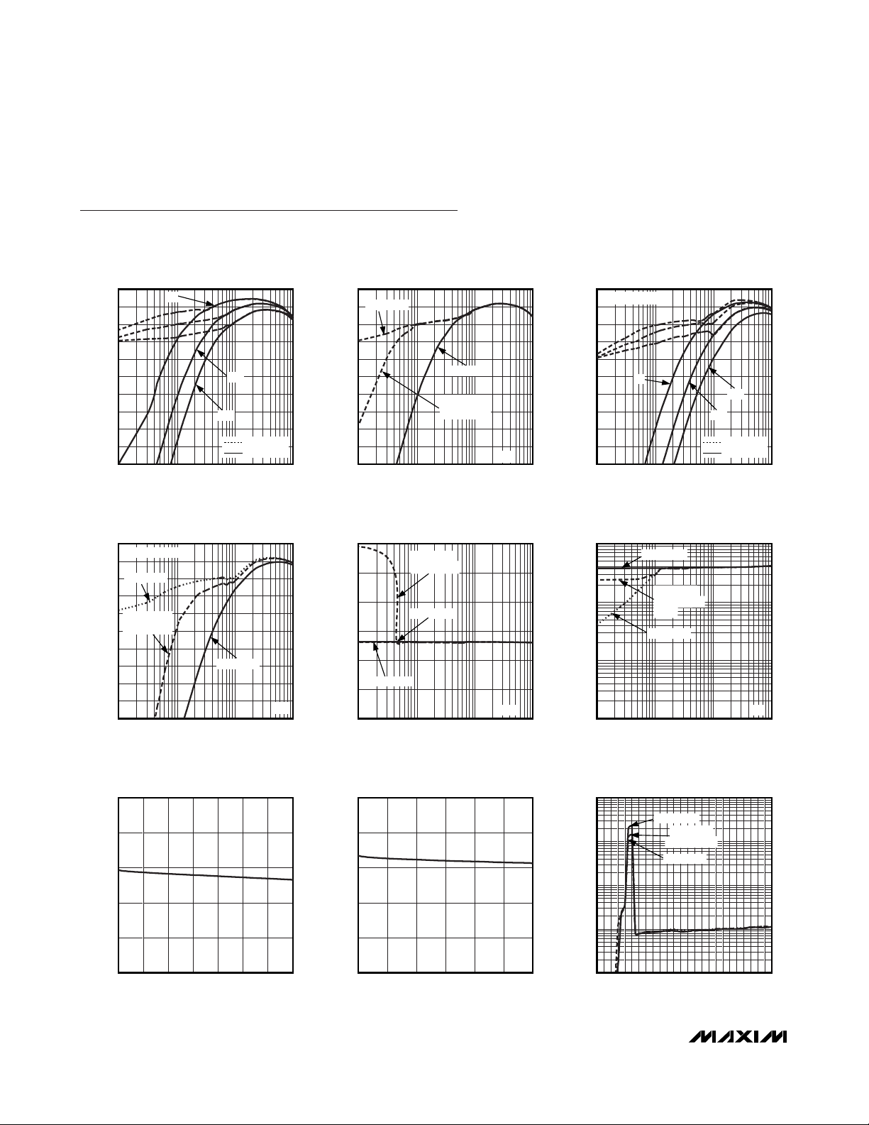
Typical Operating Characteristics
(Circuit of Figure 1, VIN= 12V, VDD= VCC= 5V, TON = REF, TA= +25°C, unless otherwise noted.)
5V OUTPUT EFFICIENCY
vs. LOAD CURRENT
100
95
90
85
80
75
70
EFFICIENCY (%)
65
60
55
50
0.01 10
7V
LOAD CURRENT (A)
3.3V OUTPUT EFFICIENCY
vs. LOAD CURRENT
100
5V SMPS ENABLED
95
SKIP MODE
90
85
80
ULTRASONIC
75
70
EFFICIENCY (%)
65
60
55
50
MODE
0.01 10
LOAD CURRENT (A)
12V
20V
SKIP MODE
PWM MODE
10.1
PWM MODE
10.1
12V
100
SKIP MODE
95
MAX17020 toc01
90
85
80
75
70
EFFICIENCY (%)
65
60
55
50
0.01 10
SMPS OUTPUT VOLTAGE DEVIATION
3
MAX17020 toc04
2
1
0
-1
SKIP MODE
OUTPUT VOLTAGE DEVIATION (%)
-2
-3
0.01 10
5V OUTPUT EFFICIENCY
vs. LOAD CURRENT
PWM MODE
ULTRASONIC
MODE
10.1
LOAD CURRENT (A)
vs. LOAD CURRENT
LOW-NOISE
ULTRASONIC
PWM MODE
10.1
LOAD CURRENT (A)
12V
12V
100
5V SMPS ENABLED
95
MAX17020 toc02
90
85
80
75
70
EFFICIENCY (%)
65
60
55
50
0.01 10
1000
MAX17020 toc05
100
10
SWITCHING FREQUENCY (kHz)
1
0.01 10
3.3V OUTPUT EFFICIENCY
vs. LOAD CURRENT
7V
20V
12V
SKIP MODE
PWM MODE
10.1
LOAD CURRENT (A)
SWITCHING FREQUENCY
vs. LOAD CURRENT
PWM MODE
LOW-NOISE
ULTRASONIC
MODE
SKIP MODE
10.1
LOAD CURRENT (A)
MAX17020 toc03
MAX17020 toc06
12V
5V LDO OUTPUT VOLTAGE
vs. LOAD CURRENT
5.2
5.1
5.0
4.9
OUTPUT VOLTAGE (V)
4.8
4.7
020 140
LOAD CURRENT (mA)
100 12040 60 80
MAX17020 toc07
OUTPUT VOLTAGE (V)
3.3V RTC OUTPUT VOLTAGE
vs. LOAD CURRENT
3.5
3.4
3.3
3.2
3.1
3.0
02 12
LOAD CURRENT (mA)
10468
MAX17020 toc08
NO-LOAD INPUT SUPPLY CURRENT
vs. INPUT VOLTAGE
100
PWM MODE
10
SKIP MODE
1
SUPPLY CURRENT (mA)
0.1
0.01
025
INPUT VOLTAGE (V)
LOW-NOISE
ULTRASONIC
15 20510
MAX17020 toc09
Page 11
MAX17020
Dual Quick-PWM Step-Down Controller
with Low-Power LDO, RTC Regulator
______________________________________________________________________________________ 11
Typical Operating Characteristics (continued)
(Circuit of Figure 1, VIN= 12V, VDD= VCC= 5V, TON = REF, TA= +25°C, unless otherwise noted.)
STANDBY AND SHUTDOWN INPUT
SUPPLY CURRENT vs. INPUT VOLTAGE
1
STANDBY (ONLDO = VIN)
0.1
SUPPLY CURRENT (mA)
SHUTDOWN
(ONLDO = ON1 = ON2 = GND)
0.01
025
INPUT VOLTAGE (V)
15 20510
70
60
MAX17020 toc10
50
40
30
SAMPLE PERCENTAGE (%)
20
10
0
-20 -4-12 4 12 20
100mV ILIM THRESHOLD
VOLTAGE DISTRIBUTION
50
+85°C
+25°C
40
30
20
SAMPLE PERCENTAGE (%)
10
0
90 9894 102 106 110
ILIM THRESHOLD VOLTAGE (mV)
SAMPLE SIZE = 150
12V
MAX17020 toc13
0V
0V
0V
0V
REFERENCE OFFSET
VOLTAGE DISTRIBUTION
+85°C
+25°C
2V REF OFFSET VOLTAGE (mV)
LDO AND RTC POWER-UP
A. INPUT SUPPLY, 5V/div
B. 5V LDO, 2V/div
200μs/div
SAMPLE SIZE = 150
MAX17020 toc14
C. 3.3V RTC, 2V/div
D. 2.0V REF, 1V/div
70
60
MAX17020 toc11
50
40
30
SAMPLE PERCENTAGE (%)
20
10
0
A
12V
12V
B
5V
C
3.3V
D
2.0V
5V
3.3V
2V
REFIN2 OFFSET
VOLTAGE DISTRIBUTION
+85°C
+25°C
-5 -1-3 1 3 5
REFIN2 OFFSET VOLTAGE (mV)
LDO AND RTC POWER REMOVAL
A. INPUT SUPPLY, 5V/div
B. 5V LDO, 2V/div
SAMPLE SIZE = 150
200μs/div
MAX17020 toc15
C. 3.3V RTC, 2V/div
D. 2.0V REF, 1V/div
MAX17020 toc12
A
12V
B
5V
C
3.3V
D
2.0V
Page 12

MAX17020
Dual Quick-PWM Step-Down Controller
with Low-Power LDO, RTC Regulator
12 ______________________________________________________________________________________
Typical Operating Characteristics (continued)
(Circuit of Figure 1, VIN= 12V, VDD= VCC= 5V, TON = REF, TA= +25°C, unless otherwise noted.)
5V LDO LOAD TRANSIENT
5V
0.1A
0A
A. LDO OUTPUT,
100mV/div
4μs/div
5V
0V
5V
MAX17020 toc16
A
B
B. LOAD CURRENT,
100mA/div
SHUTDOWN WAVEFORMS
(SWITCHING REGULATORS)
5V SMPS STARTUP AND SHUTDOWN
5V
5V
0V
5V
0V
A. 5V LDO OUTPUT, 0.2V/div
B. 5V SMPS OUTPUT, 2V/div
C. ON1, 5V/div
MAX17020 toc19
A
200μs/div
3.1A
0A
MAX17020 toc17
A
5V
B
5V
C
5V SMPS LOAD TRANSIENT
(PWM MODE)
(SWITCHING REGULATORS)
5V
0V
5V
5V
0V
0V
0A
A. ON1, 2V/div
B. 5V SMPS OUTPUT,
2V/div
STARTUP WAVEFORMS
100μs/div
C. PGOOD1, 5V/div
D. INDUCTOR CURRENT,
5A/div
MAX17020 toc20
A
MAX17020 toc18
A
B
5V
C
D
5V
0V
5V
0V
0A
A. ON1, 5V/div
B. 5V SMPS OUTPUT,
2V/div
200μs/div
C. PGOOD1, 2V/div
D. INDUCTOR CURRENT,
5A/div
B
C
D
0A
A. LOAD CURRENT, 2A/div
B. 5V SMPS OUTPUT, 100mV/div
C. INDUCTOR CURRENT, 2A/div
40μs/div
B
C
Page 13

MAX17020
Dual Quick-PWM Step-Down Controller
with Low-Power LDO, RTC Regulator
______________________________________________________________________________________ 13
Typical Operating Characteristics (continued)
(Circuit of Figure 1, VIN= 12V, VDD= VCC= 5V, TON = REF, TA= +25°C, unless otherwise noted.)
Pin Description
3.3V SMPS LOAD TRANSIENT
6.5A
0.5A
3.3V
0A
A. LOAD CURRENT, 5A/div
B. 3.3V SMPS OUTPUT, 100mV/div
C. INDUCTOR CURRENT, 5A/div
40μs/div
MAX17020 toc21
7V
A
5V
B
C
5V
5V
A. INPUT VOLTAGE, 5V/div
B. 5V LDO OUTPUT, 2V/div
PIN NAME FUNCTION
2V Reference-Voltage Output. Bypass REF to AGND with a 0.1µF or greater ceramic capacitor. The
1 REF
reference can source up to 50µA for external loads. Loading REF degrades output-voltage accuracy
according to the REF load-regulation error. The reference shuts down when ON1, ON2, and ONLDO are all
pulled low.
POWER REMOVAL
(SMPS UVLO RESPONSE)
10ms/div
MAX17020 toc22
A
B
C
D
C. 5V SMPS, 2V/div
D. PGOOD1, 5V/div
Switching-Frequency Setting Input. Select the OUT1/OUT2 switching frequencies by connecting TON as
follows for:
2 TON
High (V
Open (REF) = 400kHz/300kHz
GND = 400kH z/500kHz
3 V
CC
4 ONLDO
Analog Supply Voltage Input. Connect VCC to the system supply voltage with a series 50 resistor, and
bypass to analog ground using a 1µF or greater ceramic capacitor.
Enable Input for LDO. Drive ONLDO high to enable the linear regulator (LDO) output. Drive ONLDO low to
shut down the linear regulator output.
3.3V Always-On Linear Regulator Output for RTC Power. Bypass RTC with a 1µF or greater ceramic
5 RTC
capacitor to analog ground. RTC can source at lea st 5mA for external load s upport. RTC power-up is
required for controller operation.
Power-Input Supply. IN powers the linear regulators (RTC and LDO) and senses the input voltage for the
6 IN
Quick-PWM on-time one-shot timers. The high-side MOSFET’s on-time is inversely proportional to the input
voltage. Bypass IN with a 0.1μF or greater ceramic capacitor to PGND close to the MAX17020.
Linear Regulator Output. Bypa ss LDO with a 4.7µF or greater ceramic capacitor. LDO can source at lea st
7 LDO
100mA for external load support. LDO is powered from IN and its regulation threshold is set by LDOREFIN.
For preset 5V operation, connect LDOREFIN directl y to GND. For preset 3.3V operation, connect LDOREFIN
directly to V
) = 200kHz/300kHz
CC
. When LDO is used for 5V operation, LDO must supply VCC and VDD.
CC
Page 14

MAX17020
Dual Quick-PWM Step-Down Controller
with Low-Power LDO, RTC Regulator
14 ______________________________________________________________________________________
Pin Description (continued)
PIN NAME FUNCTION
External Reference Input for the Linear Regulator. LDOREFIN sets the LDO regulation voltage (V
V
8 LDOREFIN
9 BYP
10 OUT1
11 FB1
12 ILIM1
13 PGOOD1
14 ON1 Enable Input for SMPS1. Drive ON1 high to enable SMPS1. Drive ON1 low to shut down SMPS1.
15 DH1 High-Side Gate-Driver Output for SMPS1. DH1 swings from LX1 to BST1.
16 LX1
17 BST1
18 DL1 Low-Side Gate-Driver Output for SMPS1. DL1 swings from PGND to V
19 V
20 SECFB
21 AGND Analog Ground. Connect the backside exposed pad to AGND.
22 PGND Power Ground
23 DL2 Low-Side Gate-Driver Output for SMPS2. DL2 swings from PGND to V
24 BST2
25 LX2
DD
LDOR EFI N
output voltage, or connect LDOREFIN to V
to 5V and is enabled, LDO must supply V
Linear Regulator Bypass Input. When BYP voltage exceeds 93.5% of the LDO voltage, the controller
bypasses the LDO output to the BYP input. The bypass switch is disabled if the LDO voltage drops by 8.5%
from its nominal regulation threshold. When not being used, connect BYP to GND.
Output Voltage-Sense Input for SMPS1. OUT1 is an input to the Quick-PWM on-time one-shot timer. OUT1 also
serves as the feedback input for the preset 5V (FB1 = GND) and 1.5V (FB1 = V
Adjustable Feedback Voltage-Sense Connection for SMPS1. Connect FB1 to GND for fixed 5V operation.
Connect FB1 to V
to analog ground to ad just the output voltage between 0.7V and 5.5V.
Valley Current-Limit Adjustment for SMPS1. The GND - LX1 current-limit threshold is 1/10 the voltage present
on ILIM1 over a 0.2V to 2V range. An internal 5µA current source allows this voltage to be set with a single
resistor between ILIM1 and analog ground.
Open-Drain Power-Good Output for S MPS1. PGOOD1 is low when the output voltage is more than 16% ( typ) below
the nominal regulation threshold, during soft-start, in shutdown, and after the fault latch has been tripped. After the
soft-start circuit has terminated, PGOOD1 becomes high impedance if the output is in regulation.
Inductor Connection for SMPS1. Connect LX1 to the switched side of the inductor. LX1 is the lower supply rail
for the DH1 high-side gate driver.
Boost Flying-Capacitor Connection for SMPS1. Connect to an external capacitor as shown in Figure 1. An
optional resistor in series with BST1 allows the DH1 turn-on current to be adjusted.
Supply-Voltage Input for the DL_ Gate Drivers. Connect to a 5V supply. Also connect to the drain of the BST
diode switch.
Secondary Feedback Input. The secondary feedback input forces the SMPS1 output into ultrasonic mode
when the SECFB voltage drops below its 2V threshold voltage. This forces DL1 and DH1 to switch, allowing
the system to refresh an external low-power charge pump being driven by DL1 (see Figure 1). Connect
SECFB to V
Boost Flying-Capacitor Connection for SMPS2. Connect to an external capacitor as shown in Figure 1. An
optional resistor in series with BST2 allows the DH2 turn-on current to be adjusted.
Inductor Connection for SMPS2. Connect LX2 to the switched side of the inductor. LX2 is the lower supply rail
for the DH2 high-side gate driver.
) for a 0.3V to 2V LDOREFIN range. Connect LDOREFIN to GND for a fixed 5V linear-regulator
for a fixed 3.3V linear-regulator output voltage. When LDO is set
CC
and VDD.
CC
CC
for fixed 1.5V operation. Connect FB1 to an external resistive voltage-divider from OUT1
CC
DD.
to the 5V bias supply to disable secondary feedback.
CC
DD.
= 2 x
LDO
) output voltage settings.
Page 15

MAX17020
Dual Quick-PWM Step-Down Controller
with Low-Power LDO, RTC Regulator
______________________________________________________________________________________ 15
Pin Description (continued)
PIN NAME FUNCTION
26 DH2 High-Side Gate-Driver Output for SMPS2. DH2 swings from LX2 to BST2.
27 ON2 Enable Input for SMPS2. Drive ON2 high to enable SMPS2. Drive ON2 low to shut down SMPS2.
Open-Drain Power-Good Output for SMPS2. PGOOD2 is low when the output voltage is more than 150mV
(typ) below the REFIN2 voltage or more than 16% below the preset voltage, during soft-start, in shutdown,
28 PGOOD2
29 SKIP
30 OUT2
31 ILIM2
32 REFIN2
— EP Exposed Pad. Connect the backside exposed pad to AGND.
and when the fault latch has been tripped. After the soft-start circuit has terminated, PGOOD2 becomes high
impedance if the output is in regulation. PGOOD2 is blanked—forced high-impedance state—when a
dynamic REFIN transition is detected.
Pulse-skipping Control Input. This three-level input determines the operating mode for the switching
regulators:
High (VCC) = Forced-PWM operation
Open/REF (2V) = Ultrasonic mode
GND = Pulse-skipping mode
Output Voltage-Sense Input for SMPS2. OUT2 is an input to the Quick-PWM on-time one-shot timer. OUT2
also serves as the feedback input for the preset 3.3V (REFIN2 = V
Valley Current-Limit Adjustment for SMPS2. The GND - LX2 current-limit threshold is 1/10 the voltage present
on ILIM2 over a 0.2V to 2V range. An internal 5µA current source allows this voltage to be set with a single
resistor between ILIM2 and analog ground.
External Reference Input for SMPS2. REFIN2 sets the feedback-regulation voltage (V
MAX17020 includes an internal window comparator to detect when the REFIN2 voltage changes, allowing the
controller to blank PGOOD2 and the fault protection. Connect REFIN2 to RTC for fixed 1.05V operation.
Connect REFIN2 to V
for fixed 3.3V operation.
CC
) and 1.05V (REFIN2 = RTC).
CC
= V
OUT2
REFIN2
). The
Page 16

MAX17020
Dual Quick-PWM Step-Down Controller
with Low-Power LDO, RTC Regulator
16 ______________________________________________________________________________________
Figure 1. Standard Application Circuit—Main Supply
NOTE: PLACE C22 BETWEEN
IN AND PGND AS CLOSE AS
POSSIBLE TO THE MAX17020.
5V OUTPUT
C
OUT1
12V TO 15V
CHARGE
PUMP
C8
0.1μF
C6
0.1μF
500kΩ
L1
D1
D
X1
R4
D
X2
R5
100kΩ
N
H1
C
BST1
0.1μF
N
L1
C5
10nF
C7
10nF
C22
0.1μF
DH1
BST1
LX1
DL1
OUT1
BYP
MAX17020
SECFB
FB1
IN
DH2
BST2
LX2
DL2
PGND
AGND
OUT2
PGOOD1
PGOOD2
RTC
REF
SKIP
C4
0.1μF
RGND
100kΩ
C3
1μF
0Ω
R6
N
H2
C
BST2
0.1μF
N
L2
R7
100kΩ
C
IN
4 x 10μF 25V
L2
D2
)*
INPUT (V
IN
7V TO 24V
3.3V OUTPUT
C
OUT2
5V SMPS OUTPUT (OUT1)
POWER-GOOD
}
RTC SUPPLY
LDOREFIN
V
DD
5V LDO OUTPUT
POWER GROUND
ANALOG GROUND
*LOWER INPUT VOLTAGES REQUIRE
ADDITIONAL INPUT CAPACITANCE. IF
OPERATING NEAR DROPOUT, COMPONENT
SELECTION MUST BE CAREFULLY DONE TO
ENSURE PROPER OPERATION.
47Ω
1.0μF
C1
R1
C2
4.7μF
LDO
V
CC
REFIN2
R
ILIM1
ILIM1
PAD
ON1
ON2
ONLDO
TON
ILIM2
OFFON
OUT1/OUT2 SWITCHING FREQUENCY
X
OPEN (REF): 400kHz/300kHz
R
ILIM2
Page 17

MAX17020
Dual Quick-PWM Step-Down Controller
with Low-Power LDO, RTC Regulator
______________________________________________________________________________________ 17
Figure 2. Functional Diagram Overview
IN
TON
SKIP
RTC
SECFB
ILIM1
OUT1
BST1
DH1
LX1
DL1
PGND
FB1
ON1
PGOOD1
ONLDO
5V LINEAR
REGULATOR
3.3V LINEAR
REGULATOR
V
DD
PWM1
CONTROLLER
(FIGURE 3)
V
DD
FB SELECT
(PRESET vs. ADJ)
UVLO
POWER-GOOD
AND FAULT
PROTECTION
FAULT1
LDO BYPASS
CIRCUITRY
CONTROLLER
(FIGURE 3)
FAULT2
POWER-GOOD
AND FAULT
PROTECTION
PWM2
FB SELECT
(PRESET vs. ADJ)
UVLO
V
DD
LDOREFIN
LDO
BYP
ILIM2
OUT2
V
DD
BST2
DH2
LX2
DL2
REFIN2
ON2
PGOOD2
PAD
MAX17020
REF
V
CC
REF
2V
GND
Page 18

MAX17020
Dual Quick-PWM Step-Down Controller
with Low-Power LDO, RTC Regulator
18 ______________________________________________________________________________________
Table 1. Component Selection for Standard Applications
Table 2. Component Suppliers
400kHz/300kHz
COMPONENT
Input Voltage VIN = 7V to 24V VIN = 7V to 24V VIN = 7V to 24V
Input Capacitor
)
(C
IN
SMPS 1
Output Capacitor
)
(C
OUT1
Inductor
(L1)
High-Side MOSFET
(N
)
H1
Low-Side MOSFET
(N
)
L1
Current-Limit Resistor
(R
)
ILIM1
SMPS 2
Output Capacitor
)
(C
OUT2
Inductor
(L2)
High-Side MOSFET
)
(N
H2
Low-Side MOSFET
)
(N
L2
Current-Limit Resistor
)
(R
ILIM2
SMPS 1: 5V AT 5A
SMPS 2: 3.3V AT 8A
(4x) 10μF, 25V
Taiyo Yuden TMK432BJ106KM
330μF, 6V, 18mΩ
SANYO 6TPE330MIL
4.3μH, 11.4mΩ, 11A
Sumida CEP125U
Fairchild Semiconductor
FDS6612A
26mΩ/30mΩ, 30V
Fairchild Semiconductor
FDS6670S
9mΩ/11.5mΩ, 30V
200kΩ 150kΩ 49.9kΩ
470μF, 4V, 15mΩ
SANYO 4TPE470MFL
4.3μH, 11.4mΩ, 11A
Sumida CEP125U
Fairchild Semiconductor
FDS8690
8.6mΩ/11.4mΩ, 30V
Fairchild Semiconductor
FDMS8660S
2.6mΩ/3.5mΩ, 30V
200kΩ 200kΩ 49.9kΩ
400kHz/500kHz
SMPS 1: 5V AT 3A
SMPS 2: 3.3V AT 5A
(2x) 10μF, 25V
Taiyo Yuden TMK432BJ106KM
330μF, 6V, 18mΩ
SANYO 6TPE330MIL
4.7μH, 9.8mΩ, 7A
Sumida CDRH10D68
Vishay Siliconix
Si4814DY
Dual 30V MOSFET
High side: 19mΩ/23mΩ
Low side: 18mΩ/22mΩ
330μF, 6V, 18mΩ
SANYO 6TPE330MIL
4.7μH, 9.8mΩ, 7A
Sumida CDRH10D68
Vishay Siliconix
Si4814DY
Dual 30V MOSFET
High side: 19mΩ/23mΩ
Low side: 18mΩ/22mΩ
(4x) 10μF, 25V
Taiyo Yuden TMK432BJ106KM
(2x) 330μF, 2V, 7mΩ
SANYO 2TPF330M7
1.5μH, 12A, 7mΩ
NEC/Tokin MPLC1040L1R5
Fairchild Semiconductor
FDS8690
8.6mΩ/11.4mΩ, 30V
Fairchild Semiconductor
FDMS8660S
2.6mΩ/3.5mΩ, 30V
330μF, 2V, 7mΩ
SANYO 2TPF330M7
1.5μH, 12A, 7mΩ
NEC/Tokin MPLC1040L1R5
Fairchild Semiconductor
FDS8690
8.6mΩ/11.4mΩ, 30V
Fairchild Semiconductor
FDMS8660S
2.6mΩ/3.5mΩ, 30V
400kHz/300kHz
SMPS 1: 1.5V AT 8A
SMPS 2: 1.05V AT 5A
SUPPLIER WEBSITE
AVX Corp. www.avxcorp.com
C entr al S emi cond uctor Cor p . www.centralsemi.com
Fairchild Semiconductor www.fairchildsemi.com
International Rectifier www.irf.com
KEMET Corp www.kemet.com
NEC/Tokin America, Inc. www.nec-tokinamerica.com
Panasonic Corp. www.panasonic.com
Philips/nxp Semiconductor www.semiconductors.philips.com
Pulse Engineering www.pulseeng.com
SUPPLIER WEBSITE
Renesas Technol og y C or p . www.renesas.com
SANYO Electric Co., Ltd. www.sanyodevice.com
Sumida Corp. www.sumida.com
Taiyo Yuden www.t-yuden.com
TDK Corp. www.component.tdk.com
TOKO America, Inc. www.tokoam.com
Vishay (Dale, Siliconix) www.vishay.com
Würth Elektronik GmbH &
Co. KG
www.we-online.com
Page 19

MAX17020
Dual Quick-PWM Step-Down Controller
with Low-Power LDO, RTC Regulator
______________________________________________________________________________________ 19
Detailed Description
The MAX17020 step-down controller is ideal for highvoltage, low-power supplies for notebook computers.
Maxim’s Quick-PWM pulse-width modulator in the
MAX17020 is specifically designed for handling fast
load steps while maintaining a relatively constant operating frequency and inductor operating point over a
wide range of input voltages. The Quick-PWM architecture circumvents the poor load-transient timing problems of fixed-frequency current-mode PWMs, while also
avoiding the problems caused by widely varying
switching frequencies in conventional constant-on-time
and constant-off-time PWM schemes. Figure 2 is a
functional diagram overview. Figure 3 is the functional
diagram—Quick-PWM core.
The MAX17020 includes several features for multipurpose notebook functionality, allowing this controller to
be used two or three times in a single notebook—main,
I/O chipset, and graphics. The MAX17020 includes a
100mA LDO that can be configured for preset 5V operation—ideal for initial power-up of the notebook and
main supply—or can be adjusted for lower voltage
operation—ideal for low-power I/O or graphics supply
requirements. Additionally, the MAX17020 includes a
3.3V, 5mA RTC supply that remains always enabled,
which can be used to power the RTC supply and system pullups when the notebook shuts down. The
MAX17020 also includes an optional secondary feedback input that allows an unregulated charge pump or
secondary winding to be included on a supply—ideal
for generating the low-power 12V to 15V load switch
supply. Finally, the MAX17020 includes a reference
input on SMPS 2 that allows dynamic voltage transitions
when driven by an adjustable resistive voltage-divider or
DAC—ideal for the dynamic graphics core requirements.
3.3V RTC Power
The MAX17020 includes a low-current (5mA) linear regulator that remains active as long as the input supply
(IN) exceeds 2V (typ). The main purpose of this
“always-enabled” linear regulator is to power the realtime clock (RTC) when all other notebook regulators are
disabled. RTC also serves as the main bias supply of
the MAX17020 so it powers up before the LDO and
switching regulators. The RTC regulator sources at
least 5mA for external loads.
Adjustable 100mA Linear Regulator
The MAX17020 includes a high-current (100mA) linear
regulator that can be configured for preset 5V or 3.3V
operation or adjusted between 0.6V to 4V. When the
MAX17020 is configured as a main supply, this LDO is
required to generate the 5V bias supply necessary to
power up the switching regulators. Once the switching
regulators are enabled, the LDO can be bypassed
using the dedicated BYP input. The adjustable linear
regulator allows generation of the 3.3V suspend supply
or buffered low-power chipset and GPU reference supplies. The MAX17020 LDO sources at least 100mA of
supply current.
Bypass Switch
The MAX17020 includes an independent LDO bypass
input that allows the LDO to be bypassed by either
switching regulator output or from a different regulator all
together. When the bypass voltage (BYP) exceeds 93.5%
of the LDO output voltage for 500μs, the MAX17020
reduces the LDO regulation threshold and turns on an
internal p-channel MOSFET to short BYP to LDO. Instead
of disabling the LDO when the MAX17020 enables the
bypass switch, the controller reduces the LDO regulation
voltage, which effectively places the linear regulator in a
standby state while switched over, yet allows a fast
recovery if the bypass supply drops.
Connect BYP to GND when not used to avoid unintentional conduction through the body diode (BYP to LDO)
of the p-channel MOSFET.
5V Bias Supply (VCC/VDD)
The MAX17020 requires an external 5V bias supply
(VDDand VCC) in addition to the battery. Typically, this
5V bias supply is generated by either the internal
100mA LDO (when configured for a main supply) or
from the notebook’s 95%-efficient 5V main supply (when
configured for an I/O chipset, DDR, or graphics).
Keeping these bias supply inputs independent
improves the overall efficiency and allows the internal
linear regulator to be used for other applications as well.
The VDDbias supply input powers the internal gate drivers and the VCCbias supply input powers the analog
control blocks. The maximum current required is dominated by the switching losses of the drivers and can be
estimated as follows:
I
BIAS(MAX)
= I
CC(MAX)
+ fSWQG≈ 30mA to 60mA (typ)
Page 20

MAX17020
Dual Quick-PWM Step-Down Controller
with Low-Power LDO, RTC Regulator
20 ______________________________________________________________________________________
Free-Running Constant-On-Time PWM
Controller with Input Feed-Forward
The Quick-PWM control architecture is a pseudo-fixedfrequency, constant on-time, current-mode regulator
with voltage feed-forward. This architecture relies on
the output filter capacitor’s ESR to act as a currentsense resistor, so the feedback ripple voltage provides
the PWM ramp signal. The control algorithm is simple:
the high-side switch on-time is determined solely by a
one-shot whose pulse width is inversely proportional to
input voltage and directly proportional to output voltage. Another one-shot sets a minimum off-time (400ns
typ). The on-time one-shot is triggered if the error comparator is low, the low-side switch current is below the
valley current-limit threshold, and the minimum off-time
one-shot has timed out.
On-Time One-Shot
The heart of the PWM core is the one-shot that sets the
high-side switch on-time. This fast, low-jitter, adjustable
one-shot includes circuitry that varies the on-time in
response to battery and output voltage. The high-side
switch on-time is inversely proportional to the battery
voltage as sensed by the IN input, and proportional to
the output voltage:
On-Time = K (V
OUT/VIN
)
where K (switching period) is set by the tri-level TON
input (see the
Pin Description
section). High-frequency
(400kHz/500kHz) operation optimizes the application
for the smallest component size, trading off efficiency
due to higher switching losses. This might be acceptable in ultra-portable devices where the load currents
are lower and the controller is powered from a lower
voltage supply. Low-frequency (200kHz/300kHz) operation offers the best overall efficiency at the expense of
component size and board space.
For continuous conduction operation, the actual switching
frequency can be estimated by:
where V
DROP1
is the sum of the parasitic voltage drops
in the inductor discharge path, including synchronous
rectifier, inductor, and PCB resistances; V
DROP2
is the
sum of the voltage drops in the charging path, including the high-side switch, inductor, and PCB resistances; and tONis the on-time calculated by the
MAX17020.
Table 3. Approximate K-Factor Errors
VV
f
SW
+
=
tVV V
ON IN DROP DROP
OUT DROP
+−
()
1
12
SWITCHING
REGULATOR
SMPS 1
SMPS 2
TON SETTING
(kHz)
200kHz
TON = V
TON = REF or GND
TON = REF or V
TON = GND
CC
400kHz
300kHz
CC
500kHz
TYPICAL K-FACTOR
(µs)
5.0 ±10 Use for absolute best efficiency.
2.5 ±12.5
3.3 ±10
2.0 ±12.5
K-FACTOR ERROR
(%)
COMMENTS
Useful in 3-cell systems for lighter loads
than the CPU core or where size is key.
Considered mainstream by current
standards.
Good operating point for compound buck
designs or desktop circuits.
Page 21

MAX17020
Dual Quick-PWM Step-Down Controller
with Low-Power LDO, RTC Regulator
______________________________________________________________________________________ 21
Figure 3. Functional Diagram—Quick-PWM Core
INTEGRATOR
REF
AGND
LX
ILIM
VCC
NEG CURRENT
LIMIT
VALLEY
CURRENT LIMIT
GND
AGND
SLOPE COMP
t
OFF(MIN)
TRIG
Q
ONE-SHOT
S
R*
* RESET DOMINATE
Q
ONE-SHOT
ON-TIME
COMPUTE
INT PRESET
OR EXT ADJ
ANALOG
SOFT-
START/STOP
Q DH DRIVER
t
ON
TRIG
FB
REFIN
ON
TON
IN
ZERO
CROSSING
GND
ULTRASONIC
THRESHOLD
GND
SKIP
FB
REFIN
THREE-LEVEL
DECODE
ULTRASONIC
Q
ONE-SHOT
S
R
TRIG
Q
DL DRIVER
Page 22

MAX17020
Dual Quick-PWM Step-Down Controller
with Low-Power LDO, RTC Regulator
22 ______________________________________________________________________________________
Modes of Operation
Forced-PWM Mode (
SSKKIIPP
= VCC)
The low-noise forced-PWM mode (SKIP = VCC) disables the zero-crossing comparator, which controls the
low-side switch on-time. This forces the low-side gatedrive waveform to constantly be the complement of the
high-side gate-drive waveform, so the inductor current
reverses at light loads while DH maintains a duty factor
of V
OUT/VIN
. The benefit of forced-PWM mode is to
keep the switching frequency fairly constant. However,
forced-PWM operation comes at a cost: the no-load 5V
bias current remains between 20mA to 60mA depending on the switching frequency and MOSFET selection.
The MAX17020 automatically uses forced-PWM operation during all transitions—dynamic REFIN, startup, and
shutdown—regardless of the SKIP configuration.
Automatic Pulse-Skipping Mode (
SSKKIIPP
= GND)
In skip mode (SKIP = GND), an inherent automatic
switchover to PFM takes place at light loads. This
switchover is affected by a comparator that truncates
the low-side switch on-time at the inductor current’s
zero crossing. The zero-crossing comparator threshold
is set by the differential across LX and AGND.
DC output-accuracy specifications refer to the integrated threshold of the error comparator. When the inductor
is in continuous conduction, the MAX17020 regulates
the valley of the output ripple and the internal integrator
removes the actual DC output-voltage error caused by
the output-ripple voltage and internal slope compensation. In discontinuous conduction (SKIP = GND and
I
OUT
< I
LOAD(SKIP)
), the integrator cannot correct for
the low-frequency output ripple error, so the output voltage has a DC regulation level higher than the error
comparator threshold by approximately 1.5% due to
slope compensation and output ripple voltage.
Ultrasonic Mode (
SSKKIIPP
= Open or REF)
Leaving SKIP unconnected or connecting SKIP to REF
(2V) activates a unique pulse-skipping mode with a
guaranteed minimum switching frequency of 20kHz.
This ultrasonic pulse-skipping mode eliminates audiofrequency modulation that would otherwise be present
when a lightly loaded controller automatically skips
pulses. In ultrasonic mode, the controller automatically
transitions to fixed-frequency PWM operation when the
load reaches the same critical conduction point
(I
LOAD(SKIP)
) that occurs when normally pulse skipping.
An ultrasonic pulse occurs (Figure 4) when the controller detects that no switching has occurred within the
last 37μs or when SECFB drops below its feedback
threshold. Once triggered, the ultrasonic circuitry pulls
DL high, turning on the low-side MOSFET to induce a
negative inductor current. After the inductor current
reaches the negative ultrasonic current threshold, the
controller turns off the low-side MOFET (DL pulled low)
and triggers a constant on-time (DH driven high). When
the on-time has expired, the controller reenables the
low-side MOSFET until the inductor current drops below
the zero-crossing threshold. Starting with a DL pulse
greatly reduces the peak output voltage when compared to starting with a DH pulse.
The output voltage at the beginning of the ultrasonic
pulse determines the negative ultrasonic current threshold, resulting in the following equation:
V
NEG(US)
= ILRCS= (V
NOM
- VFB) x 0.385V
where V
NOM
is the nominal feedback-regulation voltage, and VFBis the actual feedback voltage (VFB>
V
NOM
), and RCSis the current-sense resistance seen
across LX to AGND.
Secondary Feedback: SECFB—OUT1 ONLY
When the controller skips pulses (SKIP = GND or REF),
the long time between pulses (especially if the output is
sinking current) allows the external charge-pump voltage
or transformer secondary winding voltage to drop. When
the SECFB voltage drops below its 2V feedback threshold, the MAX17020 issues an ultrasonic pulse (regardless
of the ultrasonic one-shot state). This forces a switching
cycle, allowing the external unregulated charge pump (or
transformer secondary winding) to be refreshed. See the
Ultrasonic Mode (SKIP = Open or REF)
section for
switching cycle sequence/specifications.
Figure 4. Ultrasonic Waveforms
37μs (typ)
INDUCTOR
CURRENT
ZERO-CROSSING
DETECTION
0
I
SONIC
ON-TIME (tON)
Page 23

MAX17020
Dual Quick-PWM Step-Down Controller
with Low-Power LDO, RTC Regulator
______________________________________________________________________________________ 23
Dynamic Output Voltage—OUT2 Only
The MAX17020 regulates OUT2 to the voltage set at
REFIN2, so the MAX17020 supports applications that
require dynamic output-voltage changes between two
set points by adjusting the REFIN2 voltage. For a stepvoltage change at REFIN2, the rate of change of the
output voltage is limited either by the internal slew-rate
circuit, by the REFIN2 slew rate, or by the component
selection—inductor current ramp, the total output
capacitance, the current limit, and the load during the
transition—whichever is the slowest. The total output
capacitance determines how much current is needed to
change the output voltage, while the inductor limits the
current ramp rate. Additional load current slows down
the output voltage change during a positive REFIN2
voltage change, and speeds up the output voltage
change during a negative REFIN2 voltage change.
Figure 5 is the dynamic REFIN transition.
Automatic Fault Blanking
When the MAX17020 automatically detects that the
internal target and REFIN2 are more than ±25mV (typ)
apart, the controller automatically blanks PGOOD2,
blanks the UVP protection, and sets the OVP threshold
to REF + 200mV. The blanking remains until 1) the internal target and REFIN2 are within ±20mV of each other
and 2) an edge is detected on the error amplifier signifying that the output is in regulation. This prevents the
system or internal fault protection from shutting down
the controller during transitions.
Valley Current-Limit Protection
The current-limit circuit employs a unique “valley” current-sensing algorithm that senses the inductor current
through the low-side MOSFET—across LX to AGND. If
the current through the low-side MOSFET exceeds the
valley current-limit threshold, the PWM controller is not
allowed to initiate a new cycle. The actual peak current
is greater than the valley current-limit threshold by an
amount equal to the inductor ripple current. Therefore,
the exact current-limit characteristic and maximum load
capability are a function of the inductor value and battery voltage. When combined with the undervoltage
protection circuit, this current-limit method is effective in
almost every circumstance.
In forced-PWM mode, the MAX17020 also implements
a negative current limit to prevent excessive reverse
inductor currents when V
OUT
is sinking current. The
negative current-limit threshold is set to approximately
120% of the positive current limit.
POR, UVLO
When VCCrises above the power-on reset (POR) threshold, the MAX17020 clears the fault latches, forces the
low-side MOSFET to turn on (DL high), and resets the
soft-start circuit, preparing the controller for power-up.
However, the V
CC
undervoltage lockout (UVLO) circuitry
inhibits switching until V
CC
reaches 4.2V (typ). When
VCCrises above 4.2V and the controller has been
enabled (ON_ pulled high), the controller activates the
enabled PWM controllers and initializes soft-start.
Figure 5. Dynamic REFIN Transition
REFIN
OUTPUT
VOLTAGE
LX
PGOOD
OVP
20mV
BLANK HIGH-Z
REF + 140mV
±20mV WINDOW BETWEEN
INTERNAL TARGET AND REFIN2
INTERNAL EA TARGET = ACTUAL V
EA TARGET + 140mV
DYNAMIC REFIN WINDOW
20mV
OUT
BLANK HIGH-Z
EA TARGET + 140mV
Page 24

MAX17020
Dual Quick-PWM Step-Down Controller
with Low-Power LDO, RTC Regulator
24 ______________________________________________________________________________________
When VCCdrops below the UVLO threshold (falling
edge), the controller stops switching, and DH and DL are
pulled low and a 10Ω switch discharges the outputs.
When the 2V POR falling-edge threshold is reached, the
DL state no longer matters since there is not enough voltage to force the switching MOSFETs into a low on-resistance state, so the controller pulls DL high, allowing a
soft discharge of the output capacitors (damped
response). However, if the VCCrecovers before reaching
the falling POR threshold, DL remains low until the error
comparator has been properly powered up and triggers
an on-time. Only one enable input needs to be toggled
to clear the fault latches and activate both outputs.
Soft-Start and Soft-Shutdown
The MAX17020 includes voltage soft-start and softshutdown—slowly ramping up and down the target voltage. During startup, the slew-rate control softly slews
the preset/fixed target voltage over a 1ms startup period or its tracking voltage (REFIN2 < 2V) with a 1mV/μs
slew rate. This long startup period reduces the inrush
current during startup.
When ON1 or ON2 is pulled low or the output undervoltage fault latch is set, the respective output automatically
enters soft-shutdown—the regulator enters PWM mode
and ramps down its preset/fixed output voltage over a
1ms period or its tracking voltage (REFIN2 < 2V) with a
1mV/μs slew rate. After the output voltage drops below
0.1V, the MAX17020 pulls DL high, clamping the output
and LX switching node to ground, preventing leakage
currents from pulling up the output and minimizing the
negative output voltage undershoot during shutdown.
Output Voltage
DC output-accuracy specifications in the
Electrical
Characteristics
table refer to the error comparator’s
threshold. When the inductor continuously conducts, the
MAX17020 regulates the valley of the output ripple, so
the actual DC output voltage is lower than the slope-compensated trip level by 50% of the output ripple voltage.
For PWM operation (continuous conduction), the output
voltage is accurately defined by the following equation:
where V
NOM
is the nominal feedback voltage, A
CCV
is
the integrator’s gain, and V
RIPPLE
is the output ripple
voltage (V
RIPPLE
= ESR x ΔI
INDUCTOR
, as described in
the
Output Capacitor Selection
section).
In discontinuous conduction (I
OUT
< I
LOAD(SKIP)
), the
longer off-times allow the slope compensation to
increase the threshold voltage by as much as 1%, so
the output voltage regulates slightly higher than it would
in PWM operation.
Internal Integrator
The internal integrator improves the output accuracy by
removing any output accuracy errors caused by the
slope compensation, output ripple voltage, and erroramplifier offset. Therefore, the DC accuracy (in forcedPWM mode) depends on the integrator’s gain, the integrator’s offset, and the accuracy of the integrator’s reference input.
Adjustable/Fixed Output Voltages
Connect FB1 to GND for fixed 5V operation. Connect
FB1 to VCCfor fixed 1.5V operation. Connect FB1 to an
external resistive voltage-divider from OUT1 to analog
ground to adjust the output voltage between 0.7V and
5.5V. During soft-shutdown, application circuits configured for adjustable feedback briefly switch modes when
FB1 drops below the 110mV dual-mode threshold.
Choose R
FBL
(resistance from FB1 to AGND) to be
approximately 49.9kΩ and solve for R
FBH
(resistance
from OUT1 to FB1) using the following equation:
Connect REFIN2 to VCCfor fixed 3.3V operation.
Connect REFIN2 to RTC (3.3V) for fixed 1.05V operation.
Connect REFIN2 to an external resistive voltage-divider
from REF to analog ground to adjust the output voltage
between 0V and 2V.
Choose R
REFINL
(resistance from REFIN2 to GND) to
be approximately 49.9kΩ and solve for R
REFINH
(resis-
tance from REF to REFIN2) using the equation:
Power-Good Outputs (PGOOD)
and Fault Protection
PGOOD is the open-drain output that continuously
monitors the output voltage for undervoltage and overvoltage conditions. PGOOD_ is actively held low in shutdown (ON_ = GND), during soft-start or soft-shutdown.
Approximately 20μs (typ) after the soft-start
terminates, PGOOD_ becomes high impedance as long
as the feedback voltage exceeds 85% of the nominal
fixed-regulation voltage or within 150mV of the REFIN2
input voltage. PGOOD_ goes low if the feedback voltage drops 16% below the fixed target voltage, or if the
output voltage drops 150mV below the dynamic REFIN2
voltage, or if the SMPS controller is shut down. For a
⎝
⎠
⎞
⎠
⎟
V
⎛
VV
OUT PWM NOM
=+
()
RIPPLE
⎜
⎝
2
A
CCV
V
RR
=× −
FBH FBL
RR
REFINH
=×−
REFINL
⎛
OUT
⎜
071.
⎛
⎜
⎝
V
V
V
1
REF
OUT
⎞
⎟
1
2
⎞
⎟
⎠
Page 25

MAX17020
Dual Quick-PWM Step-Down Controller
with Low-Power LDO, RTC Regulator
______________________________________________________________________________________ 25
logic-level PGOOD_ output voltage, connect an external
pullup resistor between PGOOD_ and VDD. A 100kΩ
pullup resistor works well in most applications.
Overvoltage Protection (OVP)
When the output voltage rises 16% above the fixed-regulation voltage or has risen 200mV above the dynamic
REFIN2 input voltage, the controller immediately pulls
the respective PGOOD_ low, sets the overvoltage fault
latch, and immediately pulls the respective DL_ high—
clamping the output to GND. Toggle either ON1 or ON2
input, or cycle VCCpower below its POR threshold to
clear the fault latch and restart the controller.
Undervoltage Protection (UVP)
When the output voltage drops 30% below the fixedregulation voltage or has dropped 300mV below the
dynamic REFIN2 input voltage, the controller immediately pulls the respective PGOOD_ low, sets the undervoltage fault latch, and begins the shutdown sequence.
After the output voltage drops below 0.1V, the synchronous rectifier turns on, clamping the output to GND.
Toggle either ON1 or ON2 input, or cycle VCCpower
below its POR threshold to clear the fault latch and
restart the controller.
Thermal-Fault Protection (TSHDN)
The MAX17020 features a thermal-fault protection circuit.
When the junction temperature rises above +160°C, a
thermal sensor activates the fault latch, pulls PGOOD1
and PGOOD2 low, enables the 10Ω discharge circuit,
and disables the controller—DH and DL are pulled low.
Toggle ONLDO or cycle IN power to reactivate the controller after the junction temperature cools by 15°C.
Design Procedure
Firmly establish the input-voltage range and maximum
load current before choosing a switching frequency and
inductor operating point (ripple-current ratio). The primary
design trade-off lies in choosing a good switching frequency and inductor operating point, and the following
four factors dictate the rest of the design:
• Input Voltage Range: The maximum value
(V
IN(MAX)
) must accommodate the worst-case, high
AC-adapter voltage. The minimum value (V
IN(MIN)
)
must account for the lowest battery voltage after
drops due to connectors, fuses, and battery-selector
switches. If there is a choice at all, lower input voltages result in better efficiency.
• Maximum Load Current: There are two values to
consider. The peak load current (I
LOAD(MAX)
) determines the instantaneous component stresses and filtering requirements and thus drives output capacitor
selection, inductor saturation rating, and the design of
the current-limit circuit. The continuous load current
(I
LOAD
) determines the thermal stresses and thus drives the selection of input capacitors, MOSFETs, and
other critical heat-contributing components.
• Switching Frequency: This choice determines the
basic trade-off between size and efficiency. The optimal frequency is largely a function of maximum input
voltage due to MOSFET switching losses that are
proportional to frequency and V
IN
2
. The optimum frequency is also a moving target due to rapid improvements in MOSFET technology that are making higher
frequencies more practical.
• Inductor Operating Point: This choice provides
trade-offs between size vs. efficiency and transient
response vs. output ripple. Low inductor values provide better transient response and smaller physical
size, but also result in lower efficiency and higher
output ripple due to increased ripple currents. The
minimum practical inductor value is one that causes
the circuit to operate at the edge of critical conduction (where the inductor current just touches zero
with every cycle at maximum load). Inductor values
Table 4. Fault Protection and Shutdown Operation Table
MODE CONTROLLER STATE DRIVER STATE
Shutdown (ON_ = High to Low);
Output UVP (Latched)
Output OVP (Latched)
VCC UVLO Fa lli ng-Edge
Thermal Fault (Latched)
VCC UVLO Rising Edge SMPS controller enabled (assum ing ON_ pulled high). DL driven high, DH pulled low.
VCC POR SMPS inactive, 10 output discharge active. DL driven high, DH pulled low.
Voltage soft-shutdown in it iated. Internal error-amplifier target
slowly ramped down to GND and output active ly discharged
(automatica lly enter s forced-PWM mode).
Controller shuts down and EA target internal ly slewed down.
Controller remains off until ON_ toggled or V
SMPS controller disabled (assuming ON_ pulled high), 10
output discharge active.
power cycled.
CC
DL driven high and DH pulled
low after soft-shutdown
completed (output < 0.1V).
DL immediately driven high,
DH pulled low.
DL and DH pulled low.
Page 26

MAX17020
Dual Quick-PWM Step-Down Controller
with Low-Power LDO, RTC Regulator
26 ______________________________________________________________________________________
lower than this grant no further size-reduction benefit. The optimum operating point is usually found
between 20% and 50% ripple current. When pulse
skipping (SKIP low and light loads), the inductor
value also determines the load-current value at
which PFM/PWM switchover occurs.
Inductor Selection
The switching frequency and inductor operating point
determine the inductor value as follows:
For example: I
LOAD(MAX)
= 4A, VIN= 12V, V
OUT2
=
2.5V, fSW= 355kHz, 30% ripple current or LIR = 0.3:
Find a low-loss inductor having the lowest possible DC
resistance that fits in the allotted dimensions. Ferrite
cores are often the best choice, although powdered
iron is inexpensive and can work well at 200kHz. The
core must be large enough not to saturate at the peak
inductor current (I
PEAK
):
Most inductor manufacturers provide inductors in standard values, such as 1.0μH, 1.5μH, 2.2μH, 3.3μH, etc.
Also look for nonstandard values, which can provide a
better compromise in LIR across the input voltage
range. If using a swinging inductor (where the no-load
inductance decreases linearly with increasing current),
evaluate the LIR with properly scaled inductance values.
Transient Response
The inductor ripple current also impacts transientresponse performance, especially at low VIN- V
OUT
differentials. Low inductor values allow the inductor
current to slew faster, replenishing charge removed
from the output filter capacitors by a sudden load step.
The amount of output sag is also a function of the maximum duty factor, which can be calculated from the ontime and minimum off-time:
where t
OFF(MIN)
is the minimum off-time (see the
Electrical Characteristics
table) and K is from Table 3.
The amount of overshoot during a full-load to no-load transient due to stored inductor energy can be calculated as:
Setting the Current Limit
The minimum current-limit threshold must be great
enough to support the maximum load current when the
current limit is at the minimum tolerance value. The valley of the inductor current occurs at I
LOAD(MAX)
minus
half the ripple current; therefore:
where I
LIM(VAL)
equals the minimum valley current-limit
threshold voltage divided by the current-sense resistance (R
SENSE
). When using a 100kΩ ILIM resistor, the
minimum valley current-limit threshold is 40mV.
Connect a resistor between ILIM_ and analog ground
(AGND) to set the adjustable current-limit threshold. The
valley current-limit threshold is approximately 1/10 the
ILIM voltage formed by the external resistance and internal 5μA current source. The 40kΩ to 400kΩ adjustment
range corresponds to a 20mV to 200mV valley currentlimit threshold. When adjusting the current limit, use 1%
tolerance resistors to prevent significant inaccuracy in
the valley current-limit tolerance.
Output Capacitor Selection
The output filter capacitor must have low enough equivalent series resistance (ESR) to meet output ripple and
load-transient requirements, yet have high enough ESR
to satisfy stability requirements.
For processor core voltage converters and other applications where the output is subject to violent load transients, the output capacitor’s size depends on how
much ESR is needed to prevent the output from dipping
too low under a load transient. Ignoring the sag due to
finite capacitance:
In applications without large and fast load transients,
the output capacitor’s size often depends on how much
ESR is needed to maintain an acceptable level of output voltage ripple. The output ripple voltage of a stepdown controller equals the total inductor ripple current
()
VVV
L
=
Vf I LIR
IN SW LOAD MAX
×−
RI PPLE IN OUT
()
×× ×
VVV
×−
25 12 25
L
.( .)
VkHzA
×××
12 355 4 0 3
.
=
465
.
μH=
II
PEAK LOA D MAX
LIR
=×+
()
⎛
⎜
⎝
⎞
1
⎟
⎠
2
⎡
V
SAG
LI
×
()
=
CV
××
OUT OUT
⎛
×
() (2IIN
LOAD MAX
⎢
⎜
⎝
⎣
⎡
⎛
VV K
−
()
IN OUT
⎢
⎜
⎝
⎢
⎣
⎞
VK
OUT
⎟
V
⎠
IN
×
V
IN
+Δ
⎞
⎟
⎠
t
OFF M
tt
−2
OFF MIN()
)
⎤
⎥
⎦
2
V
SOA R
Δ
IL
()
≈
()
LOAD MAX
××
CV
2
OUT OUT
×
II
LIM VAL LOAD MAX
>−
() ( )
⎛
⎜
⎝
ILIR
LOAD MAX
()
2
V
≤
Δ
I
LOAD MAX
STEP
()
R
ESR
⎤
⎥
⎥
⎦
×
⎞
⎟
⎠
Page 27

MAX17020
Dual Quick-PWM Step-Down Controller
with Low-Power LDO, RTC Regulator
______________________________________________________________________________________ 27
multiplied by the output capacitor’s ESR. Therefore, the
maximum ESR required to meet ripple specifications is:
The actual capacitance value required relates to the
physical size needed to achieve low ESR, as well as to
the chemistry of the capacitor technology. Thus, the
capacitor is usually selected by ESR and voltage rating
rather than by capacitance value (this is true of tantalums, OS-CONs, polymers, and other electrolytics).
When using low-capacity filter capacitors, such as
ceramic capacitors, size is usually determined by the
capacity needed to prevent V
S
AG
and V
S
OAR
from
causing problems during load transients. Generally,
once enough capacitance is added to meet the overshoot requirement, undershoot at the rising load edge
is no longer a problem (see the V
S
AG
and V
S
OAR
equa-
tions in the
Transient Response
section). However, lowcapacity filter capacitors typically have high ESR zeros
that could affect the overall stability (see the
Output
Capacitor Stability Considerations
section).
Output Capacitor Stability Considerations
For Quick-PWM controllers, stability is determined by
the value of the ESR zero relative to the switching frequency. The boundary of instability is given by the following equation:
where:
For a typical 300kHz application, the ESR zero frequency must be well below 95kHz, preferably below 50kHz.
Tantalum and OS-CON capacitors in widespread use at
the time of publication have typical ESR zero frequencies of 25kHz. In the design example used for inductor
selection, the ESR needed to support 25mV
P-P
ripple is
25mV/1.2A = 20.8mΩ. One 220μF/4V SANYO polymer
(TPE) capacitor provides 15mΩ (max) ESR. This results
in a zero at 48kHz, well within the bounds of stability.
Do not put high-value ceramic capacitors directly
across the feedback sense point without taking precautions to ensure stability. Large ceramic capacitors can
have a high ESR zero frequency and cause erratic,
unstable operation. However, it is easy to add enough
series resistance by placing the capacitors a couple of
inches downstream from the feedback sense point,
which should be as close as possible to the inductor.
Unstable operation manifests itself in two related, but
distinctly different ways: double-pulsing and fast-feedback loop instability. Double-pulsing occurs due to
noise on the output or because the ESR is so low that
there is not enough voltage ramp in the output voltage
signal. This “fools” the error comparator into triggering
a new cycle immediately after the 400ns minimum offtime period has expired. Double-pulsing is more annoying than harmful, resulting in nothing worse than
increased output ripple. However, it can indicate the
possible presence of loop instability due to insufficient
ESR. Loop instability results in oscillations at the output
after line or load steps. Such perturbations are usually
damped, but can cause the output voltage to rise
above or fall below the tolerance limits.
The easiest method for checking stability is to apply a
very fast zero-to-max load transient and carefully
observe the output voltage ripple envelope for overshoot and ringing. It can help to simultaneously monitor
the inductor current with an AC current probe. Do not
allow more than one cycle of ringing after the initial
step-response under/overshoot.
Input Capacitor Selection
The input capacitor must meet the ripple current
requirement (I
RMS
) imposed by the switching currents:
For most applications, nontantalum chemistries (ceramic,
aluminum, or OS-CON) are preferred due to their resistance to power-up surge currents typical of systems
with a mechanical switch or connector in series with the
input. If the MAX17020 is operated as the second stage
of a two-stage power conversion system, tantalum input
capacitors are acceptable. In either configuration,
choose a capacitor that has less than 10°C temperature
rise at the RMS input current for optimal reliability and
lifetime.
Power-MOSFET Selection
Most of the following MOSFET guidelines focus on the
challenge of obtaining high load-current capability when
using high-voltage (> 20V) AC adapters. Low-current
applications usually require less attention.
The high-side MOSFET (NH) must be able to dissipate
the resistive losses plus the switching losses at both
V
IN(MIN)
and V
IN(MAX)
. Ideally, the losses at V
IN(MIN)
should be roughly equal to the losses at V
IN(MAX)
, with
lower losses in between. If the losses at V
IN(MIN)
are
V
R
≤
ESR
RI PPLE
ILIR
LOAD MAX
×
()
f
SW
f
≤
ESR
f
=
ESR
2π
π
1
RC
××
ESR O UT
II
RMS LOAD
⎛
VVV
=×
OUT IN OUT
⎜
⎝
−
()
V
IN
⎞
⎟
⎠
Page 28

MAX17020
Dual Quick-PWM Step-Down Controller
with Low-Power LDO, RTC Regulator
28 ______________________________________________________________________________________
significantly higher, consider increasing the size of NH.
Conversely, if the losses at V
IN(MAX)
are significantly
higher, consider reducing the size of NH. If VINdoes
not vary over a wide range, maximum efficiency is
achieved by selecting a high-side MOSFET (NH) that
has conduction losses equal to the switching losses.
Choose a low-side MOSFET (NL) that has the lowest
possible on-resistance (R
DS(ON)
), comes in a moder-
ate-sized package (i.e., 8-pin SO, DPAK, or D
2
PAK),
and is reasonably priced. Ensure that the MAX17020
DL_ gate driver can supply sufficient current to support
the gate charge and the current injected into the parasitic drain-to-gate capacitor caused by the high-side
MOSFET turning on; otherwise, cross-conduction problems might occur. Switching losses are not an issue for
the low-side MOSFET since it is a zero-voltage
switched device when used in the step-down topology.
Power-MOSFET Dissipation
Worst-case conduction losses occur at the duty factor
extremes. For the high-side MOSFET (NH), the worstcase power dissipation due to resistance occurs at
minimum input voltage:
Generally, use a small, high-side MOSFET to reduce
switching losses at high input voltages. However, the
R
DS(ON)
required to stay within package power-dissipation often limits how small the MOSFET can be. The
optimum occurs when the switching losses equal the
conduction (R
DS(ON)
) losses. High-side switching losses do not become an issue until the input is greater
than approximately 15V.
Calculating the power dissipation in high-side
MOSFETs (NH) due to switching losses is difficult, since
it must allow for difficult-to-quantify factors that influence the turn-on and turn-off times. These factors
include the internal gate resistance, gate charge,
threshold voltage, source inductance, and PCB layout
characteristics. The following switching loss calculation
provides only a very rough estimate and is no substitute
for breadboard evaluation, preferably including verification using a thermocouple mounted on N
H
:
where C
OSS
is the high-side MOSFET’s output capaci-
tance, Q
G(SW)
is the charge needed to turn on the high-
side MOSFET, and I
GATE
is the peak gate-drive
source/sink current (1A typ).
Switching losses in the high-side MOSFET can become
a heat problem when maximum AC adapter voltages
are applied due to the squared term in the switchingloss equation provided above. If the high-side MOSFET
chosen for adequate R
DS(ON)
at low battery voltages
becomes extraordinarily hot when subjected to
V
IN(MAX)
, consider choosing another MOSFET with
lower parasitic capacitance.
For the low-side MOSFET (NL), the worst-case power
dissipation always occurs at maximum battery voltage:
The absolute worst case for MOSFET power dissipation
occurs under heavy overload conditions that are
greater than I
LOAD(MAX)
, but are not high enough to
exceed the current limit and cause the fault latch to trip.
To protect against this possibility, “overdesign” the circuit to tolerate:
where I
VALLEY(MAX)
is the maximum valley current
allowed by the current-limit circuit, including threshold
tolerance and sense-resistance variation. The
MOSFETs must have a relatively large heatsink to handle the overload power dissipation.
Choose a Schottky diode (DL) with a forward voltage
drop low enough to prevent the low-side MOSFET’s
body diode from turning on during the dead time. As a
general rule, select a diode with a DC current rating
equal to 1/3 the load current. This diode is optional and
can be removed if efficiency is not critical.
Applications Information
Step-Down Converter Dropout
Performance
The output-voltage adjustable range for continuousconduction operation is restricted by the nonadjustable
minimum off-time one-shot. For best dropout performance, use the slower (200kHz) on-time setting. When
working with low input voltages, the duty-factor limit
must be calculated using worst-case values for on- and
off-times. Manufacturing tolerances and internal propagation delays introduce an error to the TON K-factor.
This error is greater at higher frequencies (Table 3).
PD N sistive
(Re )=
H
⎛
⎜
⎝
VIfQ
⎛
PD N Switching
()
H
() ()
=
⎜
⎝
⎛
V
⎜
⎝
⎞
V
OUT
×
()
⎟
V
⎠
IN
×××
MAX LOAD SW G SW
I
2
××
Cf
IIN OSS SW
2
2
IR
LOAD D
GA
TTE
×
SSON()
⎞
⎟
⎠
⎞
⎟
⎠
PD N sistiv e
(Re )
L
⎡
⎛
⎢
1
=−
⎜
⎢
⎝
⎣
V
V
IN MAX
⎤
⎞
OUT
⎥⎥
⎟
⎥
⎠
()
⎦
()
LOAD DS ON2()
×IR
II
≈+
LOAD VALLEY MAX
()
ILIR
⎛
LOAD MAX
⎜
⎝
×
()
2
⎞
⎟
⎠
+
Page 29

MAX17020
Dual Quick-PWM Step-Down Controller
with Low-Power LDO, RTC Regulator
______________________________________________________________________________________ 29
Also, keep in mind that transient response performance
of buck regulators operated too close to dropout is poor,
and bulk output capacitance must often be added (see
the V
S
AG
equation in the
Transient Response
section).
The absolute point of dropout is when the inductor current ramps down during the minimum off-time (ΔI
DOWN
)
as much as it ramps up during the on-time (ΔIUP). The
ratio h = ΔIUP/ΔI
DOWN
indicates the controller’s ability
to slew the inductor current higher in response to
increased load, and must always be greater than 1. As
h approaches 1, the absolute minimum dropout point,
the inductor current cannot increase as much during
each switching cycle, and V
S
AG
greatly increases
unless additional output capacitance is used.
A reasonable minimum value for h is 1.5, but adjusting
this up or down allows trade-offs between V
S
AG
, output
capacitance, and minimum operating voltage. For a
given value of h, the minimum operating voltage can be
calculated as:
where V
CHG
is the parasitic voltage drop in the charge
path (see the
On-Time One-Shot
section), t
OFF(MIN)
is
from the
Electrical Characteristics
table, and K (1/fSW)
is taken from Table 3. The absolute minimum input voltage is calculated with h = 1.
If the calculated V
IN(MIN)
is greater than the required
minimum input voltage, operating frequency must be
reduced or output capacitance added to obtain an
acceptable V
S
AG
. If operation near dropout is antici-
pated, calculate V
S
AG
to be sure of adequate transient
response.
Dropout Design Example:
V
OUT2
= 2.5V
fSW= 355kHz
K = 3.0μs, worst-case K
MIN
= 3.3μs
t
OFF(MIN)
= 500ns
V
CHG
= 100mV
h = 1.5:
Calculating again with h = 1 and the typical K-factor
value (K = 3.3μs) gives the absolute limit of dropout:
Therefore, VINmust be greater than 3.06V, even with
very large output capacitance, and a practical input voltage with reasonable output capacitance would be 3.47V.
Dynamic Output Voltage Settings
(OUT2 Only)
The second output (OUT2) of the MAX17020 works with
applications that require multiple dynamic output voltages, easily supporting two to four output voltages with
external resistors selected by control FETs or REFIN2
can be driven by a DAC for tight voltage control.
Figure 6 shows an application circuit providing four voltage levels using discrete components. Switching resistors in and out of the resistor network changes the
voltage at REFIN2. The reference input automatically
detects large input voltage transitions and blanks the
fault and PGOOD2 comparators, allowing the system to
perform the transition without tripping the fault protection.
V
IN MIN
) =
1
VV
+
OUT CHG
×
ht
⎛
OFF MIN(()
−
⎜
K
⎝
⎞
⎟
⎠
25 01
VV
..
V
IN MIN(
V
IN MIN(
)
=
1
)
+
⎛
1 5 500
.
×
−
⎜
⎝
30
.
25 01
VV
..
+
⎛
1 500
×
1
−
⎜
⎝
33
.
μs
μs
ns
ns
⎞
⎟
⎠
⎞
⎟
⎠
=
=
3..47V
3066V
.=
Page 30

MAX17020
Dual Quick-PWM Step-Down Controller
with Low-Power LDO, RTC Regulator
30 ______________________________________________________________________________________
Figure 6. Dynamic Output Application Circuit—Graphics Supply
NOTE: PLACE C22 BETWEEN
IN AND PGND AS CLOSE AS
POSSIBLE TO THE MAX17020.
1.2V OUTPUT
C
OUT1
L1
D1
N
H1
C
BST1
0.1μF
N
L1
C22
0.1μF
DH1
BST1
LX1
DL1
OUT1
IN
DH2
BST2
LX2
DL2
PGND
AGND
OUT2
N
C
0.1μF
N
RGND
0Ω
H2
BST2
L2
)*
INPUT (V
IN
C
IN
L2
D2
5V TO 24V
C
OUT2
0.8V/1.2V
GPU SUPPLY
5V SYSTEM SUPPLY
POWER GROUND
2V
R9
49.9kΩ
R1
7.15kΩ
R2
10kΩ
1μF
C3
4.7μF
R8
1.0μF
150kΩ
C1
R10
47Ω
C2
1.0μF
R
ILIM1
MAX17020
FB1
BYP
RTC
LDO
LDOREFIN
V
DD
SECFB
V
CC
ILIM1
PAD
REF
REFIN2
SKIP
PGOOD1
PGOOD2
TON
ON1
ON2
ONLDO
ILIM2
100kΩ
X
R
ILIM2
C4
0.1μF
R3
80.6kΩ
R4
118kΩ
OUT1/OUT2 SWITCHING FREQUENCY
OPEN (REF): 400kHz/300kHz
R5
100kΩ
R6
R7
100kΩ
OFFON
SLEEP
3.3 SYSTEM SUPPLY
POWER-GOOD
}
ANALOG GROUND
Page 31

MAX17020
Dual Quick-PWM Step-Down Controller
with Low-Power LDO, RTC Regulator
______________________________________________________________________________________ 31
PCB Layout Guidelines
Careful PCB layout is critical to achieving low switching
losses and clean, stable operation. The switching
power stage requires particular attention. If possible,
mount all the power components on the top side of the
board, with their ground terminals flush against one
another. Follow these guidelines for good PCB layout:
• Keep the high-current paths short, especially at the
ground terminals. This practice is essential for stable, jitter-free operation.
• Keep the power traces and load connections short.
This practice is essential for high efficiency. Using
thick copper PCBs (2oz vs. 1oz) can enhance fullload efficiency by 1% or more. Correctly routing
PCB traces is a difficult task that must be
approached in terms of fractions of centimeters,
where a single milliohm of excess trace resistance
causes a measurable efficiency penalty.
• Minimize current-sensing errors by connecting LX_
directly to the drain of the low-side MOSFET.
• When trade-offs in trace lengths must be made, it is
preferable to allow the inductor charging path to be
made longer than the discharge path. For example,
it is better to allow some extra distance between the
input capacitors and the high-side MOSFET than to
allow distance between the inductor and the lowside MOSFET or between the inductor and the output filter capacitor.
• Route high-speed switching nodes (BST_, LX_,
DH_, and DL_) away from sensitive analog areas
(REF, FB_, and OUT_).
A sample layout is available in the MAX17020 evaluation kit data sheet.
Layout Procedure
1) Place the power components first, with ground terminals adjacent (NL_source, CIN, C
OUT_
, and D
L_
anode). If possible, make all these connections on
the top layer with wide, copper-filled areas.
2) Mount the controller IC adjacent to the low-side
MOSFET, preferably on the back side opposite N
L_
and NH_to keep LX_, GND, DH_, and the DL_ gatedrive lines short and wide. The DL_ and DH_ gate
traces must be short and wide (50 mils to 100 mils
wide if the MOSFET is 1in from the controller IC) to
keep the driver impedance low and for proper
adaptive dead-time sensing.
3) Group the gate-drive components (BST_ capacitor,
V
DD
bypass capacitor) together near the controller IC.
4) Make the DC-DC controller ground connections as
shown in Figures 1 and 6. This diagram can be
viewed as having two separate ground planes:
power ground, where all the high-power components go; and an analog ground plane for sensitive
analog components. The analog ground plane and
power ground plane must meet only at a single
point directly at the IC.
5) Connect the output power planes directly to the output filter capacitor positive and negative terminals
with multiple vias. Place the entire DC-DC converter
circuit as close to the load as is practical.
Table 5. MAX17020 vs. MAX8778 Design Differences
MAX17020 MAX8778
RTC power-up required for controller operation. LDO and switching regulators independent of RTC operation.
Page 32

MAX17020
Dual Quick-PWM Step-Down Controller
with Low-Power LDO, RTC Regulator
32 ______________________________________________________________________________________
Figure 7. Standard Output Application Circuit—Chipset Supply
NOTE: PLACE C22 BETWEEN
IN AND PGND AS CLOSE AS
POSSIBLE TO THE MAX17020.
1.5V OUTPUT
C
OUT1
5V SYSTEM SUPPLY
3.3V SMPS SUPPLY
L1
R1
11.3kΩ
R2
10kΩ
R10
47Ω
C2
1.0μF
N
C
0.1μF
N
4.7μF
1μF
0.1μF
H1
BST1
L1
C5
C22
IN
DH1
BST1
LX1
DL1
OUT1
DH2
BST2
LX2
DL2
PGND
AGND
OUT2
MAX17020
FB1
SECFB
V
C1
DD
V
CC
LDOREFIN
BYP
PGOOD1
PGOOD2
REFIN2
RTC
0.1μF
REF
SKIP
C4
100kΩ
C
0.1μF
RGND
0Ω
R6
N
BST2
N
H2
L2
R7
100kΩ
C3
1μF
C
IN
2x 10μF 25V
L2
INPUT (V
)*
IN
7V TO 24V
1.05V OUTPUT
C
OUT2
3.3 SMPS SUPPLY
POWER-GOOD
}
RTC SUPPLY
3.3V LDO OUTPUT
POWER GROUND
ANALOG GROUND
4.7μF
R
C6
ILIM1
LDO
ILIM1
PAD
ON1
ON2
ONLDO
TON
ILIM2
OFFON
OUT1/OUT2 SWITCHING FREQUENCY
X
OPEN (REF): 400kHz/300kHz
R
ILIM2
Page 33

MAX17020
Dual Quick-PWM Step-Down Controller
with Low-Power LDO, RTC Regulator
______________________________________________________________________________________ 33
Package Information
For the latest package outline information, go to
www.maxim-ic.com/packages
.
PACKAGE TYPE PACKAGE CODE DOCUMENT NO.
32 TQFN T3255-3
21-0140
Chip Information
PROCESS: BiCMOS
Page 34

MAX17020
Dual Quick-PWM Step-Down Controller
with Low-Power LDO, RTC Regulator
Maxim cannot assume responsibility for use of any circuitry other than circuitry entirely embodied in a Maxim product. No circuit patent licenses are
implied. Maxim reserves the right to change the circuitry and specifications without notice at any time.
34
____________________Maxim Integrated Products, 120 San Gabriel Drive, Sunnyvale, CA 94086 408-737-7600
© 2009 Maxim Integrated Products Maxim is a registered trademark of Maxim Integrated Products. Inc.
Revision History
REVISION
NUMBER
0 5/08 Initial release —
1 9/08 Added three new TOCs, various changes throughout 3, 8, 12–15, 24, 25, 26, 33
2 2/09 Minor edits to EC table and text additions 1, 5, 7, 14, 15, 23
REVISION
DATE
DESCRIPTION
PAGES
CHANGED
 Loading...