

Page 1
For free samples & the latest literature: http://www.maxim-ic.com, or phone 1-800-998-8800.
For small orders, phone 1-800-835-8769.
General Description
The MAX1687/MAX1688 step-up DC-DC converters deliver up to 2W from a single Li-Ion or three NiMH cells. The
devices are ideal for burst-load applications such as GSM
cell phones and wireless LANs, where the RF power
amplifiers require short, high current bursts. The
MAX1687/MAX1688 reduce battery surge current by slowly charging a reservoir capacitor, which supplies the necessary peak energy for the load current burst. As a result,
the peak battery current is limited, thus maximizing battery
life and minimizing battery voltage sag and transient dips.
An internal synchronous rectifier provides over 90% conversion efficiency and eliminates the need for an external
Schottky diode. A logic shutdown mode reduces the shutdown current to only 3µA. The devices can be disabled
during current bursts (RF transmit mode) to eliminate
switching noise.
The switching frequency of the MAX1687/MAX1688, controlled by the selected inductor, can exceed 1MHz. Two
external resistors set the output voltage from 1.25V to 6V.
The MAX1687 controls peak battery current, while the
MAX1688 features a more advanced, adaptive constantrecharge-time algorithm that maximizes battery life. The
MAX1687/MAX1688 are available in thin 16-pin TSSOP
(1.1mm max height) or standard 8-pin SO packages.
Applications
GSM Phones
Wireless Handsets
PC Cards (PCMCIA)
Features
♦ Low 450mA Peak Battery Current
Provides 2A, 5V GSM Burst
♦ 90% Efficiency
♦ Internal Power MOSFETs and Current-Sense
Resistor
♦ Output Disconnects from Input During Shutdown
♦ 3µA Shutdown Current
♦ Precise Voltage-Controlled Current Limit
(MAX1687)
♦ Adaptive Constant-Recharge-Time Capability
(MAX1688)
♦ 1.25V to 6V Adjustable Output
♦ 2.7V to 6V Input Range
(1 Li-Ion cell or 3 NiMH cells)
♦ Switching Frequency Can Exceed 1MHz
♦ Standby Mode Disables DC-DC During
Transmission Burst
♦ Low Inrush Current at Start-Up
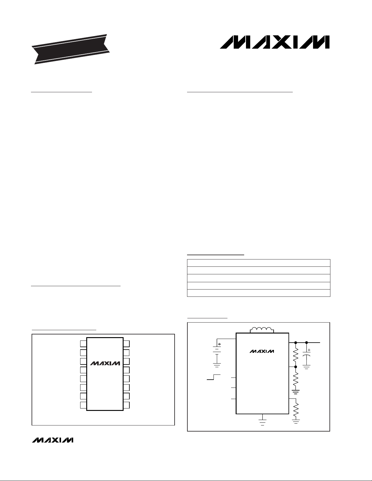
MAX1687
†
/MAX1688
†
Step-Up DC-DC Converters with
Precise, Adaptive Current Limit for GSM
________________________________________________________________
Maxim Integrated Products
1
16
15
14
13
12
11
10
9
1
2
3
4
5
6
7
8
IN OUT
OUT
LX2
LX2
PGND
PGND
AGND
ON
TOP VIEW
MAX1687
MAX1688
TSSOP
IN
LX1
FB
LX1
LIM [CHG]
REF
N.C.
[ ] ARE FOR MAX1688
Typical Operating Circuit
19-1426; Rev 0; 2/99
PART*
MAX1687EUE
MAX1687ESA
MAX1688EUE
-40°C to +85°C
-40°C to +85°C
-40°C to +85°C
TEMP. RANGE PIN-PACKAGE
16 TSSOP
8 SO
16 TSSOP
Pin Configurations
Ordering Information
MAX1688ESA -40°C to +85°C
8 SO
Pin Configurations continued at end of data sheet.
†
Patent pending
*
U.S. and foreign patents pending.
EVALUATION KIT MANUAL
FOLLOWS DATA SHEET
2.7V TO 6V
1 Li-lon
OR
3 NiMH
OR
3 ALKALINE
ON
OFF
0 TO 1V
CONTROL INPUT
( ) ARE FOR MAX1687
[ ] ARE FOR MAX1688
LX1 LX2
IN
MAX1687
MAX1688
ON
(LIM)
REF
GND
OUT
FB
[CHG]
V
OUT
UP TO 6V
Page 2
MAX1687/MAX1688
Step-Up DC-DC Converters with
Precise, Adaptive Current Limit for GSM
2 _______________________________________________________________________________________
ABSOLUTE MAXIMUM RATINGS
ELECTRICAL CHARACTERISTICS
(VIN= VON= +3V, V
LIM
= 1V (MAX1687), V
CHG
= 1V (MAX1688), VFB= 1.5V, V
OUT
= 6V, TA = 0°C to +85°C, unless otherwise noted.
Typical values are at T
A
= +25°C.)
Stresses beyond those listed under “Absolute Maximum Ratings” may cause permanent damage to the device. These are stress ratings only, and functional
operation of the device at these or any other conditions beyond those indicated in the operational sections of the specifications is not implied. Exposure to
absolute maximum rating conditions for extended periods may affect device reliability.
IN, ON, LX1, CHG, LIM, FB, OUT, REF to GND.......-0.3V to +7V
LX2 to GND ..............................................................-0.3V to +8V
IN, LX1 Average Current..........................................................1A
Continuous Power Dissipation (TA= +70°C)
TSSOP (derate 5.7mW/°C above +70°C) ....................457mW
SO (derate 5.88mW/°C above +70°C).........................471mW
Operating Temperature Range ...........................-40°C to +85°C
Storage Temperature Range .............................-65°C to +150°C
Lead Temperature (soldering, 10sec)............................+300° C
IN rising, 1% hysteresis
VFB= 0, V
OUT
= 3V (MAX1688)
VFB= 1.125V, V
OUT
= 3V (MAX1688)
VFBrising, 2% hysteresis
I
REF
= 0 to 10µA
VFB= 1.5V
Shutdown, VIN= 4.2V, LX2 connected to LX1,
V
OUT
= 0, ON = GND
V
LIM
= V
CHG
= 1V
CONDITIONS
0.744 0.8 0.856
Peak Current
VV
REF
6Output Voltage Range
V
2.4 2.5 2.6
V2.7 6Input Voltage Range
Input Undervoltage Lockout
µA60 110I
CHG
Source Current
mmho0.18 0.2 0.22g
mFB
FB Transconductance
V1.212 1.250 1.288FB Set Voltage
V1.225 1.25 1.275V
REF
Reference Voltage
mA
24
Input Supply Current
µA310
UNITSMIN TYP MAXSYMBOLPARAMETER
V
LIM
= V
CHG
= 1V
V
LIM
= V
CHG
= 0.65V
VIN= 2.7V
V
LIM
= 1V
VON= 0 or 3V
VIN= 2.7V
VIN= 6V
VIN= 4.2V
VFB= 1.5V
VIN= 2.7V Ω0.3 0.7P-Channel On-Resistance
Ω0.1 0.18R
SENSE
Sense Resistor
mA170 200 230I
RIPPLE
A
0.46 0.5 0.54
I
PEAK
Ripple Current
Ω0.4 0.8N-Channel On-Resistance
2
0.02 0.1
I
LIM
0.02 0.1I
ON
V0.6V
IL
V
1.8
ON Input Low Voltage
1.5
0.05 0.2I
FB
Input Current
VIN= V
LX2
= 6V, V
OUT
= VON= 0
VIN= 4V, V
FB
= 0, V
OUT
= 0
µA0.05 10
Ω30 70Precharge On-Resistance
LX2 Leakage Current
ms0.7 1.2 1.8t
DELAY
Shutdown Delay
V
IH
ON Input High Voltage
µA
TA= 0°C to +85°C
TA= +25°C
Page 3
MAX1687/MAX1688
Step-Up DC-DC Converters with
Precise, Adaptive Current Limit for GSM
_______________________________________________________________________________________ 3
ELECTRICAL CHARACTERISTICS
(VIN= VON= +3V, V
LIM
= 1V (MAX1687), V
CHG
= 1V (MAX1688), VFB= 1.5V, V
OUT
= 6V, TA= -40°C to +85°C, unless otherwise noted.)
(Note 1)
Note 1: Specifications to -40°C are guaranteed by design, not production tested.
V
LIM
= V
CHG
= 1V
V
LIM
= V
CHG
= 0.65V
I
IN
IN rising, 1% hysteresis
VFB= 1.125V, V
OUT
= 3V (MAX1688)
FB rising, 2% hysteresis
I
REF
= 0 to 10µA
VFB= 1.5V
Shutdown VIN= 4.2V, LX2 connected to LX1,
V
OUT
= 0, ON = GND
V
LIM
= V
CHG
= 1V
CONDITIONS
mA
145 240
I
RIPPLE
Ripple Current
A
0.44 0.57
I
PEAK
Ω
0.18
R
SENSE
Sense Resistor
0.73 0.90
Peak Current
V
2.35 2.65
V
2.7 6
Input Voltage Range
Input Undervoltage Lockout
mmho
0.16 0.24
gm
FB
FB Transconductance
V
1.20 1.30
FB Set Voltage
V1.212 1.288V
REF
Reference Voltage
ms
0.6 2
T
DELAY
Shutdown Delay
mA
5
I
SHDN
Input Supply Current
µA10
UNITSMIN TYP MAXSYMBOLPARAMETER
VIN= 4V, V
FB
= 0, V
OUT
= 0
VIN= 2.7V
VIN= 2.7V
Ω
70
Precharge On-Resistance
Ω
0.7
Ω
0.8
N-Channel On-Resistance
P-Channel On-Resistance
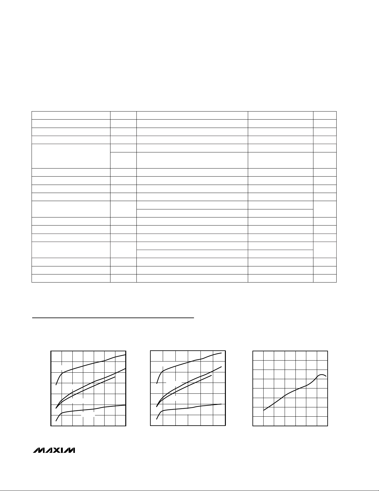
Typical Operating Characteristics
(VIN= +3.3V, V
OUT
= 5V, V
LIM
= 1V, Figures 6b and 7, TA= +25°C, unless otherwise noted.)
60
70
65
80
75
85
95
90
0 150 20050 100 250 300 350
EFFICIENCY vs. DC LOAD CURRENT
(V
OUT
= 5.5V)
MAX1687/88 toc01
LOAD CURRENT (mA)
EFFICIENCY (%)
VIN = 5V
VIN = 3.3V
VIN = 2.7V
VIN = 6V
60
65
70
75
80
85
90
95
0 1500500 1000 2000 2500 3000
EFFICIENCY vs. GSM BURST LOAD
(V
OUT
= 5.5V)
MAX1687/88 toc02
LOAD CURRENT (mA)
EFFICIENCY (%)
VIN = 5V
VIN = 3.3V
VIN = 2.7V
VIN = 6V
60
70
65
80
75
95
90
85
100
0 10050 150 200 250 300 350
EFFICIENCY vs. LOAD CURRENT
(V
IN
= 2.7V, V
OUT
= 3.3V)
MAX1687/88 toc03
LOAD CURRENT (mA)
EFFICIENCY (%)
VIN= 2.7V V
0.6
V
IL
ON Input Low Voltage
V
VIN= 6V
VIN= 4.2V
V
IH
ON Input High Voltage
1.8
1.5
V
V
REF
6
Output Voltage Range
Page 4
MAX1687/MAX1688
Step-Up DC-DC Converters with Precise,
Adaptive Current Limit for GSM
4 _______________________________________________________________________________________
_____________________________
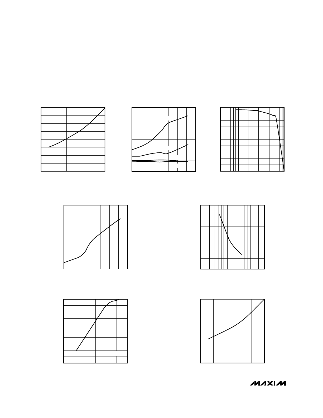
Typical Operating Characteristics (continued)
(V
IN
= +3.3V, V
OUT
= 5V, V
LIM
= 1V, Figures 6b and 7, TA= +25°C, unless otherwise noted.)
300
450
400
350
500
550
600
650
700
750
800
100 200150 250 300 350 400
MAX1688
I
PEAK
vs. V
OUT
DROOP
MAX1687/88 toc09
V
OUT
DROOP (mV)
I
PEAK
(mA)
R
CHG
= 40.2k
0
800
700
600
500
400
300
200
100
15 20 25 30 35 40
MAX1688 PEAK INDUCTOR CURRENT
vs. R
CHG
(1A GSM LOAD)
MAX1687/88 toc10
R
CHG
(kΩ)
PEAK INDUCTOR CURRENT (mA)
0
100
200
300
400
500
600
700
800
15 20 25 30 35 40
MAX1688 PEAK BATTERY CURRENT
vs. R
CHG
(1A GSM LOAD)
MAX1687/88 toc04
R
CHG
(kΩ)
PEAK BATTERY CURRENT (mA)
1.5
2.5
2.0
3.5
3.0
4.0
4.5
-40 20 40-20 0 60 80 100
TEMPERATURE (°C)
SUPPLY CURRENT (mA)
NO-LOAD BATTERY INPUT CURRENT vs.
TEMPERATURE (V
OUT
= 5V, V
LIM
= 1V )
MAX1687/88 toc05
VIN = 5V
VIN = 3.3V
VIN = 2.7V
VIN = 6V
REFERENCE VOLTAGE vs. REFERENCE
CURRENT (V
IN
= 3.3V, V
OUT
= 5V)
MAX1687/88 toc06
I
REF
(µA)
V
REF
(V)
1.245
1.200
1 100010010
1.215
1.205
1.235
1.225
1.250
1.220
1.210
1.240
1.230
1.245
1.247
1.249
1.251
1.253
TEMPERATURE (°C)
REFERENCE VOLTAGE (V)
-40 20 40-20 0 60 80 100
REFERENCE VOLTAGE vs. TEMPERATURE
(V
IN
= 3.3V, V
OUT
= 5V)
MAX1687/88 toc07
1200
0
1 10 100
SWITCHING FREQUENCY vs. INDUCTANCE
(V
IN
= 3.3V, V
OUT
= 5V,
I
LOAD
= 100mA, V
LIM
= 1V)
200
MAX1687/88 toc08
INDUCTANCE (µH)
FREQUENCY (kHz)
600
400
1000
800
Page 5

MAX1687/MAX1688
Step-Up DC-DC Converters with
Precise, Adaptive Current Limit for GSM
_______________________________________________________________________________________
5
Typical Operating Characteristics (continued)
(V
IN
= +3.3V, V
OUT
= 5V, V
LIM
= 1V, Figures 6b and 7, TA= +25°C, unless otherwise noted.)
500mA/div
500mA/div
200mV/div
V
OUT
1ms/div
I
LX
I
LOAD
MAX1688
SWITCHING WAVEFORMS
(GSM PULSED LOAD 1A, R
CHG
= 40.2kΩ)
MAX1687/88 toc11
R
CHL
= 40.2kΩ, L = 10µH
200mA/div
0A
V
LIM = 1V
V
LIM
= 0
2µs/div
I
LX
I
LX
INDUCTOR CURRENT
MAX1687/88 toc13
200mA/div
1V/div
I
BATTERY
V
ON
10µs/div
MAX1687/88 toc15
VON vs. BATTERY CURRENT
2V/div
1V/div
V
ON
V
OUT
5ms/div
MAX1687/88 toc14
POWER-UP WAVEFORM
(R
LOAD
= 15Ω C
OUT
= 2000µF)
500mA/div
500mA/div
200mV/div
V
OUT
1ms/div
I
LX
I
LOAD
MAX1688
SWITCHING WAVEFORMS
(GSM PULSED LOAD 1A, R
CHG
= 18kΩ)
MAX1687/88 toc12
R
CHG
= 18kΩ, L = 10µH
500mA/div
100mV/div
V
OUT
500µs/div
I
LX
SWITCHING WAVEFORMS
(FIXED I
LOAD
= 300mA)
MAX1687/88 toc10a
Page 6

MAX1687/MAX1688
Detailed Description
The MAX1687 and MAX1688 ICs supply power amplifiers in GSM applications where limited input current
surge is desirable. For example, GSM systems require
high-power, 12% duty-cycle RF bursts. Synchronizing
the MAX1687/MAX1688 to enter standby mode during
these RF bursts eliminates battery surge current and
minimizes switching noise to the power amplifier. In
standby mode, the charged output reservoir capacitor
delivers power to the power amplifier. Between each
burst, the DC-DC converter switches on to charge the
output capacitor. To improve efficiency and reduce peak
battery current, the MAX1687/MAX1688 provide a volt-
age-controlled current limit. The MAX1688 is a MAX1687
with added self-regulating circuitry that recharges the
reservoir capacitor in a fixed time (Figure 1).
Start-Up Sequence
In a conventional DC-DC converter, when high current
is required by the load, the battery voltage droops due
to battery series resistance. This may cause other circuitry that depends on the battery to malfunction or be
reset. The MAX1687/MAX1688 prevent battery voltage
droop by charging the reservoir capacitor during system off-time and isolate the battery from the output during high current demand. The MAX1687/MAX1688 are
gentle to the battery during initial power-up, as well.
Step-Up DC-DC Converters with
Precise, Adaptive Current Limit for GSM
6 _______________________________________________________________________________________
Pin Description
PIN
NAME FUNCTION
MAX1688MAX1687
—
10
11, 12
13, 14
15, 16
6
7
8
9
5
—
3, 4
1, 2
TSSOP
GND
AGND
PGND
LX2
OUT
FB
REF
N.C.
ON
CHG
LIM
LX1
IN
Ground
Analog Ground
Power Ground
N-Channel and P-Channel MOSFET Drain
Output
Feedback Input. Connect a resistor-divider from OUT to GND to
set the output voltage. FB regulates to a nominal 1.25V.
Reference Voltage Output. 1.25V nominal.
No Connection. Not internally connected.
Logic ON/OFF Input. When ON is high, the device operates in
normal mode. When ON goes low, the device goes into standby
mode. If ON remains low for greater than 1.2ms, the device shuts
down (see
Standby/Shutdown
section). The supply current falls to
3µA in shutdown mode.
Constant-Recharge-Time Input. Set the recharge time of the output reservoir capacitor by connecting a resistor from CHG to GND
(see
Applications Information
section).
Voltage-Controlled Current-Limit Adjust Input. Apply a voltage
between 0 and 1V to vary the current limit. LIM is internally
clamped to 1.25V.
Internal Current-Sense Resistor Output. Connect the inductor
between LX1 and LX2.
Supply Voltage Input. Connect Battery to IN. Bypass to GND with
a 47µF minimum capacitor.
6—6
—10—
—11, 12—
713, 147
815, 168
464
—7—
—8—
595
3——
—53
SO
23, 42
11, 2
1
SOTSSOP
Page 7

MAX1687/MAX1688
Step-Up DC-DC Converters with
Precise, Adaptive Current Limit for GSM
_______________________________________________________________________________________ 7
When starting up, the MAX1687/MAX1688 employ four
successive phases of operation to reduce the inrush of
current from the battery. These phases are Linear
Regulator Mode, Pseudo Buck Mode, Pseudo Boost
Mode, and Boost Mode. In Linear Mode, the output
connects to the input through a 30Ω precharge PMOS
device (Figure1, Q1). The transition from Linear Mode
to Pseudo Buck Mode occurs when V
OUT
= VIN- 3V.
The transition from Pseudo Buck Mode to Pseudo
Boost Mode occurs when V
OUT
= VIN- 0.7V. The transition from Pseudo Boost Mode to Boost Mode occurs
when V
OUT
> VIN. Due to these mode changes, the
battery input current remains relatively constant, and
V
OUT
changes slope as it rises.
Hysteretic Inductor-Current Control
Logic circuits in the MAX1687/MAX1688 control the
inductor ripple current to typically 200mA (Figure 2).
The voltage at LIM (CHG) programs I
PEAK
. The induc-
tor current oscillates between I
PEAK
- 200mA and
I
PEAK
.
Standby/Shutdown
When ON goes low, the device enters Standby Mode,
inductor current ramps to zero, and the output disconnects from the input. If ON remains low for greater than
1.2ms (typ), the device shuts down and quiescent current drops to 3µA (typ).
Q3
REF
FB
V
OUT
V
OUT
V
PRECHARGE
V
IN
g
m
ON
( ) ARE FOR MAX1687
[ ] ARE FOR MAX1688 (ALSO DASHED LINES)
(LIM)
[CHG]
g
m
VIN - V
DIODE
CONSTANT
HYSTERETIC
INDUCTOR-CURRENT
CONTROL LOGIC
PEAK/
TROUGH
INDUCTOR-
CURRENT
DETECT
Q2
P-SWITCH
N-SWITCH
ZERO
CROSSING
P-SWITCH
LX2
Q1
LX1
V
IN
MAX1687
MAX1688
TIMER
Figure 1. Functional Diagram
Page 8

MAX1687/MAX1688
Step-Up DC-DC Converters with
Precise, Adaptive Current Limit for GSM
8 _______________________________________________________________________________________
Synchronized ON Pin
If desired, drive ON low during periods of high current
demand to eliminate switching noise from affecting
sensitive RF circuitry. During the periods when ON is
low, the output reservoir capacitor provides current to
the load (Figure 4).
Buck Capability
Although the IC is not intended for this application, the
MAX1687/MAX1688 operate as a buck converter when
the input voltage is higher than the output voltage. The
MAX1687/MAX1688 are not optimally efficient in this
mode (see
Typical Operating Characteristics
for
efficiencies at 2.7V, 3.3V, 5V, and 6V input supply voltages).
Applications Information
Adjusting the Output Voltage
Adjust the MAX1687/MAX1688 output voltage with two
external resistors (Figure 3). Choose R2 to be between
10kΩ to 100kΩ. Calculate R1 as follows:
R1 = R2 · (V
OUT
- VFB) / V
FB
where VFBis the feedback threshold voltage, 1.25V
nominal.
Adjusting Current Limit (MAX1687)
The MAX1687 has an adjustable current limit for applications requiring limited supply current, such as PC
card sockets or applications with variable burst loads.
For single Li-Ion battery cell applications, the high peak
current demands of the RF transmitter power amplifier
can pull the battery very low as the battery impedance
increases toward the end of discharge. The reservoir
capacitor at the output supplies power during load-current bursts; this allows for a lower input current limit.
With this feature, the life of the Li-Ion battery versus the
reservoir capacitor size trade-off can be optimized for
each application.
( ) ARE FOR MAX1688
I
PEAK
- 200mA
I
PEAK
SET BY
V
LIM (VCHG
)
HYSTERESIS
BAND
CURRENT
TIME
Figure 2. Hysteretic Inductor Current
OUT
V
OUT
R1
R2
R1 = R2
V
OUT
- V
FB
V
FB
FB
( )
MAX1687
MAX1688
Figure 3. Setting the Output Voltage
“ON”
CONTROL INPUT
V
OUT
I
LOAD
TIME
Figure 4. Timing Diagram of “ON”
Page 9

MAX1687/MAX1688
Step-Up DC-DC Converters with
Precise, Adaptive Current Limit for GSM
_______________________________________________________________________________________ 9
To set the current limit, apply a voltage of 0 to 1V at
LIM. The current limit is 200mA when V
LIM
= 0 to
0.25V. Use the following equation to calculate I
LIM
:
I
LIM
= V
LIM
(0.86A/V) – 0.06A
where V
LIM
= 0.25V to 1V.
V
LIM
is internally clamped to 1.25V when the voltage
applied at V
LIM
is above 1.25V. Generate V
LIM
by one
of three methods: an externally applied voltage, the
output of a DAC, or a resistor-divider using V
REF
as the
supply voltage (TSSOP packages) (Figure 5). Note that
REF can supply up to 10µA.
Determine V
LIM
as follows:
V
LIM
= (I
LX(PEAK)
+ 0.06A) / 0.86
where I
LX(PEAK)
= [(I
LOAD
· V
OUT
) / VIN] + 0.1A (see
the Inductor Current parameter in the
Typical Operating
Characteristics
).
Setting Recharge Time (MAX1688)
The MAX1688 has a recharging feature employing a
sample-and-hold, which sets the maximum time to
recharge the reservoir capacitor. Synchronize the ON
pin to place the converter in standby during each load
current burst. At the end of each load current burst, the
output voltage is sampled by the MAX1688. This voltage controls the peak inductor current. The greater the
difference between the regulated output voltage and
the valley of the sag voltage, the higher the peak current. This results in a constant recharge time that compensates for varying output filter capacitor characteristics as well as a varying input voltage. Therefore, the
circuit demands only as much peak current from the
battery as output conditions require, minimizing the
peak current from the battery. An external resistor
between CHG and GND controls the output recharge
time. A large resistor increases peak inductor current
which speeds up recovery time. Calculate the resistor
as follows:
where:
R
CHG
is the external resistor
I
BURST
is the peak burst current expected
D
GSM
is the duty cycle of GSM
VINis the input voltage
V
OUT
is the output voltage
V
REF
= 1.25V
V
DROOP
is the drop in output voltage during the cur-
rent burst
g
mCHG
is the internal transconductance = 0.8A/V
g
mFB
is the feedback transconductance = 200µA/V
tol is the tolerance of the R
CHG
resistor
For example, for I
BURST
= 2.66A, V
DROOP
= 0.36V, V
IN
= +2.7V, and V
OUT
= 3.6V, then R
CHG
= 31.5kΩ, using
a 5% tolerance resistor.
The recovery time for a 40.2kΩ R
CHG
is shorter than
that with an 18kΩ R
CHG
, but the peak battery current is
higher. See Switching Waveforms (GSM Pulsed Load
1A, R
CHG
= 40.2kΩ) and Switching Waveforms (GSM
Pulsed Load 1A, RCH= 18kΩ) in
Typical Operating
Characteristics
.
Inductor Selection
The value of the inductor determines the switching frequency. Calculate the switching frequency as:
f = VIN[1 - (VIN/ V
OUT
)] / (L · I
RIPPLE
)
where f is the switching frequency, VINis the input voltage, V
OUT
is the output voltage, L is the inductor value,
and I
RIPPLE
is the ripple current expected, typically
0.2A. Using a lower value inductor increases the frequency and reduces the physical size of the inductor.
A typical frequency is from 150kHz to 1MHz (see
Switching Frequency vs. Inductance in the
Typical
Operating Characteristics
).
DAC REF
REF
a)
c)
b)
LIM
LIM
V
LIM(CHG)
= V
REF
R3
+
R4 > 125kΩ
R4
R4 + R3
R3
R4
LIM
MAX1687
MAX1687 MAX1687
Figure 5. Current-Limit Adjust
R =
I V D
V 1 - D
+ 0.1
V
V gm V gm 1 - tol
CHG
BURST OUT GSM
IN(MIN) GSM
IN(MIN)
DROOP CHG REF FB
⋅⋅
⋅
⋅
⋅⋅⋅⋅
()
()
()
Page 10

MAX1687/MAX1688
Step-Up DC-DC Converters with
Precise, Adaptive Current Limit for GSM
10 ______________________________________________________________________________________
Output (Reservoir) Capacitor
The value of the output capacitor determines the
amount of power available to deliver to the power
amplifier during the RF burst. A larger output capacitor
with low ESR reduces the amount of output voltage
droop during an RF burst. Use the following equation to
determine capacitor size when ON is synchronized to
the RF burst:
where C
OUT
is the output capacitor, I
BURST
is the peak
power amplifier burst current, t
GSM
is the current pulse
period, D
GSM
is the duty cycle, tol is the capacitor tol-
erance, and V
DROOP
is the acceptable drop in the out-
put during the current burst.
For example, when used in a typical GSM system,
t
GSM
= 4.62ms, I
BURST
= 2.66A for a +3.6V system
(1.42A for a +5.5V system), and with a droop of less
than 10%, the value of the capacitor is 5.3mF ±20%.
The output capacitor also determines the constant-load
(ON connected to VCC) ripple voltage. The output ripple is:
V
RIPPLE
= I
RIPPLE
· ESR
(OUTPUT CAPACITOR)
where I
RIPPLE
is typically 0.2A.
Typical Application Circuits
The current limit of the MAX1687 can be set by an external DAC (Figure 6a), making it variable by using a microcontroller. The MAX1687 is the choice for systems
interfacing with a microcontroller, but may also be used
with fixed current limit (Figure 6b). The MAX1688 can
monitor the droop of the output voltage to set the current
limit, maximizing battery life. The MAX1688 is suitable for
systems demanding variable burst currents (Figures 6a,
6b, and 7) as well as variable input voltages.
Layout
The MAX1687/MAX1688’s high-frequency operation
and high peak currents make PC board layout critical
to minimize ground bounce and noise. Locate input
bypass and output filter capacitors as close to the
device pins as possible. All connections to OUT and FB
should also be kept as short as possible. Use a lowinductance ground plane. Connect the ground leads of
the input capacitor, output capacitor, and PGND pins in
a star configuration to the ground plane. Table 1 lists
suggested suppliers. Refer to the MAX1687/MAX1688
evaluation kit manual for a suggested surface-mount
layout and a list of suggested components.
C =
D I t
V - I ESR 1 - tol
OUT
GSM BURST GSM
DROOP BURST OUTPUT CAPACITOR
⋅⋅
⋅
()()
V
OUT
= 5V
2A AT 12%
DUTY CYCLE
OUT
OUT
IN
IN
0.1µF
47µF
V
IN
2.7V TO 6V
10µH
2000µF
R2
187k
R1
61.9k
LX1
LX1
LX2
LX2
ON
ON
OFF
DAC
OUTPUT
0 TO 1V
LIM
REF
FB
AGND
PGND
PGND
MAX1687
Figure 6a. MAX1687 Typical Application Circuit (GSM Pulsed Load)
Page 11

MAX1687/MAX1688
Step-Up DC-DC Converters with
Precise, Adaptive Current Limit for GSM
______________________________________________________________________________________________________ 11
OUT
OUT
IN
IN
0.1µF
47µF
V
IN
2.7V TO 6V
R
CHG
40.2k
10µH
2000µF
R2
187k
R1
61.9k
LX1
LX1
LX2
LX2
ON
ON
OFF
REF
CHG
FB
AGND
PGND
PGND
V
OUT =
5V
2A AT 12%
DUTY CYCLE
MAX1688
Figure 7. MAX1688 Typical Application Circuit (GSM Pulsed Load)
V
OUT =
5V
350mA
OUT
OUT
IN
IN
0.1µF
47µF
V
IN
2.7V TO 6V
10µH
47µF
R2
187k
R1
61.9k
LX1
LX1
LX2
LX2
ON
ON
OFF
LIM
REF*
FB
AGND
PGND
PGND
*TSSOP PACKAGE ONLY
MAX1687
Figure 6b. MAX1687 Typical Application Circuit (Fixed Non-Pulsed Load)
Page 12

MAX1687/MAX1688
Step-Up DC-DC Converters with
Precise, Adaptive Current Limit for GSM
12 ______________________________________________________________________________________
Package Information
Table 1. Component Suppliers
COMPANY FAX PHONE
AVX 207-283-1941 207-282-5111
CoilCraft 708-639-6400 708-639-1469
Coiltronics 561-241-9339 561-241-7876
Murata-Erie 404-736-3030 404-736-1300
Sumida 81-3-3607-5428 708-956-0666
Chip Information
TRANSISTOR COUNT: 1920
Pin Configurations (continued)
GND
ONFB
1
2
87OUT
LX2LX1
LIM [CHG]
IN
SO
TOP VIEW
[ ] ARE FOR MAX1688
3
4
6
5
MAX1687
MAX1688
TSSOP.EPS
 Loading...