

Page 1
For free samples & the latest literature: http://www.maxim-ic.com, or phone 1-800-998-8800.
For small orders, phone 1-800-835-8769.
General Description
The MAX1686 provides power for dual-voltage subscriber ID module (SIM) cards in portable applications
such as GSM cellular phones. Designed to reside in the
portable unit (cellular phone handset), the 1MHz charge
pump converts a 2.7V to 4.2V input to regulated 5V output. The MAX1686H has a nominal output voltage of
5.0V, while the MAX1686 is set to 4.75V to reduce SIMcard current drain. The charge pump has only 45µA quiescent supply current, which reduces to 3µA when a
3V-capable SIM card is being powered and the charge
pump is disabled. An internal input/output shorting
switch provides power for 3V SIM cards.
The MAX1686/MAX1686H require only three external
capacitors around their space-saving, thin (1mm) 8-pin
µMAX packages.
Applications
GSM Cellular Phones
PCS Phones
Portable POS Terminals
Personal Communicators
Features
♦ 2.7V to 4.2V Input Range
♦ 12mA min Charge-Pump Output Current
♦ 45µA Quiescent Supply Current
♦ 0.1µA Supply Current in Shutdown Mode
♦ 5.0V Regulated Charge-Pump Output (MAX1686H)
4.75V Regulated Charge-Pump Output (MAX1686)
♦ Input-Output Shorting Switch for 3V Cards
♦ Small External Components
(Uses a 0.047µF, 0.1µF, and a 2.2µF Capacitor)
♦ Output Driven to Ground in Shutdown Mode
♦ Super-Small 8-Pin µMAX Package
♦ Soft-Start and Short-Circuit Protection
MAX1686/MAX1686H
3V to 5V Regulating
Charge Pumps for SIM Cards
________________________________________________________________
Maxim Integrated Products
1
1
2
3
4
8
7
6
5
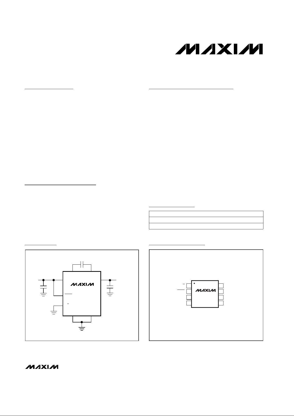
OUT
CXP
CXN
PGNDGND
IN
SHDN
3/5
MAX1686
MAX1686H
µMAX
TOP VIEW
MAX1686
MAX1686H
IN
CXN CXP
GND PGND
C
IN
INPUT
2.7V TO 4.2V
OUTPUT
V
IN
OR 5V/20mA
C
X
C
OUT
SHDN
3/5
OUT
Typical Operating Circuit
19-1376; Rev 1; 12/98
PART
MAX1686EUA
-40°C to +85°C
TEMP. RANGE PIN-PACKAGE
8 µMAX
Pin Configuration
Ordering Information
MAX1686HEUA
-40°C to +85°C 8 µMAX
Page 2
MAX1686/MAX1686H
3V to 5V Regulating
Charge Pumps for SIM Cards
2 _______________________________________________________________________________________
ABSOLUTE MAXIMUM RATINGS
ELECTRICAL CHARACTERISTICS
(VIN= V
SHDN
= 3.3V, 3/5 = GND, CX= 0.22µF, C
OUT
= 10µF (see
Applications Information
section to use smaller capacitors),
T
A
= T
MIN
to T
MAX
, unless otherwise noted. Typical values are at TA= +25°C.) (Note 1)
IN, OUT, SHDN, 3/5 to GND.....................................-0.3V to +6V
CXP to GND..............................................-0.3V to (V
OUT
+ 0.3V)
CXN to GND ................................................-0.3V to (V
IN
+ 0.3V)
PGND to GND ......................................................-0.3V to + 0.3V
OUT Short Circuit to GND..........................................Continuous
IN-to-OUT Current...............................................................50mA
Continuous Power Dissipation (T
A
= +70°C )
8-Pin µMAX (derate 4.1mW/°C above +70°C).............330mW
Operating Temperature Range
MAX1686EUA/MAX1686HEUA........................-40°C to +85°C
Junction Temperature......................................................+150°C
Storage Temperature Range.............................-65°C to +165°C
Lead Temperature (soldering, 10sec).............................+300°C
PARAMETER
CONDITIONS MIN TYP MAX UNITS
Input Voltage Range 2.7 4.2 V
Input Undervoltage-Lockout
Threshold Voltage
0.8 1.2 1.6 V
Quiescent Supply Current
Charge pump enabled,
no load, 3/5 = GND
µA
Charge pump disabled, no load, 3/5 = IN
Shutdown Supply Current
V
IN
= 3.6V, SHDN = GND
0.1 5
VOUT Output Voltage
4.55 4.75 5.25
V
3/5
= VIN= 3.0V 2.5 5 Ω
OUT Short-Circuit Current
3/5 = GND or IN
20 100 200 mA
Logic Input Low Voltage
SHDN, 3/5
0.5 · VIN0.3 · V
IN
V
Logic Input High Voltage
SHDN, 3/5
0.7 · VIN0.5 · V
IN
V
Logic Input Leakage Current
SHDN, 3/5 = GND or IN
0.1 1 µA
4.75 5.00 5.25
OUT Discharge Switch On-Resistance
3/5 = GND or IN, SHDN = GND
80 200 Ω
IN-to-OUT Switch On-Resistance
TA= +25°C 800 1000 1200
µA
Note 1: Electrical specifications are measured by pulse testing and are guaranteed for a junction temperature within the operating
temperature range, unless otherwise noted. Limits are 100% production tested at T
A
= +25°C. Limits over the entire operating temperature range are guaranteed through correlation using Statistical Quality Control (SQC) methods and are not production tested.
Stresses beyond those listed under “Absolute Maximum Ratings” may cause permanent damage to the device. These are stress ratings only, and functional
operation of the device at these or any other conditions beyond those indicated in the operational sections of the specifications is not implied. Exposure to
absolute maximum rating conditions for extended periods may affect device reliability.
TA= +25°C 45 100
310
Charge-Pump Frequency
TA= -40°C to +85°C 700 1300
kHz
TA= -40°C to +85°C 150
3/5 = IN
V
IN
MAX1686
MAX1686H
VIN= 2.7V to 4.2V,
load = 0 to 12mA
Page 3
MAX1686/MAX1686H
3V to 5V Regulating
Charge Pumps for SIM Cards
_______________________________________________________________________________________
3
0
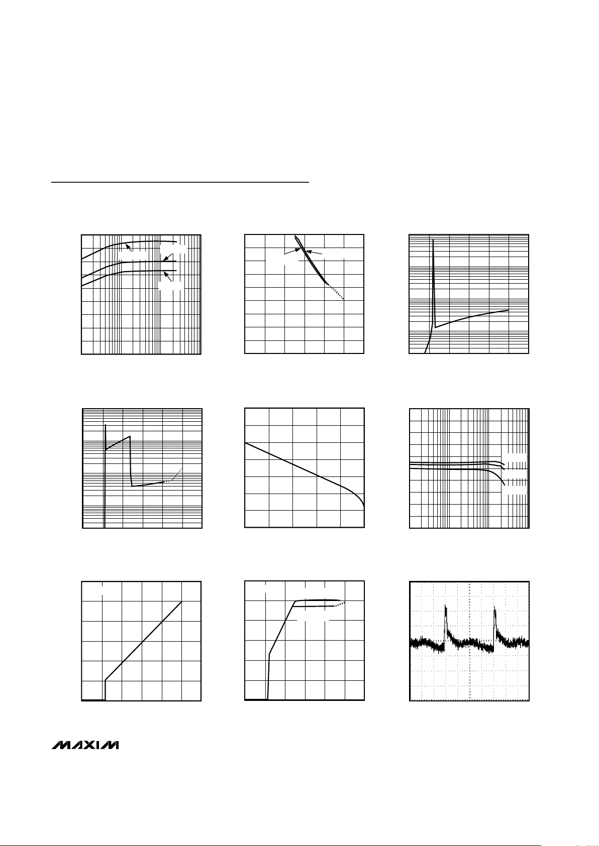
0.1 100101
EFFICIENCY vs. LOAD CURRENT
(5V MODE)
30
10
70
50
90
40
20
80
60
MAX1686-01
LOAD CURRENT (mA)
EFFICIENCY (%)
V
IN
= 3.6V
V
IN
= 2 .7V
V
IN
= 3.3V
0
0
EFFICIENCY vs. INPUT VOLTAGE
(5V MODE)
MAX1686-TOC2
INPUT VOLTAGE (V)
EFFICIENCY (%)
10
20
30
40
50
60
70
80
90
123 456
I
LOAD
= 10mA
I
LOAD
= 1mA
1000
0.1
02146
NO-LOAD INPUT CURRENT
vs. INPUT VOLTAGE (3V MODE)
1
10
100
MAX1686-03
INPUT VOLTAGE (V)
INPUT CURRENT (µA)
35
10,000
1
02146
NO-LOAD INPUT CURRENT
vs. INPUT VOLTAGE (5V MODE)
10
100
1000
MAX1686-04
INPUT VOLTAGE (V)
INPUT CURRENT (µA)
35
0
2
1
4
3
5
6
0231 456
OUTPUT VOLTAGE
vs. INPUT VOLTAGE (3V MODE)
MAX1686-07
INPUT VOLTAGE (V)
OUTPUT VOLTAGE (V)
NO LOAD
3.20
3.24
3.22
3.28
3.26
3.30
3.34
3.32
0 5 10 15 20 25
OUTPUT VOLTAGE
vs. LOAD CURRENT (3V MODE)
MAX1686-05
LOAD CURRENT (mA)
OUTPUT VOLTAGE (V)
4.70
0.1 100101
MAX1686 OUTPUT VOLTAGE
vs. LOAD CURRENT (5V MODE)
4.73
4.71
4.77
4.75
4.80
4.74
4.72
4.78
4.79
4.76
MAX1686-06
LOAD CURRENT (mA)
OUTPUT VOLTAGE (V)
V
IN
= 2.7V
V
IN
= 3 .3V
V
IN
= 3.6V
0
2
1
4
3
5
6
0231 456
OUTPUT VOLTAGE
vs. INPUT VOLTAGE (5V MODE)
MAX1686-08
INPUT VOLTAGE (V)
OUTPUT VOLTAGE (V)
NO LOAD
MAX1686
MAX1686H
2.5µs/div
OUTPUT WAVEFORM
(I
LOAD
= 10mA)
MAX1686-09
V
OUT
(20mV/div)
5V MODE, AC COUPLED,
C
OUT
= 10µF 0.1µF
Typical Operating Characteristics
(See
Typical Operating Circuit
, CIN= 0.47µF, CX= 0.22µF, C
OUT
= 10µF, VIN= 3.3V, TA= +25°C, unless otherwise noted.)
Page 4

MAX1686/MAX1686H
3V to 5V Regulating
Charge Pumps for SIM Cards
4 _______________________________________________________________________________________
Typical Operating Characteristics (continued)
(See
Typical Operating Circuit
, CIN= 0.47µF, CX= 0.22µF, C
OUT
= 10µF, VIN= 3.3V, TA= +25°C, unless otherwise noted.)
25µs/div
OUTPUT WAVEFORM
(I
LOAD
= 1mA)
MAX1686-10
V
OUT
(20mV/div)
5V MODE, AC COUPLED,
C
OUT
= 10µF 0.1µF
2.5ms/div
LINE-TRANSIENT RESPONSE
MAX1686-11
V
IN
(500mV/div)
V
IN
= 2.8V to 3.3V, I
LOAD
= 10mA, 5V MODE,
AC COUPLED
V
OUT
(50mV/div)
2.5ms/div
LOAD-TRANSIENT RESPONSE
MAX1686-12
I
LOAD
(10mA/div)
I
LOAD
= 0 TO 10mA, 5V MODE, AC COUPLED
V
OUT
(50mV/div)
250µs/div
START-UP WAVEFORM
(3V MODE, R
L
= 500Ω)
MAX1686-13
SHDN
(5V/div)
V
OUT
(1V/div)
0V
1ms/div
SHUTDOWN WAVEFORM
(3V MODE, NO LOAD)
MAX1686-16
SHDN
(5V/div)
V
OUT
(1V/div)
RL = 500Ω
0V
250µs/div
START-UP WAVEFORM
(5V MODE, R
L
= 500Ω)
MAX1686-14
SHDN
(5V/div)
V
OUT
(1V/div)
0V
250µs/div
3V MODE TO 5V MODE
WAVEFORM (R
L
= 500Ω)
MAX1686-15
3/5
(5V/div)
V
OUT
(1V/div)
0V
1ms/div
SHUTDOWN WAVEFORM
(5V MODE, NO LOAD)
MAX1686-17
SHDN
(5V/div)
V
OUT
(1V/div)
0V
500µs/div
5V MODE TO 3V MODE
WAVEFORM (NO LOAD)
MAX1686-18
3/5
(5V/div)
V
OUT
(1V/div)
0V
Page 5

MAX1686/MAX1686H
3V to 5V Regulating
Charge Pumps for SIM Cards
_______________________________________________________________________________________ 5
NAME FUNCTION
1
3/5
3V/5V Select Input. When low, the output is regulated at 4.75V for MAX1686, 5.00V for MAX1686H. When
high, the output is shorted to the input.
2
SHDN Active-Low Shutdown Input. SHDN = GND is off. Output is actively pulled low in shutdown.
PIN
3 IN Supply Input Pin. Can range from 2.7V to 4.2V. Bypass to ground with a ceramic capacitor.
4 GND Ground Pin
8 OUT Power Output. Bypass to GND with an output filter capacitor.
7 CXP Positive Terminal of the Charge-Pump Transfer Capacitor
6 CXN Negative Terminal of the Charge-Pump Transfer Capacitor
5 PGND Power Ground. Connect to GND through a short trace.
Pin Description
_______________Detailed Description
The MAX1686/MAX1686H charge pumps provide two
modes of operation: 3V mode or 5V mode. The devices
consist of an error amplifier, a 1.23V bandgap reference, an internal resistive feedback network, a 1MHz
oscillator, high-current MOSFET drivers and switches,
and a power-management block as shown in the
Functional Diagram
(Figure 1). In 3V mode (3/5 = IN),
the input is connected to the output through a 2.5Ω
switch. In 5V mode (3/5 = GND), the MAX1686’s output
voltage is regulated at 4.75V (5.00V for the MAX1686H)
with a 2.7V to 4.2V input and can deliver more than
12mA of load current.
Designed specifically for compact applications, these
regulators require only three small external capacitors.
The Skip Mode control scheme provides high efficiency
over a wide output current range. The devices offer a
shutdown feature which actively discharges the output
to ground and reduces the supply current to less than
MAX1686
MAX1686H
C
X
POWER
MANAGEMENT
DIS
SS
OSC
CXPCXN
EN
SHDN
3/5
1.23V
GND
PGND
IN
S1
S2
PWROK
OUT
Figure 1. Functional Diagram
Page 6

MAX1686/MAX1686H
3V to 5V Regulating
Charge Pumps for SIM Cards
6 _______________________________________________________________________________________
1µA. Other features include soft-start, undervoltage
lockout, and short-circuit protection.
Charge-Pump Control
Figure 2 shows an idealized, unregulated charge-pump
voltage doubler. The oscillator runs at a 50% duty
cycle. During one half of the period, the transfer capacitor (CX) charges to the input voltage. During the other
half, the doubler stacks the voltage across CX and the
input voltage, and transfers the sum of the two voltages
to the output filter capacitor (C
OUT
). The MAX1686 uses
Skip Mode control to regulate its output voltage and to
achieve good efficiency over a large output current
range. When the comparator detects that the output
voltage is too low, the 1MHz oscillator is enabled and
CXis switched. When the output voltage is above regulation, the oscillator is disabled and CXis connected at
the input.
Soft-Start
In the 5V mode (3/5 = GND), the start-up current is limited by the soft-start control to typically 200mA, independent of the load. Until the output voltage reaches
V
IN
/ 2, the input is connected to the output through a
50Ω series P-channel MOSFET and the charge pump
is disabled. For V
IN
/ 2 < V
OUT
< 4.75V (5.00V for
MAX1686H) and for a maximum of 2ms the charge
pump is active, but R
ON
of the switch S2 is limited to
50Ω. This limits typical current surges associated with
charge pumps at start-up. When soft-start is complete,
V
OUT
> 4.75V (5.00V for MAX1686H) or 2ms (whichever
occurs first), switch S2’s on-resistance is decreased to
minimize losses.
In 3V mode (3/5 = IN), the start-up current is limited by
the 50Ω series P-channel MOSFET connected between
IN and OUT until the output voltage reaches V
IN
/ 2. For
V
OUT
> V
IN
/ 2, RONis reduced to 2.5Ω.
With a 500Ω load the device turns on in less than 1.5ms
(see
Typical Operating Characteristics
for graphs of
start-up waveforms).
Shutdown Mode
Driving SHDN low places the device in shutdown mode,
which disables the oscillator, the control logic, and the
reference. Placing the device in shutdown mode
reduces the no-load supply current to less than 1µA; the
output is actively discharged through the internal Nchannel FET and disconnected from the input. In normal
operation, SHDN is driven high or connected to IN.
Applications Information
Capacitor Selection
The MAX1686 requires only three external capacitors.
The capacitor values are closely linked to the output
current capability, noise, and switching frequency. The
1MHz oscillator frequency minimizes capacitor size
compared to lower-frequency charge pumps.
Generally, the transfer capacitor (CX) will be the
smallest, the input capacitor (CIN) will be twice the size
of CX, and the output capacitor (C
OUT
) can be from 10
to 50 times CX. The suggested capacitor values are
CIN= 0.1µF, CX= 0.047µF, and C
OUT
= 2.2µF as
shown in Figure 3. For input voltages as low as 2.7V,
the following values are recommended: CIN= 0.47µF,
CX= 0.22µF, and C
OUT
= 10µF. Table 1 lists the perfor-
C
X
OSC
CXPCXN
GND
IN
S1
S2
OUT
C
IN
C
OUT
Figure 2. Unregulated Voltage Doubler
MAX1686
IN
38
2
1
45
6
7
CXN CXP
GND PGND
C
IN
0.1µF
3V
5V
INPUT
2.85V TO 4.2V
OUTPUT
V
IN
OR 4.75V AT 20mA
C
X
0.047µF
C
OUT
2.2µF
(CERAMIC)
SHDN
3/5
OUT
Figure 3. Standard Application Circuit
Page 7

MAX1686/MAX1686H
3V to 5V Regulating
Charge Pumps for SIM Cards
_______________________________________________________________________________________ 7
mance with different input voltages and an additional
small 0.1µF capacitor at the output. The extra 0.1µF
capacitor improves start-up capability under full load
and reduces output ripple for high input voltages. Table
2 lists the recommended capacitor manufacturers.
Low-ESR capacitors, such as surface-mount ceramics,
decrease noise and give the best efficiency. Capacitance and ESR variation over temperature need to be
taken into consideration for best performance in applications with large operating temperature ranges.
For applications where the minimum input voltage is 3V
or greater, the flying capacitor, CX, can be decreased
to 0.1µF. This provides two benefits: the inrush surge
current at start-up is reduced, and the output ripple
voltage (especially at high input voltages) is also
reduced.
Layout Considerations
High switching frequencies and large peak currents
make PC board layout an important part of design. All
capacitors should be soldered close to the IC. Connect ground and power ground through a short, lowimpedance trace. Keep the extra copper on the board
and integrate it into ground as a pseudo-ground plane.
On multilayer boards, route the star ground using component-side copper fill, then connect it to the internal
ground plane using vias. Ensure that the load is connected directly across the output filter capacitor.
2.7 1 30 84.3
2.7 10 30 86.2
3.3 1 60 69.5
3.3 10 60 70.5
3.6 1 80 63.2
3.6 10 80 63.8
4.2 1 120 52.3
4.2 10 120 52.1
Table 2. Recommended Surface-Mount
Capacitor Manufacturers
VALUE
(µF)
DESCRIPTION MFR.
PHONE
NUMBER
1 to 47
595D-series
tantalum
Sprague (603) 224-1961
4.7 to 47
TPS-series
tantalum
AVX (803) 946-0690
1 to10
267 series
tantalum
Matsuo (714) 969-2491
0.047 to 2.2 X7R ceramic
TDK (847) 390-4373
AVX (803) 946-0690
INPUT
VOLTAGE
(V)
LOAD
CURRENT
(mA)
V
OUT
RIPPLE
(mV)
EFFICIENCY
(%)
Table 1. Ripple and Efficiency vs. Input
Voltage and Load Current
Chip Information
TRANSISTOR COUNT: 840
Page 8

MAX1686/MAX1686H
3V to 5V Regulating
Charge Pumps for SIM Cards
Maxim cannot assume responsibility for use of any circuitry other than circuitry entirely embodied in a Maxim product. No circuit patent licenses are
implied. Maxim reserves the right to change the circuitry and specifications without notice at any time.
8
_____________________Maxim Integrated Products, 120 San Gabriel Drive, Sunnyvale, CA 94086 408-737-7600
© 1998 Maxim Integrated Products Printed USA is a registered trademark of Maxim Integrated Products.
Package Information
8LUMAXD.EPS
 Loading...