

Page 1
For free samples & the latest literature: http://www.maxim-ic.com, or phone 1-800-998-8800.
For small orders, phone 408-737-7600 ext. 3468.
General Description
The MAX1678 is a high-efficiency, low-voltage, synchronous-rectified, step-up DC-DC converter intended
for use in devices powered by 1 to 3-cell alkaline,
NiMH, or NiCd batteries or a 1-cell lithium battery. It
guarantees a 0.87V start-up voltage and features a low
37µA quiescent supply current.
The device includes a 1Ω, N-channel MOSFET power
switch, a synchronous rectifier that acts as the catch
diode, a reference, pulse-frequency-modulation (PFM)
control circuitry, and circuitry to reduce inductor ringing—all in an ultra-small, 1.1mm-high µMAX package.
The output voltage is preset to 3.3V or can be adjusted
from +2V to +5.5V using only two resistors. Efficiencies
up to 90% are achieved for loads up to 50mA. The
device also features an independent undervoltage
comparator (PFI/PFO) and a logic-controlled 2µA shutdown mode.
Applications
Pagers
Remote Controls
Pointing Devices
Personal Medical Monitors
Single-Cell Battery-Powered Devices
Features
♦ 0.87V Guaranteed Start-Up
♦ Up to 90% Efficiency
♦ Built-In Synchronous Rectifier (no external diode)
♦ Ultra-Small µMAX Package, 1.1mm High
♦ 37µA Quiescent Current (85µA from 1.5V battery)
♦ 2µA Logic-Controlled Shutdown
♦ Power-Fail Detector
♦ Dual Mode™ Output: Fixed 3.3V
Adjustable 2V to 5.5V
♦ 45mA Output Current at 3.3V for 1-Cell Input
♦ 90mA Output Current at 3.3V for 2-Cell Input
♦ Inductor-Damping Switch Suppresses EMI
MAX1678
1-Cell to 2-Cell, Low-Noise,
High-Efficiency, Step-Up DC-DC Converter
________________________________________________________________
Maxim Integrated Products
1
1
2
3
4
8
7
6
5
OUT
LX
GND
FBSHDN
PFO
PFI
BATT
MAX1678
µMAX
TOP VIEW
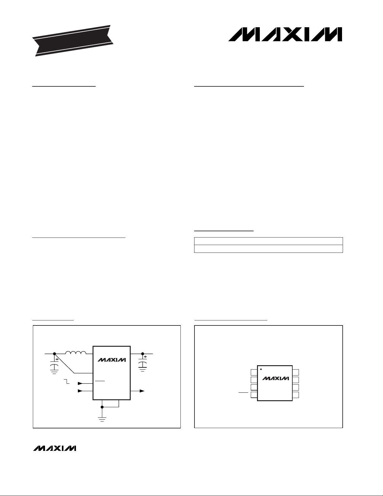
Typical Operating Circuit
19-1381; Rev 0; 7/98
PART
MAX1678EUA -40°C to +85°C
TEMP. RANGE PIN-PACKAGE
8 µMAX
EVALUATION KIT
AVAILABLE
Note: To order these devices shipped in tape-and-reel, add a -T
to the part number.
Pin Configuration
Ordering Information
Dual Mode is a trademark of Maxim Integrated Products.
INPUT
0.87V TO V
OUT
ON
OFF
LOW-BATTERY
DETECTOR INPUT
LX
BATT
SHDN
PFI
GND FB
OUT
MAX1678
PFO
OUTPUT
3.3V
LOW-BATTERY
DETECTOR OUTPUT
Page 2
MAX1678
1-Cell to 2-Cell, Low-Noise,
High-Efficiency, Step-Up DC-DC Converter
2 _______________________________________________________________________________________
ABSOLUTE MAXIMUM RATINGS
ELECTRICAL CHARACTERISTICS
(V
BATT
= V
SHDN
= 1.3V, I
LOAD
= 0, FB = GND, TA= 0°C to +85°C, unless otherwise noted. Typical values are at TA= +25°C.)
Stresses beyond those listed under “Absolute Maximum Ratings” may cause permanent damage to the device. These are stress ratings only, and functional
operation of the device at these or any other conditions beyond those indicated in the operational sections of the specifications is not implied. Exposure to
absolute maximum rating conditions for extended periods may affect device reliability.
Note 1: The reverse battery current is measured from the
Typical Operating Circuit’s
input terminal to GND when the battery is connected backward. A reverse current of 220mA will not exceed package dissipation limits but, if left for an extended time
(more than 10 minutes), may degrade performance.
BATT, OUT,LX, SHDN to GND..............................-0.3V to +6.0V
OUT, LX Current.......................................................................1A
FB, PFI, PFO to GND................................-0.3V to (V
OUT
+ 0.3V)
Reverse Battery Current (T
A
= +25°C) (Note 1) ...............220mA
Continuous Power Dissipation (T
A
= +70°C)
µMAX (derate 4.1mW/°C above +70°C) .......................330mW
Operating Temperature Range ...........................-40°C to +85°C
Junction Temperature......................................................+150°C
Storage Temperature Range.............................-65°C to +165°C
Lead Temperature (soldering, 10sec).............................+300°C
V
PFI
= 650mV, V
PFO
= 6V
RL= 3kΩ, TA= +25°C
V
PFI
= 0, V
OUT
= 3.3V, I
SINK
= 1mA
V
PFI
= 650mV
Falling PFI hysteresis 2%
VFB= 1.3V
I
LOAD
= 20mA, V
BATT
= 2.5V (Figure 7)
V
BATT
= 1V
I
DIODE
= 100mA, P-channel switch off
V
OUT
= 3.5V
V
OUT
= 3.3V
V
OUT
= 3.3V
VFB< 0.1V
External feedback
V
OUT
= 3.5V
External feedback
0.9V < V
BATT
< 3.3V (tON= K / V
BATT
)
CONDITIONS
V0.8 x V
BATT
V
IH
SHDN Input High Voltage
V0.2 x V
BATT
V
IL
SHDN Input Low Voltage
µA0.01 1PFO Leakage Current
V0.04 0.4V
OL
PFO Low Output Voltage
nA0.1 10PFI Input Current
mV590 614 632V
IL,PFI
PFI Trip Voltage
nA0.1 10FB Input Current
%90
η
Efficiency
µA2 3.5I
SHDN,BATT
Shutdown Current into BATT
µA0.1 1I
SHDN,OUT
Shutdown Current into OUT
µA4 8I
Q,BATT
Quiescent Current into BATT
µA37 65I
Q,OUT
Quiescent Current into OUT
V-µs5.60 8 11.2KOn-Time Constant
V0.87Start-Up Voltage (Note 2)
V5.5V
BATT(MAX)
V0.7V
BATT(MIN)
Minimum Operating Input
Voltage
Maximum Operating Input
Voltage
mA550I
LX(MAX)
Maximum Peak LX Current
V0.8P-Channel Catch Diode Voltage
Ω1.5 2.2P-Channel On-Resistance
Ω1 1.5N-Channel On-Resistance
mV/°C-2Start-Up Voltage Tempco
V3.16 3.3 3.44V
OUT
Output Voltage (Fixed Mode)
V2.0 5.5
Output Voltage Range
(Adjustable Mode)
V1.19 1.23 1.26V
FB
FB Set Voltage
UNITSMIN TYP MAXSYMBOLPARAMETER
SHDN = GND or BATT
nA0.1 10
SHDN Input Current
Page 3
MAX1678
1-Cell to 2-Cell, Low-Noise,
High-Efficiency, Step-Up DC-DC Converter
_______________________________________________________________________________________ 3
ELECTRICAL CHARACTERISTICS
(V
BATT
= V
SHDN
= 1.3V, I
LOAD
= 0, FB = GND, TA= -40°C to +85°C, unless otherwise noted.) (Note 3)
V
PFI
= 650mV, V
PFO
= 6V
V
PFI
= 0, V
OUT
= 3.3V, I
SINK
= 1mA
V
PFI
= 650mV
Falling PFI hysteresis 2%
VFB= 1.3V
V
BATT
= 1V
V
OUT
= 3.5V
V
OUT
= 3.3V
V
OUT
= 3.3V
VFB< 0.1V
External feedback
V
OUT
= 3.5V
External feedback
0.9V < V
BATT
< 3.3V (tON= K / V
BATT
)
CONDITIONS
V0.8 x V
BATT
V
IH
SHDN Input High Voltage
V0.2 x V
BATT
V
IL
SHDN Input Low Voltage
µA1PFO Leakage Current
V0.4V
OL
PFO Low Output Voltage
nA10PFI Input Current
mV580 642V
IL,PFI
PFI Trip Voltage
nA10FB Input Current
µA3.5I
SHDN,BATT
Shutdown Current into BATT
µA1I
SHDN,OUT
Shutdown Current into OUT
µA8I
Q,BATT
Quiescent Current into BATT
µA65I
Q,OUT
Quiescent Current into OUT
V-µs5.60 11.2KOn-Time Constant
V5.5V
BATT(MAX)
Maximum Operating Input
Voltage
Ω2.2P-Channel On-Resistance
Ω1.5N-Channel On-Resistance
V3.12 3.48V
OUT
Output Voltage (Fixed Mode)
V2.0 5.5
Output Voltage Range
(Adjustable Mode)
V1.17 1.28V
FB
FB Set Voltage
UNITSMIN MAXSYMBOLPARAMETER
SHDN = GND or BATT
nA10
SHDN Input Current
Note 2: Start-up is guaranteed by correlation to measurements of device parameters (i.e., switch on-resistance, on-time, off-time,
and output voltage trip point).
Note 3: Specifications to -40°C are guaranteed by design and not production tested.
Page 4
MAX1678
1-Cell to 2-Cell, Low-Noise,
High-Efficiency, Step-Up DC-DC Converter
4 _______________________________________________________________________________________
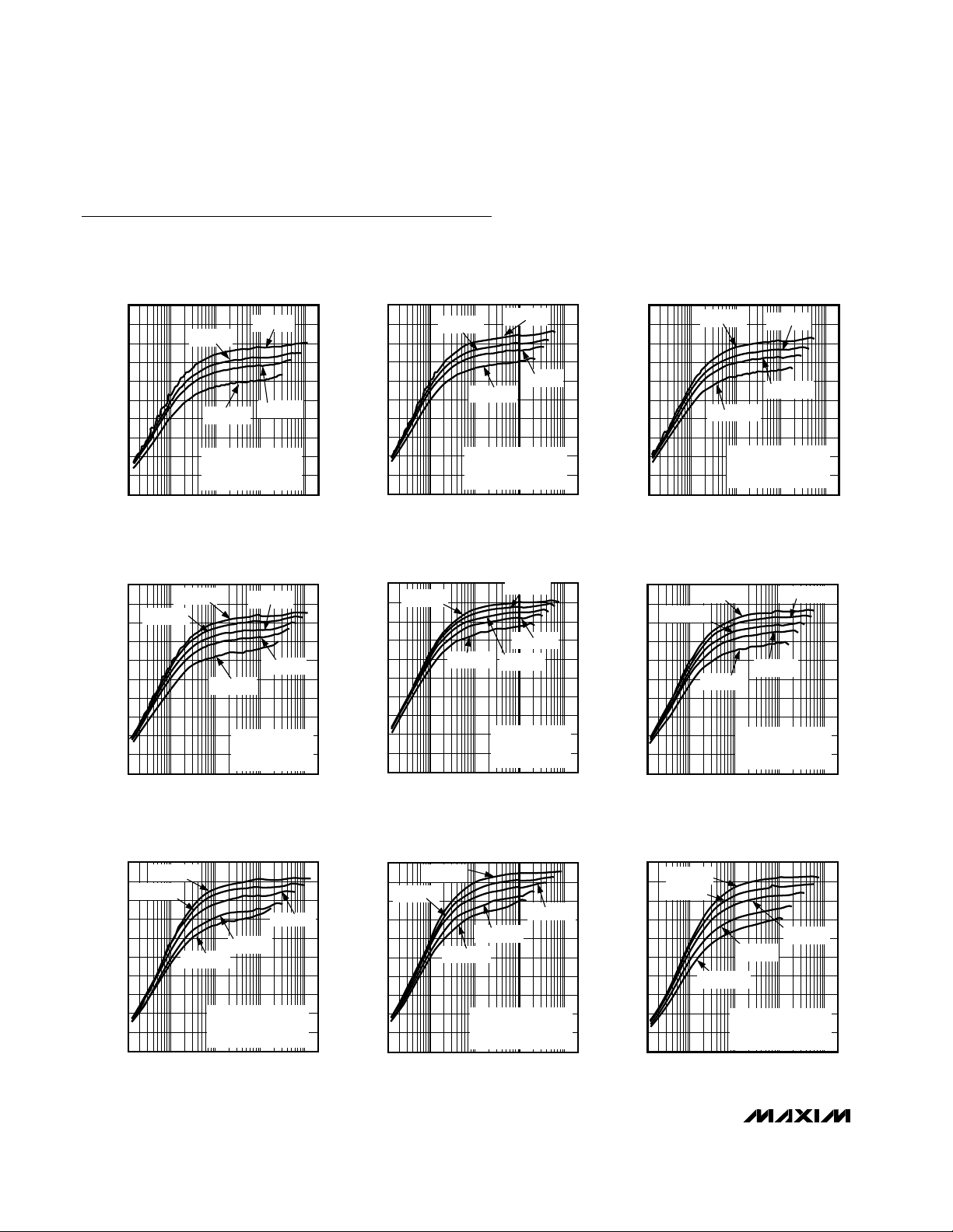
Typical Operating Characteristics
(Circuit of Figure 7 (Fixed Mode, 3.3V) or Figure 8 (Adjustable Mode), TA= +25°C, unless otherwise noted.)
100
0
0.01 0.1 1 10 100
200
EFFICIENCY vs. LOAD CURRENT
(V
OUT
= 2.4V, L1 = 22µH)
20
MAX1678-01
LOAD CURRENT (mA)
EFFICIENCY (%)
40
60
80
90
70
50
30
10
VIN = 2.0V
VIN = 1.5V
L1 = 22µH
SUMIDA CD43-220
R1 = 200kΩ, R2 = 200kΩ
VIN = 1.2V
VIN = 0.85V
100
0
0.01 0.1 1 10 100
200
EFFICIENCY vs. LOAD CURRENT
(V
OUT
= 2.4V, L1 = SUMIDA 47µH)
20
MAX1678-02
LOAD CURRENT (mA)
EFFICIENCY (%)
40
60
80
90
70
50
30
10
VIN = 2.0V
VIN = 1.5V
L1 = 47µH
SUMIDA CD43-470
R1 = 200kΩ, R2 = 200kΩ
VIN = 1.2V
VIN = 0.85V
100
0
0.01 0.1 1 10 100
200
EFFICIENCY vs. LOAD CURRENT
(V
OUT
= 2.4V, L1 = TDK 47µH)
20
MAX1678-03
LOAD CURRENT (mA)
EFFICIENCY (%)
40
60
80
90
70
50
30
10
VIN = 2.0V
VIN = 1.5V
L1 = 47µH
TDK NLC453232T-470K
R1 = 200kΩ, R2 = 200kΩ
VIN = 1.2V
VIN = 0.85V
100
0
0.01 0.1 1 10 100
200
EFFICIENCY vs. LOAD CURRENT
(V
OUT
= 3.3V, L1 = 22µH)
20
MAX1678-04
LOAD CURRENT (mA)
EFFICIENCY (%)
40
60
80
90
70
50
30
10
VIN = 2.5V
VIN = 2.0V
L1 = 22µH
SUMIDA CD43-220
FB = GND
VIN = 1.5V
VIN = 1.2V
VIN = 0.85V
100
0
0.01 0.1 1 10 100
200
EFFICIENCY vs. LOAD CURRENT
(V
OUT
= 5.0V, L1 = 22µH)
20
MAX1678-07
LOAD CURRENT (mA)
EFFICIENCY (%)
40
60
80
90
70
50
30
10
VIN = 4.5V
VIN = 2.0V
L1 = 22µH
SUMIDA CD43-220
R1 = 619kΩ, R2 = 200kΩ
VIN = 3.0V
VIN = 1.2V
VIN = 0.85V
100
0
0.01 0.1 1 10 100
200
EFFICIENCY vs. LOAD CURRENT
(V
OUT
= 3.3V, L1 = SUMIDA 47µH)
20
MAX1678-05
LOAD CURRENT (mA)
EFFICIENCY (%)
40
60
80
90
70
50
30
10
VIN = 2.5V
VIN = 2.0V
L1 = 47µH
SUMIDA CD43-470
FB = GND
VIN = 1.5V
VIN = 1.2V
VIN = 0.85V
100
0
0.01 0.1 1 10 100
200
EFFICIENCY vs. LOAD CURRENT
(V
OUT
= 3.3V, L1 = TDK 47µH)
20
MAX1678-06
LOAD CURRENT (mA)
EFFICIENCY (%)
40
60
80
90
70
50
30
10
VIN = 2.5V
VIN = 2.0V
L1 = 47µH
TDK NLC453232T-470K
FB = GND
VIN = 1.5V
VIN = 1.2V
VIN = 0.85V
100
0
0.01 0.1 1 10 100
200
EFFICIENCY vs. LOAD CURRENT
(V
OUT
= 5.0V, L1 = SUMIDA 47µH)
20
MAX1678-08
LOAD CURRENT (mA)
EFFICIENCY (%)
40
60
80
90
70
50
30
10
VIN = 4.5V
VIN = 3.0V
L1 = 47µH
SUMIDA CD43-470
R1 = 619kΩ, R2 = 200kΩ
VIN = 2.0V
VIN = 1.2V
VIN = 0.85V
100
0
0.01 0.1 1 10 100
200
EFFICIENCY vs. LOAD CURRENT
(V
OUT
= 5.0V, L1 = TDK 47µH)
20
MAX1678-09
LOAD CURRENT (mA)
EFFICIENCY (%)
40
60
80
90
70
50
30
10
VIN = 4.5V
VIN = 3.0V
L1 = 47µH
TDK NLC453232-470K
R1 = 619kΩ, R2 = 200kΩ
VIN = 2.0V
V
IN
= 1.2V
V
IN
= 0.85V
Page 5

MAX1678
1-Cell to 2-Cell, Low-Noise,
High-Efficiency, Step-Up DC-DC Converter
_______________________________________________________________________________________
5
90
50
COILCRAFT
EFFICIENCY WITH DIFFERENT INDUCTORS
55
85
80
DS1608C-473
DT1608C-223
CD43-470
47µH
47µH
47µH
47µH
22µH
47µH
22µH
22µH
CD43-220
LQH4N470K
LQH3C470K
NLC453232T-470K
NLC453232T-220K
MAX1678-10
EFFICIENCY (%)
75
70
65
60
V
BATT
= 1.2V
V
OUT
= 3.3V
I
LOAD
= 20mA
SUMIDA
MURATA
TDK
1000
10
0 0.5 1.0 1.5 2.0 2.5 3.0 3.5 4.0 4.5 5.0
NO-LOAD BATTERY CURRENT
vs. INPUT VOLTAGE
MAX1678-11
INPUT VOLTAGE (V)
NO-LOAD BATTERY CURRENT (µA)
100
V
OUT
= 5.0V
R1 = 3MΩ, R2 = 1MΩ
V
OUT
= 3.0V
FB = GND
L1 = 47µH
SUMIDA CD43-470
V
OUT
= 2.4V
R1 = 1MΩ, R2 = 1MΩ
45
0
-40 100
BATT AND OUT QUIESCENT CURRENT
vs. TEMPERATURE
10
5
40
35
30
MAX1678-12
TEMPERATURE (°C)
QUIESCENT CURRENT (µA)
0-20 80604020
25
20
15
V
BATT
= 1.3V
V
OUT
= 3.6V
FB = GND
I
OUT
I
BATT
12
0
0 6
SHUTDOWN BATTERY CURRENT
vs. INPUT VOLTAGE
2
10
8
MAX1678-13
INPUT VOLTAGE (V)
SHUTDOWN BATTERY CURRENT (µA)
21 543
6
4
3.3V FIXED MODE
L1 = 47µH
SUMIDA CD43-470
140
0
0 5.0
MAXIMUM LOAD CURRENT
vs. INPUT VOLTAGE
(L1 = 22µH)
20
120
100
MAX1678-16
INPUT VOLTAGE (V)
MAXIMUM LOAD CURRENT (mA)
1.51.00.5 4.53.5 4.03.02.52.0
80
60
40
L1 = 22µH
SUMIDA CD43-220
V
OUT
= 3.3V
V
OUT
= 5.0V
V
OUT
= 2.4V
9.0
7.6
-40 100
ON-TIME CONSTANT (K)
vs. TEMPERATURE
7.8
8.8
8.6
MAX1678-14
TEMPERATURE (°C)
ON-TIME CONSTANT (V-µs)
0-20 80604020
8.4
8.2
8.0
V
BATT
= 1.3V
1.3
0.6
0 35
MINIMUM START-UP INPUT VOLTAGE
vs. LOAD CURRENT
0.7
1.2
1.1
MAX1678-15
LOAD CURRENT (mA)
START-UP INPUT VOLTAGE (V)
105 30252015
1.0
0.9
0.8
L1 = 47µH
SUMIDA CD43-470
3.3V FIXED MODE
WITH EXTERNAL
SCHOTTKY DIODE
(FIGURE 3)
WITHOUT
DIODE
140
0
0 5.0
MAXIMUM LOAD CURRENT
vs. INPUT VOLTAGE
(L1 = SUMIDA 47µH)
20
120
100
MAX1678-17
INPUT VOLTAGE (V)
MAXIMUM LOAD CURRENT (mA)
1.51.00.5 4.53.5 4.03.02.52.0
80
60
40
L1 = 47µH
SUMIDA CD43-470
V
OUT
= 5.0V
V
OUT
= 3.3V
V
OUT
= 2.4V
140
0
0 5.0
MAXIMUM LOAD CURRENT
vs. INPUT VOLTAGE
(L1 = TDK 47µH)
20
120
100
MAX1678-18
INPUT VOLTAGE (V)
MAXIMUM LOAD CURRENT (mA)
1.51.00.5 4.53.5 4.03.02.52.0
80
60
40
L1 = 47µH
TDK NLC453232T-470K
V
OUT
= 5.0V
V
OUT
= 3.3V
V
OUT
= 2.4V
Typical Operating Characteristics (continued)
(Circuit of Figure 7 (Fixed Mode, 3.3V) or Figure 8 (Adjustable Mode), TA= +25°C, unless otherwise noted.)
Page 6

MAX1678
1-Cell to 2-Cell, Low-Noise,
High-Efficiency, Step-Up DC-DC Converter
6 _______________________________________________________________________________________
A
B
C
SWITCHING WAVEFORM
MAX1678-19
V
OUT
= 3.3V, V
BATT
= 1.2V, I
LOAD
= 10mA, C
OUT
= 10µF,
L1 = SUMIDA CD43-470
A: LX, 2V/div B: V
OUT
, 50mV/div AC COUPLED
C: INDUCTOR CURRENT, 100mA/div
5µs/div
Typical Operating Characteristics (continued)
(Circuit of Figure 7 (Fixed Mode, 3.3V) or Figure 8 (Adjustable Mode), TA= +25°C, unless otherwise noted.)
Pin Description
PIN
Battery-Power InputBATT1
FUNCTIONNAME
Power-Fail Input. When the voltage at PFI is below 614mV, PFO sinks current.PFI2
Active-Low Shutdown. Connect SHDN to BATT for normal operation.SHDN
4
Open-Drain Power-Fail Output. PFO sinks current when PFI is below 614mV.PFO3
GroundGND6
Power Output and IC Power Input (bootstrapped). OUT is the feedback input for 3.3V operation. Connect
the filter capacitor close to OUT.
OUT8
N-Channel MOSFET Switch Drain and P-Channel Synchronous-Rectifier DrainLX7
Dual-Mode Feedback Input. Connect FB to GND for fixed-output operation (3.3V). Connect FB to a feedback-resistor network for adjustable output voltage operation (2V to 5.5V). FB regulates to 1.23V.
FB5
LOAD-TRANSIENT RESPONSE
A
MAX1678-20
A
B
V
= 3.3V, V
OUT
L1 = SUMIDA CD43-470
A: V
OUT
LINE-TRANSIENT RESPONSE
MAX1678-21
200µs/div
= 1.2V, I
BATT
, 50mV/div, AC COUPLED B: VIN, 1V/div, 1.2V to 2.2V
LOAD
= 10mA, C
OUT
= 10µF,
B
C
100µs/div
V
= 3.3V, V
OUT
L1 = SUMIDA CD43-470,
A: V
OUT
C: LOAD, 2mA to 12mA 100mA/div
= 1.2V, C
BATT
, 50mV/div, AC COUPLED B: INDUCTOR CURRENT,
OUT
= 10µF,
POWER-UP RESPONSE
A
B
C
100µs/div
V
= 3.3V, V
OUT
L1 = SUMIDA CD43-470
A: V
OUT
C: SHDN, 5V/div
= 1.2V, I
BATT
, 1V/div B: INDUCTOR CURRENT, 100mA/div
LOAD
= 10mA, C
OUT
MAX1678-22
= 10µF,
Page 7

MAX1678
1-Cell to 2-Cell, Low-Noise,
High-Efficiency, Step-Up DC-DC Converter
_______________________________________________________________________________________ 7
Detailed Description
The MAX1678 consists of an internal 1Ω, N-channel
MOSFET power switch, a built-in synchronous rectifier
that acts as the catch diode, a reference, PFM control
circuitry, and an inductor damping switch (Figure 1).
The device is optimized for applications that are powered by 1 to 3-cell alkaline, NiMH, or NiCd batteries, or
a 1-cell lithium battery such as pagers, remote controls,
and battery-powered instruments. They are designed to
meet the specific demands of the operating states
characteristic of such systems:
1)
Primary battery is good and load is active:
In this
state the load draws tens of milliamperes and the
MAX1678 typically offers 80% to 90% efficiency.
2)
Primary battery is good and load is sleeping:
In this
state the load draws hundreds of microamperes and
the DC-DC converter IC draws very low quiescent
current. Many applications maintain the load in this
state most of the time.
3)
Primary battery is dead and DC-DC converter is
shut down:
In this state the load is sleeping or supplied by the backup battery, and the MAX1678
draws 0.1µA current from the OUT pin.
4)
Primary and backup battery dead:
The DC-DC con-
verter can restart from this condition.
BATT
PFI
0.5REF
PFO
GND
OUT
REF
N
P
OUT 1.7V
FB
SHDN
LX
RFRDY
1.23V REF
REF
START-UP COMPARATOR
0.5REF
START-UP
OSCILLATOR
EN
DAMP
TON TOFF
PDRV
CONTROL LOGIC
MAX1678
tON = K/V
BATT
BACKUP t
OFF
TIMER
DAMPING
SWITCH
ZERO-CROSSING
DETECTION
NDRV
Figure 1. Functional Diagram
Page 8

MAX1678
Operating Principle
The MAX1678 employs a proprietary constant-peakcurrent control scheme that combines the ultra-low quiescent current of traditional pulse-skipping PFM
converters with high-load efficiency.
When the error comparator detects that the output voltage is too low, it turns on the internal N-channel
MOSFET switch for an internally calculated on-time
(Figure 2). During the on-time, current ramps up in the
inductor, storing energy in the magnetic field. When the
MOSFET turns off during the second half of each cycle,
the magnetic field collapses, causing the inductor voltage to force current through the synchronous rectifier,
transferring the stored energy to the output filter
capacitor and the load. The output filter capacitor
stores charge while the current from the inductor is
high, then holds up the output voltage until the second
half of the next switching cycle, smoothing power flow
to the load. The ideal on-time of the N-channel MOSFET
changes as a function of input voltage. The on-time is
determined as follows:
where K is typically 8V-µs.
The peak inductor current (assuming a lossless circuit)
can be calculated from the following equation:
The P-channel MOSFET (synchronous rectifier) turns on
when the N-channel MOSFET turns off. The circuit operates at the edge of discontinuous conduction; therefore,
the P-channel synchronous rectifier turns off immediately
after the inductor current ramps to zero. During the dead
time after the P-switch has been turned off, the damping
switch connects LX and BATT. This suppresses EMI noise
due to LC ringing of the inductor and parasitic capacitance at the LX node (see
Damping Switch
section). The
error comparator starts another cycle when V
OUT
falls
below the regulation threshold. With this control scheme,
the MAX1678 maintains high efficiency over a wide range
of loads and input/output voltages while minimizing
switching noise.
Start-Up Operation
The MAX1678 contains a low-voltage start-up oscillator
(Figure 1). This oscillator pumps up the output voltage
to approximately 1.7V, the level at which the main DCDC converter can operate. The 150kHz fixed-frequency
oscillator is powered from the BATT input and drives an
NPN switch. During start-up, the P-channel synchronous
rectifier remains off and its body diode (or an external
diode, if desired) is used as an output rectifier. The minimum start-up voltage is a function of load current (see
Typical Operating Characteristics
). In normal operation,
when the voltage at the OUT pin exceeds 1.7V, the DCDC converter is powered from the OUT pin (bootstrapped) and the main control circuitry is enabled.
Once started, the output can maintain the load as the
battery voltage decreases below the start-up voltage.
To improve start-up capability with heavy loads, add a
Schottky diode in parallel with the P-channel synchronous rectifier (from LX to OUT) as shown in Figure 3
(see
Typical Operating Characteristics
).
I =
K
L
PEAK
t =
K
V
ON
BATT
1-Cell to 2-Cell, Low-Noise,
High-Efficiency, Step-Up DC-DC Converter
8 _______________________________________________________________________________________
V
LX
V
BATT
(DEAD TIME)
(DEAD TIME)
I
PEAK
=
K
L
(ON TIME)
(ON TIME)
t
V
OUT
V
BATT
K
V
OUT
- V
BATT
I
L
t
I
PEAK
t
ON
t
ON
OR DEAD TIME
t
OFF
K
V
BATT
Figure 2. Switching Waveforms
MAX1678
PDRV
NDRV
TIMING
CIRCUIT
V
OUT
C
OUT
V
IN
L1
OUT
LX
GND
P
N
START-UP
OSCILLATOR
Figure 3. External Schottky Diode to Improve Start-Up with
Heavy Load
Page 9

Shutdown Mode
Pulling the SHDN pin low places the MAX1678 in shutdown mode (I
SHDN
= 2µA typical). In shutdown, the
internal switching MOSFET turns off, PFO goes high
impedance, and the synchronous rectifier turns off to
prevent the flow of reverse current from the output back
to the input. However, there is still a forward current
path through the synchronous-rectifier body diode from
the input to the output. Thus, in shutdown, the output
remains one diode drop below the battery voltage
(V
BATT
).
To disable the shutdown feature, connect SHDN (a
logic input) to BATT or OUT.
Reverse-Battery Protection
The MAX1678 can sustain/survive battery reversal up to
the package power-dissipation limit. An internal 5Ω
resistor in series with a diode limits reverse current to
less than 220mA, preventing damage. Prolonged operation above 220mA reverse-battery current can
degrade the device’s performance.
Power-Fail Comparator
The MAX1678 has an on-chip comparator for power-fail
detection. This comparator can detect a loss of power
at the input or output (Figures 7 and 8). If the voltage at
the power-fail input (PFI) falls below 614mV, the PFO
output sinks current to GND. Hysteresis at PFI is 2%.
The power-fail monitor threshold is set by two resistors,
R3 and R4, using the following equation:
where VTHis the desired threshold of the power-fail
detector, and V
PFI
is the 614mV threshold of the powerfail comparator. Since PFI leakage is 10nA max, select
feedback resistor R4 in the 100kΩ to 1MΩ range.
Damping Switch
The MAX1678 is designed with an internal damping
switch to minimize ringing at the LX node. The damping
switch (Figure 4) connects the LX node to BATT, effectively depleting the inductor’s remaining energy. When
the energy in the inductor is insufficient to supply current to the output, the capacitance and inductance at
LX form a resonant circuit that causes ringing. The
damping switch supplies a path to quickly dissipate
this energy, suppressing the ringing at LX. This does
not reduce the output ripple, but does reduce EMI.
Figures 5 and 6 show the LX node voltage waveform
without and with the damping switch.
R3 = R4 x
V
V
TH
PFI
−
1
MAX1678
1-Cell to 2-Cell, Low-Noise,
High-Efficiency, Step-Up DC-DC Converter
_______________________________________________________________________________________ 9
MAX1678
PDRV
DAMP
NDRV
TIMING
CIRCUIT
OUT
V
OUT
V
IN
BATT
LX
DAMPING
SWITCH
GND
P
P
N
Figure 4. Simplified Diagram of Damping Switch
2µs/div
1V/div
V
BATT
= 2.5V
V
OUT
= 3.3V
L1 = 47µH
Figure 5. LX Ringing Without Damping Switch (example only)
Figure 6. LX Ringing With Damping Switch
2µs/div
1V/div
V
BATT
= 1.8V
V
OUT
= 3.3V
L1 = 47µH
Page 10

MAX1678
Applications Information
Output Voltage Selection
The MAX1678 operates with a fixed 3.3V or adjustable
output. To select fixed-voltage operation, connect FB to
GND (Figure 7). For an adjustable output between 2V
and 5.5V, connect FB to a resistor voltage-divider
between OUT and GND (Figure 8). FB regulates to
1.23V.
Since FB leakage is 10nA max, select feedback resistor
R2 in the 100kΩ to 1MΩ range. R1 is given by:
where V
REF
= 1.23V.
Maximum Output Current
and Inductor Selection
The MAX1678 is designed to work well with a 47µH
inductor in most low-power applications. 47µH is a sufficiently low value to allow the use of a small surfacemount coil, but large enough to maintain low ripple. The
Typical Operating Characteristics
section shows performance curves with several 47µH and 22µH coils. Low
inductance values supply higher output current but
also increase ripple and reduce efficiency. Note that
values below 22µH are not recommended due to
MAX1678 switch limitations. Higher inductor values
reduce peak inductor current (and consequent ripple
and noise) and improve efficiency, but also limit output
current.
The relationship between current and inductor value is
approximately:
where M is an empirical factor that takes into account
losses in the MAX1678 internal switches and in the
inductor resistance. K is the V-µs factor that governs
the inductor charge time. Nominally, M = 0.9 and
K = 8V-µs. M should be further reduced by 0.1 for each
ohm of inductor resistance.
The inductor’s saturation-current rating must exceed
the worst-case peak current limit set by the MAX1678’s
timing algorithm:
where K
MAX
= 11.2V-µs. It is usually acceptable to
exceed most coil saturation-current ratings by 20% with
no ill effects; however, the maximum recommended I
PEAK
for the MAX1678 internal switches is 550mA, so inductor
values below 22µH are not recommended. For optimum
efficiency, inductor series resistance should be less than
150mV/I
PEAK
. Table 1 lists suggested inductors and sup-
pliers.
Table 1. Suggested Inductors and Suppliers
I
K
L
PEAK
MAX
=
I M x x
K
L
x
V
V
OUT MAX
BATT
OUT
( )
=
1
2
R1 = R2 x
V
V
OUT
REF
−
1
1-Cell to 2-Cell, Low-Noise,
High-Efficiency, Step-Up DC-DC Converter
10 ______________________________________________________________________________________
MAX1678
GND FB
BATT
PFI
3.3V
OUT
INPUT
0.87V TO V
OUT
L1
47µH, 200mA
PFO
C2
10µF
SHDN
LX
OUT
OUT
C1
10µF
R3
R4
R5
Figure 7. 3.3V Standard Application Circuit
Figure 8. Adjustable Output Circuit
MAX1678
GND
BATT
PFI
V
OUT
= 2V
TO 5.5V
INPUT
0.87V TO V
OUT
L1
47µH
PFO
SHDN
LX
OUT
FB
R1
C2
R2
OUT
C1
10µF
R4 R5
R3
LQH4N470K,
LQH3C470K
Murata
NLC453232T-220K,
NLC453232T-470K
TDK
CD43-220,
CD43-470
Sumida
PIN
DS1608C-223,
DS1608C-473
Coilcraft
INDUCTOR
(814) 237-1431
(847) 390-4373
(847) 956-0666
(847) 639-6400
PHONE
Page 11

Capacitor Selection
Choose input and output capacitors to service input
and output peak currents with acceptable voltage ripple. Capacitor ESR is a major contributor to output ripple (usually more than 60%). A 10µF, ceramic output
filter capacitor typically provides 50mV output ripple
when stepping up from 1.3V to 3.3V at 20mA. Low input
to output voltage differences (i.e., 2 cells to 3.3V)
require higher capacitor values (10µF to 47µF).
The input filter capacitor (CIN) also reduces peak currents drawn from the battery and improves efficiency.
Low-ESR capacitors are recommended. Ceramic
capacitors have the lowest ESR, but low-ESR tantalums
represent a good balance between cost and performance. Low-ESR aluminum electrolytic capacitors are
tolerable, and standard aluminum electrolytic capacitors should be avoided. Capacitance and ESR variation
over temperature need to be taken into consideration
for best performance in applications with wide operating temperature ranges. Table 2 lists suggested capacitors and suppliers.
Minimizing Noise and Voltage Ripple
EMI and output voltage ripple can be minimized by following these simple design rules:
1) Place the DC-DC converter and digital circuitry on
the opposite corner of the PC board from sensitive
RF and analog input stages.
2) Use a closed-core inductor, such as toroid or
shielded bobbin, to minimize fringe magnetic fields.
3) Choose the largest inductor value that satisfies the
load requirement, to minimize peak switching current and the resulting ripple and noise.
4) Use low-ESR input and output filter capacitors.
5) Follow sound circuit-board layout and grounding
rules (see the
PC Board Layout and Grounding
sec-
tion).
PC Board Layout and Grounding
High switching frequencies and large peak currents
make PC board layout an important part of design.
Poor design can result in excessive EMI on the feedback paths and voltage gradients in the ground plane.
Both of these factors can result in instability or regulation errors. The OUT pin must be bypassed directly to
GND, as close to the IC as possible (within 0.2 inches
or 5mm).
Place power components—such as the MAX1678,
inductor, input filter capacitor, and output filter capacitor—as close together as possible. Keep their traces
short, direct, and wide (≥50 mil or 1.25mm), and place
their ground pins close together in a star-ground configuration. Keep the extra copper on the board and
integrate it into ground as a pseudo-ground plane. On
multilayer boards, route the star ground using component-side copper fill, then connect it to the internal
ground plane using vias.
Place the external voltage-feedback network very close
to the FB pin (within 0.2 inches or 5mm). Noisy traces,
such as from the LX pin, should be kept away from the
voltage-feedback network and separated from it using
grounded copper. The MAX1678 evaluation kit manual
shows an example PC board layout, which includes a
pseudo-ground plane.
MAX1678
1-Cell to 2-Cell, Low-Noise,
High-Efficiency, Step-Up DC-DC Converter
______________________________________________________________________________________ 11
Table 2. Recommended Surface-Mount Capacitor Manufacturers
603-224-1961
PHONE
VALUE
(µF)
595D-series tantalum
DESCRIPTION
Sprague
MANUFACTURER
803-946-0690AVXTAJ, TPS-series tantalum
4.7 to 47
803-946-0690AVX
X7R ceramic4.7 to 10
847-390-4373TDK
X7R ceramic4.7 to 22 408-573-4150Taiyo Yuden
Page 12

MAX1678
1-Cell to 2-Cell, Low-Noise,
High-Efficiency, Step-Up DC-DC Converter
12 ______________________________________________________________________________________
Package Information
___________________Chip Information
TRANSISTOR COUNT: 840
8LUMAXD.EPS
 Loading...