

Page 1
For free samples & the latest literature: http://www.maxim-ic.com, or phone 1-800-998-8800.
For small orders, phone 1-800-835-8769.
General Description
The MAX1666 provides complete protection against overvoltage, undervoltage, overcharge current, overdischarge
current, and cell mismatch for 2-cell to 4-cell Lithium-Ion
battery packs. The voltage of each cell in the battery pack
is checked and compared to the programmable threshold
and to the other cells in the pack.
The MAX1666 protects the battery pack in an overcurrent
condition by disconnecting the pack from the load at a programmable limit. On-chip power MOSFET drivers control
external P-channel MOSFETs to disconnect the cells from
external terminals when faults occur.
The MAX1666 employs a unique timing scheme that allows
three modes of operation, for optimal performance and battery power conservation. The MAX1666 can operate in a
stand-alone configuration or in conjunction with a microcontroller. It is available in three versions: the “S” version
monitors two Li-Ion cells, the “V” version monitors three
cells, and the “X” version monitors four cells.
Applications
2/3/4-Cell Lithium-Ion Battery Pack
Features
♦ Overvoltage Protection
Programmable Limits from +4.0V to +4.4V
Accurate to ±0.5%
♦ Undervoltage Protection
Programmable Limits from +2.0V to +3.0V
Accurate to ±2.5%
♦ Cell Mismatch Protection
Programmable Limits from 0 to 500mV
Accurate to ±10%
♦ Overcharge Current Protection
♦ Overdischarge Current Protection
♦ Low Operating Supply Current: 30µA typ
♦ Low Standby Current: 1µA max
♦ +28V max Input Voltage
♦ Available in Small 16-Pin QSOP (MAX1666S) and
20-Pin QSOP (MAX1666V/X) Packages
MAX1666S/V/X
Advanced Lithium-Ion
Battery-Pack Protector
________________________________________________________________
Maxim Integrated Products
1
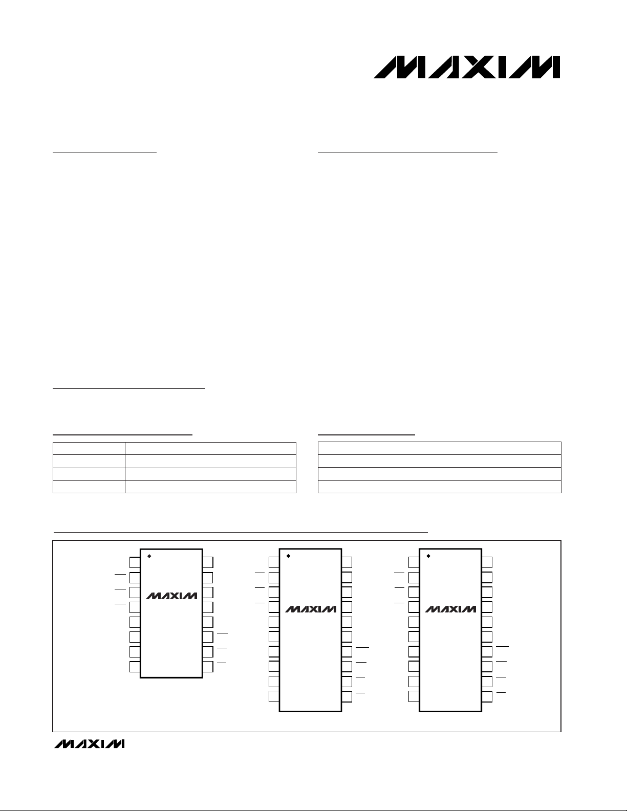
TOP VIEW
20
19
18
17
16
15
14
13
1
2
3
4
5
6
7
8
UVO
V
CC
REF
OVACGO
TKO
DSO
SRC
UVA
MMA
WRN
PKFB1P
B2P
B3P
B3P
12
11
9
10
CGI
DSIPKN
GND
MAX1666V
20
19
18
17
16
15
14
13
1
2
3
4
5
6
7
8
UVO
V
CC
REF
OVACGO
TKO
DSO
SRC
UVA
MMA
WRN
PKFB1P
B2P
B3P
B4P
12
11
9
10
CGI
DSIPKN
GND
MAX1666X
16
15
14
13
12
11
10
9
1
2
3
4
5
6
7
8
SRC V
CC
REF
OVA
UVA
MMA
PKF
CGI
DSI
MAX1666S
DSO
TKO
BIP
CGO
B2P
GND
PKN
QSOP
QSOP QSOP
19-1465; Rev 1; 7/99
PART
MAX1666SEEE
MAX1666VEEP
MAX1666XEEP -40°C to +85°C
-40°C to +85°C
-40°C to +85°C
TEMP. RANGE PIN-PACKAGE
16 QSOP
20 QSOP
20 QSOP
Pin Configurations
Ordering Information
Selector Guide
Typical Operating Circuits appear at end of data sheet.
NUMBER OF LI-ION CELLSPART
MAX1666S 2
3
4MAX1666X
MAX1666V
Page 2
MAX1666S/V/X
Advanced Lithium-Ion
Battery-Pack Protector
2 _______________________________________________________________________________________
ABSOLUTE MAXIMUM RATINGS
ELECTRICAL CHARACTERISTICS
(V
SRC
= 16V, each cell voltage V
CELL
= 3.6V, 330kΩ load at REF, TA= 0°C to +85°C, unless otherwise noted. Typical values are at
T
A
= +25°C.)
Stresses beyond those listed under “Absolute Maximum Ratings” may cause permanent damage to the device. These are stress ratings only, and functional
operation of the device at these or any other conditions beyond those indicated in the operational sections of the specifications is not implied. Exposure to
absolute maximum rating conditions for extended periods may affect device reliability.
SRC, DSO, TKO, CGO, UVO, PKF, WRN to GND ...-0.3V to +28V
V
CC
, REF, OVA, UVA, MMA to GND ........................-0.3V to +6V
B4P to B3P ...............................................................-0.3V to +6V
B3P to B2P ...............................................................-0.3V to +6V
B2P to B1P ...............................................................-0.3V to +6V
B1P to GND..............................................................-0.3V to +6V
PKN to GND...........................................................................±2V
V
CC
, CGI, DSI to PKN...............................................-0.3V to +6V
Continuous Power Dissipation (T
A
= +70°C)
16-Pin QSOP (derate 8.3mW/°C above +70°C)...........667mW
20-Pin QSOP (derate 9.1mW/°C above +70°C)...........727mW
Operating Temperature Range ...........................-40°C to +85°C
Storage Temperature Range .............................-65°C to +150°C
Lead Temperature (soldering, 10sec) .............................+300°C
No faults, long time average current from
the top battery terminal B_P
V
SRC
- V
B_P
= 1V
V
SRC
- V
B_P
R
LOAD
≥ 665Ω, 2V < V
CELL
< 4.4V
Pulse on
CONDITIONS
µA
30 45
I
SUP
Supply Current
µA
210
V
1
Charge Mode Detection Threshold
SRC Input Current Range
µA1I
SHDN
Shutdown Supply Current
V3.09 3.25 3.41V
CC
VCCOutput Voltage
V2.7 2.85 3
VCCUndervoltage Lockout
Threshold
V1.221V
REF
Reference Output Voltage
UNITSMIN TYP MAXSYMBOLPARAMETER
Cell voltage rising
Cell voltage falling
4.378 4.400 4.422
V4.2
3.980 4.000 4.020
Overvoltage Threshold
mV200Overvoltage Threshold Hysteresis
V
1.950 2.000 2.050
Undervoltage Threshold 2.500
2.925 3.000 3.075
OVA, UVA, MMA = REF
Above undervoltage threshold,
cell voltage falling
mV
All cells > 2V
-220 -200 -180
PKN to GND Overcharge Current
Threshold
nA0.1 20OVA, UVA, MMA Input Current
mV100
mV100Undervoltage Threshold Hysteresis
WRN Early Warning Threshold
mV
±0
Cell Mismatch Threshold
±250
±450 ±500 ±550
mV270 300 330
PKN to GND Overdischarge
Current Threshold
OVA = GND
V
OVA
= V
REF
/ 2
OVA = REF
UVA = GND
V
UVA
= V
REF
/ 2
UVA = REF
MMA = GND
V
MMA
= V
REF
/ 2
MMA = REF
mV200
WRN Early Warning Threshold
Hysteresis
Page 3
MAX1666S/V/X
Advanced Lithium-Ion
Battery-Pack Protector
_______________________________________________________________________________________ 3
No faults, long time average current from the
top battery terminal B_P
V
SRC
- V
B_P
= 1V to 4V
V
SRC
- V
B_P
4.373 4.427
R
LOAD
≥ 665Ω, 2V < V
CELL
< 4.4V
3.975 4.025
CONDITIONS
Overvoltage Threshold
OVA, UVA, MMA = REF
µA
45
I
SUP
Supply Current
µA
10
V
1
Charge Mode Detection
Threshold
SRC Input Current Range
nA20OVA, UVA, MMA Leakage
µA1I
SHDN
Shutdown Supply Current
V3.09 3.41V
CC
VCCOutput Voltage
V2.7 3
VCCUndervoltage Lockout
Threshold
UNITSMIN TYP MAXSYMBOLPARAMETER
OVA = GND
OVA = REF
V
V
2.925 3.075
1.950 2.050
Undervoltage Threshold
UVA = GND
UVA = REF
CONDITIONS
No faults, V
DSO
= V
CGO=VUVO
= 1V to 27V
V
DSO
= V
SRC
- 4V and V
CGO
= V
SRC
- 4V,
fault condition
V
DSO
= V
CGO
= V
UVO
= 27V, fault condition
ms1.6 2.4 3.2t
I-DELAY
Overdischarge/Overcharge
Current Fault Blanking Time
ms330 550 770t
P-DELAY
Overcurrent Fault Timer Delay
µA20 30 40
DSO, CGO, UVO Output Sink
Current
mA210
DSO, CGO Output Source
Current
µA0.2
DSO, CGO, UVO Leakage
Current
UNITSMIN TYP MAXSYMBOLPARAMETER
V
DSI
, V
CGI
= 5V
Referenced to PKN
Referenced to PKN
Fault condition, V
WRN
= 0.4V
Fault condition, V
PKF
= 0.4V
V
PKF
= V
WRN
= 27V
µA1
DSI, CGI Input Current
V0.45
V2
TKO = GND
DSI, CGI Input High Voltage
DSI, CGI Input Low Voltage
mA24
WRN Sink Current
mA48
PKF Sink Current
µA0.2
PKF, WRN Leakage Current
kΩ100 200
TKO Pull-Down Resistance
mA18
TKO Source Current
Fault persistent for 4 consecutive sample
periods
ms180 320 460t
F-DELAY
Undervoltage, Overvoltage, or
Mismatch Fault, to DSO, CGO,
TKO Transition Delay
ELECTRICAL CHARACTERISTICS (continued)
(V
SRC
= 16V, each cell voltage V
CELL
= 3.6V, 330kΩ load at REF, TA= 0°C to +85°C, unless otherwise noted. Typical values are at
T
A
= +25°C.)
ELECTRICAL CHARACTERISTICS
(V
SRC
= 16V, each cell voltage V
CELL
= 3.6V, 330kΩ load at REF, TA= -40°C to +85°C, unless otherwise noted.) (Note 1)
Page 4

MAX1666S/V/X
Advanced Lithium-Ion
Battery-Pack Protector
4 _______________________________________________________________________________________
CONDITIONS
No faults; V
DSO
, V
CGO
, V
UVO
= 1V to 27V
V
DSO
= V
SRC
- 4V and V
CGO
= V
SRC
- 4V,
fault condition
V
DSO
= V
CGO
= V
UVO
= 27V, fault condition
ms1.6 3.2t
I-DELAY
Overdischarge/Overcharge
Current Fault Blanking Time
ms330 770t
P-DELAY
mV
All cells > 2V, MMA = REF
-220 -180
PKN to GND Overcharge
Current Threshold
Overcurrent Fault Timer Delay
µA20 40
DSO, CGO UVO Output Sink
Current
mA2
DSO, CGO Output Source
Current
µA0.2
DSO, CGO, UVO Leakage
Current
UNITSMIN TYP MAXSYMBOLPARAMETER
mV±450 ±550Cell Mismatch Threshold
mV270 330
PKN to GND Overdischarge
Current Threshold
V
DSI
= V
CGI
= 5V
Referenced to PKN
Referenced to PKN
Fault condition, V
WRN
= 0.4V
Fault condition, V
PKF
= 0.4V
V
PKF
= V
WRN
= 27V
µA1
DSI, CGI Input Current
V0.45
V2
TKO = GND
DSI, CGI Input High Voltage
DSI, CGI Input Low Voltage
mA2
WRN Sink Current
mA4
PKF Sink Current
µA0.2
PKF, WRN Leakage Current
kΩ100
TKO Pull-Down Resistance
mA1
TKO Source Current
Fault persistent for 4 consecutive sample
periods
ms180 460t
F-DELAY
Undervoltage, Overvoltage, or
Mismatch Fault, to DSO, CGO,
TKO Transition Delay
Note 1: Specifications to -40°C are guaranteed by design, not production tested.
ELECTRICAL CHARACTERISTICS
(V
SRC
= 16V, each cell voltage V
CELL
= 3.6V, 330kΩ load at REF, TA= -40°C to +85°C, unless otherwise noted.) (Note 1)
Page 5
MAX1666S/V/X
Advanced Lithium-Ion
Battery-Pack Protector
_______________________________________________________________________________________
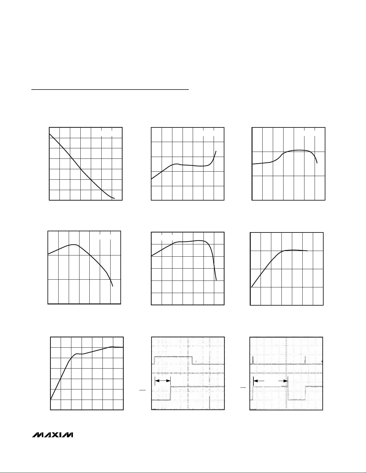
5
700
720
710
740
730
760
750
770
-40 0 20-20 40 60 80 100
SHUTDOWN SUPPLY CURRENT
vs. TEMPERATURE
MAX1666toc01
TEMPERATURE (°C)
SUPPLY CURRENT (nA)
V
CELL
= 3.6V
25
27
31
29
33
35
-40 0 20-20 40 60 80 100
SUPPLY CURRENT
vs. TEMPERATURE
MAX1666toc02
TEMPERATURE (°C)
SUPPLY CURRENT (µA)
V
CELL
= 3.6V
3.0000
3.0005
3.0010
3.0015
UNDERVOLTAGE THRESHOLD
vs. TEMPERATURE
MAX1666toc03
TEMPERATURE (°C)
UNDERVOLTAGE THRESHOLD (V)
-40 20 40-20 0 60 80 100
UVA = REF
4.385
4.390
4.395
4.400
OVERVOLTAGE THRESHOLD
vs. TEMPERATURE
MAX1666toc04
TEMPERATURE (°C)
UNDERVOLTAGE THRESHOLD (V)
-40 20 40-20 0 60 80 100
OVA = REF
295
297
296
299
298
301
300
302
-40 0 20-20 40 60 80 100
OVERDISCHARGE THRESHOLD
vs. TEMPERATURE
MAX1666toc07
TEMPERATURE (°C)
OVERDISCHARGE THRESHOLD (mV)
495
497
496
499
498
500
501
-40 20 40-20 0 60 80 100
MISMATCH VOLTAGE THRESHOLD
vs. TEMPERATURE
MAX1666toc05
TEMPERATURE (°C)
MISMATCH VOLTAGE THRESHOLD (mV)
MMA = REF
199
200
201
202
203
OVERCHARGE THRESHOLD
vs. TEMPERATURE
MAX1666toc06
TEMPERATURE (°C)
OVERCHARGE THRESHOLD (mV)
-40 20 40-20 0 60 80 100
1ms/div
OVERDISCHARGE PROTECTION
PKN
(0.5V/div)
DSO
(10V/div)
MAX1666toc08
t
I-DELAY
100ms/div
OVERDISCHARGE RECOVERY TIME
(0.5V/div)
(10V/div)
PKN
DSO
MAX1666toc09
t
P
Typical Operating Characteristics
(TA = +25°C, unless otherwise noted.)
Page 6

MAX1666S/V/X
Advanced Lithium-Ion
Battery-Pack Protector
6 _______________________________________________________________________________________
100ms/div
OVERCHARGE
(0.5V/div)
(10V/div)
PKN
CGO
MAX1666toc10
t
P-DELAY
Typical Operating Characteristics (continued)
(TA= +25°C, unless otherwise noted.)
100ms/div
OVERVOLTAGE FAULT
4.1V
(1V/div)
4.5V
123 4 123 4
REF
B1P
MAX1666toc11
(10V/div)
CGO
t
F-DELAY
t
F-DELAY
V
CELL2
= V
CELL3
= V
CELL4
= 4.15V,
OVERVOLTAGE THRESHOLD = 4.4V
100ms/div
UNDERVOLTAGE FAULT
3.4V
2.9V
(10V/div)
(1V/div)
(10V/div)
REF
B1P
DSO
MAX1666toc12
WRN
t
F-DELAY
t
F-DELAY
V
CELL2
= V
CELL3 = VCELL4
= 3.35V,
UNDERVOLTAGE THRESHOLD = 3.0V,
UVA = REF
1234 1234
100ms/div
CELL MISMATCH FAULT
3.4V
2.9V
32141234
(10V/div)
(1V/div)
(10V/div)
REF
B1P
DSO
MAX1666toc13
PKF
t
F-DELAY
t
F-DELAY
V
CELL2
= V
CELL3 = VCELL4
= 3.6V,
CELL MISMATCH THRESHOLD = 0.5V,
100ms/div
UNDERVOLTAGE FAULT WITHOUT
CHARGE SOURCE (V
SRC
< V
B4P
+ 1V)
V
CELL2
= V
CELL3 = VCELL4
= 3.35V,
UNDERVOLTAGE THRESHOLD = 3.0V,
UVA = REF
3.4V
2.9V
(1V/div)
(10V/div)
(2V/div)
REF
B1P
V
CC
DSO
MAX1666toc14
Page 7

Pin Description
MAX1666S/V/X
Advanced Lithium-Ion
Battery-Pack Protector
_______________________________________________________________________________________ 7
Cell 1 Positive Input88
Ground99
Battery Pack Negative Terminal. Connect to bottom of current sense
resistor. Ground reference for logic inputs DSI and CGI.
1010
Discharge Control Input 1111
Charge Control Input 1212
Fast-Charge Driver Output. Drives external P-channel MOSFET to
control fast charge.
44
Cell 4 Positive Input. Power supply input for MAX1666X.
—
5
Cell 3 Positive Input. Power supply input for MAX1666V.5, 6 6
Cell 2 Positive Input. Power supply input for MAX1666S.77
Trickle-Charge Driver Output. Drives external P-channel MOSFET to
control trickle-charge current. Internally grounded when inactive.
3 3
Discharge Driver Output. Drives external P-channel MOSFET to control discharge.
22
Charge Source Input. Provides current for gate drivers DSO, TKO,
CGO, and UVO.
11
MAX1666VMAX1666X
FUNCTION
Pack Fail Output. PKF goes low when any cell voltage exceeds the
mismatch threshold or when a shorted cell is detected.
1313
Undervoltage/Overvoltage Warning Output1414
6
7
8
9
10
4
—
—
5
3
2
1
MAX1666S
11
—
B1P
GND
PKN
DSI
CGI
CGO
B4P
B3P
B2P
TKO
DSO
SRC
NAME
PKF
WRN
Undervoltage Adjust Input. Set the undervoltage threshold with a
resistor-divider from REF to GND.
1616
Overvoltage Adjust Input. Set the overvoltage threshold with a
resistor-divider from REF to GND.
1717
Reference Voltage Output. Minimize PCB stray capacitance on this
node.
1818
3.3V Linear Regulator Output. Bypass with a 0.47µF min capacitor
to GND.
1919
Undervoltage Fault Output2020
Mismatch Adjust Input. Set the mismatch threshold by a resistordivider from REF to GND.
1515
13
14
15
16
—
12
UVA
OVA
REF
V
CC
UVO
MMA
PIN
Page 8

MAX1666S/V/X
Advanced Lithium-Ion
Battery-Pack Protector
8 _______________________________________________________________________________________
BIAS
B4P
CQI_FAULT
550ms
TIMER
SET/RESET
WARNING
OV-FAULT
UV-FAULT
CM-FAULT
PKF
WRN
V
CC
DQI_FAULT
TKO
N
SRC
SRC
SRC
SHUTDOWN
CHARGE
DQI_HI
CQI_HI
OV_FAULT
UV_FAULT
CM_FAULT
UV_FAULT
WARNING
UV_FAULT
CGI
OV_FAULT
CM_FAULT
OV_FAULT
CM_FAULT
UV_FAULT
Q
D
RB
30µA
CGO
B4P
B3P
B2P
BIP
GND
CMP_P
CMP_N
LATCH_CM
LATCH_UV
LATCH_OV
LATCH_WRN
CMP
OVA
UVA
MMA
GND
GND
PKN
SRC
B4P
200mV
300mV
30µA
N
N
N
1V
REF
1.221V
CK
CQI_FAULT
CGI
3.3V
LINEAR
REG.
THRESHOLD
VOLTAGE
SELECTOR
CELL
VOLTAGE
SELECTOR
STATE
MACHINE
50kHZ
OSC
OSC
"1"
CM_FAULT
UV_FAULT
Q
D
RB
30µA
N
N
N
N
GND
DSO
CK
DQY_FAULT
DSI
"1"
REG
EARLY
WARNING
REG
OVER-
VOLTAGE
REG
UNDER-
VOLTAGE
REG
CELL
MISMATCH
UVO
GND
GND
MAX1666
Figure 1. Functional Diagram
Page 9

MAX1666S/V/X
Advanced Lithium-Ion
Battery-Pack Protector
_______________________________________________________________________________________ 9
YES
YES
NO
NO
STANDBY
80ms
SAMPLE
2.5ms
CHECK V
REF
LATCH UVW = ‘1’
V
REF >
1.1V
V
CELL
<
UNDERVOLTAGE
WARNING
THRESHOLD
YES
NO
V
CELL
<
UNDERVOLTAGE
THRESHOLD
LATCH UVF = ‘1’
YES
NO
V
CELL
>
OVERVOLTAGE
THRESHOLD
LATCH OVF = ‘1’
YES
YES
NO
CELL MISMATCH
LATCH MMF = ‘1’
NO
UVF = ‘1’
AND
V
SRC
< V
B4P
+ 1V
GO TO
TABLE 3
YES
YES
NO
VCC > 2.85V
V
SRC
< V
B4P + 1V
V
SRC
> V
B4P + 1V
SHUTDOWN
BATTERY
CONNECTED
CHARGE
CURRENT
MONITOR
OVERCHARGE
CGO = H
OVER-
DISCHARGE
DSO = H
(DISCHARGE CURRENT
· R
CS
)
300mV
(>2.4ms)
(CHARGE CURRENT
· R
CS
)
200mV
(>2.4ms)
550ms DELAY
RESET
DS0 = L
RESET
CGO = L
Figure 2. Cell Fault Monitor
Page 10

MAX1666S/V/X
Advanced Lithium-Ion
Battery-Pack Protector
10 ______________________________________________________________________________________
Detailed Description
The MAX1666 battery-pack protectors supervise the
charging and discharging processes of Lithium-Ion
battery cells. Designed for 2, 3, and 4-cell applications,
these devices monitor the voltage across each cell to
provide protection against undervoltage, overvoltage,
and overcurrent damage.
Control pins CGO, TKO, and DSO allow control of
external MOSFET gates. This allows fast charging,
trickle charging, and discharging processes (see
Typical Operating Circuit
). The voltage of each cell is
measured individually. Also, each cell is measured differentially between every other cell of the pack.
The MAX1666 contains a state machine, a voltage regulator, an oscillator, and other logic functions to selectively drive CGO, UVO, TKO, DSO, WRN, and PKF
(Figure 1).
Modes of Operation
Shutdown Mode
The MAX1666 goes into shutdown mode when a battery pack is first connected. The quiescent current is
less than 1µA. All circuitry is inactive except the com-
parator monitoring V
SRC
and the top-cell voltage. The
MAX1666 remains in shutdown mode as long as V
SRC
is less than the top-cell voltage. When SRC is connected to an external charger and V
SRC
is 1V above the
top-cell voltage, the device goes into standby mode.
The MAX1666 returns to shutdown mode under two
conditions: the battery is disconnected and then reconnected, or the device detects an undervoltage fault
and
no charge source.
Normal Mode
The standby state activates the bias circuitry, overcurrent comparator, and timer. The standby state lasts
80ms, then the MAX1666 goes into the sample state for
2.5ms.
Within the 2.5ms, the MAX1666 checks for overvoltage,
undervoltage, and mismatch between cells sequentially, and it stores the results in internal latches. The
MAX1666 drives the outputs according to the faults (if
any) detected by reading the latches (Figure 2) at the
end of the sample state. Then the MAX1666 returns to
the standby state.
Overvoltage Protection
The MAX1666 provides overvoltage protection to avoid
overcharging of any cell. When any cell is at overvoltage, CGO and TKO go high, turning off the external MOSFETs and stopping the charging process (
Typical
Operating Circuits
). WRN goes low. Overvoltage is set
when any cell voltage exceeds the overvoltage threshold.
Overvoltage threshold is linearly adjustable through an
external 1% resistor-divider (Figure 3) from REF.
Determine the overvoltage threshold (V
OVT
) required.
V
OVT
must be between 4V and 4.4V. Set R
TOTAL
= R1
+ R2 = 1MΩ. Calculate R1 and R2 as follows:
R2 = [(V
OVT
- 4V) / (4.4V- 4V)] · R
TOTAL
R1 = R
TOTAL
- R2
MODE TIME
TYPICAL
QUIESCENT
CURRENT (µA)
CONDITION
80ms 24 Only bias circuitry, overcurrent comparator, and timer are active.
Normal
2.5ms 250 All circuitry active.
Shutdown — 0.7
All circuitry inactive. Device enters shutdown when it detects an undervoltage fault and V
SRC
< V
TOP-CELL
+ 1V (no charge source).
Table 1. Operating Modes
R1 R3
REF
OVA
R5
R2 R4 R6
UVA
MMA
GND
MAX1666
Figure 3. Using an External Resistor-Divider to Adjust
Overvoltage Threshold
STATE
Standby
Sample
—
Page 11

MAX1666S/V/X
Advanced Lithium-Ion
Battery-Pack Protector
______________________________________________________________________________________ 11
Maximum mismatch of 1% external resistor-dividers is
±2%. The external adjusted overvoltage threshold accuracy includes the internal overvoltage threshold accuracy
(±0.5%) and the error due to the external resistor-divider
multiplied by maximum adjustment.
The total external adjusted overvoltage threshold (V
OVT
)
accuracy is ±0.7%.
Undervoltage Protection
The MAX1666 provides undervoltage protection to
avoid overdischarging the cells. When any cell is under
voltage, UVO, DSO, and CGO go high, turning off the
external charging and discharging MOSFETs. TKO
remains low to keep the trickle charge current on.
Undervoltage threshold is linearly adjustable through
an external resistor-divider (Figure 3) from REF.
Determine the undervoltage threshold (V
UVT
) required.
V
UVT
must be between 2V and 3V. Set R
TOTAL
= R3 +
R4 = 1MΩ. Calculate R3 and R4 as follows:
R4 = [(V
UVT
- 2V) / (3V - 2V)] R
TOTAL
R3 = R
TOTAL
- R4
Maximum mismatch of 1% external resistor-dividers is
±2.0%, and the error due to the external resistor-divider
multiplied by maximum adjustment is ±2% (3V - 2V) / 3V
= ±0.7%. The total external adjusted undervoltage
threshold (V
UVT
) accuracy including the internal under-
voltage threshold accuracy (±2.5%) is ±3.2%.
Undervoltage Warning
When any cell drops to 100mV above the undervoltage
threshold, WRN goes low. WRN returns high when all
cells are 300mV above the undervoltage threshold.
Cell-Mismatch Protection
The MAX1666 disables charging or discharging when
mismatch occurs. When any two cells are mismatched,
TKO, CGO, UVO, and DSO go high, turning off the
external MOSFETs. PKF goes low. PKF has a strong
pull-down current (>4mA), and can be used to control
an external thermal fuse. The cell-mismatch threshold is
linearly adjustable through an external resistor-divider
(Figure 3) from REF. Determine the cell-mismatch
threshold (V
CMT
) required. V
CMT
has to be between 0
and 500mV. Set R
TOTAL
= R5 + R6 = 1MΩ. Calculate
R5 and R6:
R6 = (V
CMT
/ 500mV) R
TOTAL
R5 = R
TOTAL
- R6
Maximum mismatch of 1% external resistor-divider is
±2%. The total external adjusted cell-mismatch threshold accuracy, including the internal cell-mismatch
threshold accuracy (±10%), is ±12%.
Cell Voltage Sampling
The MAX1666 does not introduce cell mismatch. When
the battery cells are matched, the MAX1666 draws
close to zero current from the intermediate cells.
Figure 4 shows a simplified diagram of the voltage
sampling scheme.
B4P: I4= 3ICB+ V4/ R = 4V4/ R = BAT4 Current
B3P: I3= I3P+ I4= BAT3 Current
I3P+ ICB= V3 / R ⇒ I3P= V3/ R - V4/ R
I3= I4+ (V3- V4) / R = (3V4+ V3) / R
B2P: I2= I2P+ I3= BAT2 Current
I2P+ ICB= V2/ R ⇒ I2P= V2/ R - V4/ R
I2= I3+ V2/ R - V4/ R = I4+ (V3 - V4) / R +
(V2- V4) / R = (2V4+ V3+ V2) / R
B1P: I1= I1P+ I2= BAT1 Current
I1P+ ICB= V1/ R ⇒ I1P= V1/ R - V4/ R
I1= I2+ V1/ R - V4/ R = I4+ (V3- V4) / R +
(V2- V4) / R + (V1- V4) / R
= (V4+ V3+ V2+ V1) / R
When V1= V2= V3= V4, I1P= I2P= I3P= 0, and
I1= I2= I3= I4= 4V4/ R
±
−
=±2
44 40
44
02%
. .
.
.%
VV
V
+
V4
-
B3P
B2P
B1P
B4P
+
V3
-
I
3
I
4
I
3P
I
2P
I
1P
I
2
I
1
+
V2
-
+
V2
-
+
V1-RR R R
+
V1
-
I
CB =
V4
R
I
CB =
V4
R
I
CB =
V4
R
V1
R
V2
R
+
V3
-
V3
R
+
V4
-
V4
R
Figure 4. Cell Voltage Sampling
Page 12

MAX1666S/V/X
Advanced Lithium-Ion
Battery-Pack Protector
12 ______________________________________________________________________________________
Overcharge/Overdischarge
Current Protection
The MAX1666 checks for overcharge or overdischarge
current in standby and sample states. The thresholds
are factory preset to 200mV and 300mV, respectively.
A charge current makes PKN go below GND. A discharge current makes PKN go above GND. When PKN
exceeds the threshold, a fault is acknowledged. CGO
goes high when the overcharge threshold is exceeded.
DSO goes high when the overdischarge threshold is
exceeded. An internal 550ms timer starts. At the end of
550ms, DSO or CGO goes low, while the MAX1666
rechecks for an overcharge/overdischarge fault. A persistent fault causes DSO and CGO to return high and
restarts the 550ms timer again.
Truth Table
The MAX1666 has a total of eight signal inputs and six
outputs. Table 2 lists all the possible states.
Applications Information
Choosing an External MOSFET
The external P-channel MOSFETs act as a gated switch
to enable or disable the charging/discharging process.
CGO controls the MOSFET for normal charging of the
battery. TKO controls the MOSFET for trickle charge of
the cells. DSO controls the discharging MOSFET. Use
different MOSFETs to optimize each function depending
on the maximum charge and discharge rates. Table 3
lists some suitable MOSFETs in a small SO-8 package.
Layout Considerations and Bypassing
As with all printed circuit board designs, a careful layout is suggested. Minimize lead lengths to reduce losses in the traces.
P-CHANNEL MOSFETs MAXIMUM DRAIN CURRENT (A)
IRF7406 4.7
IRF7404 5.3
Si4431 4.5
Si4947 (dual) 2.5 EA
Table 3. MOSFET Selection
Page 13

MAX1666S/V/X
Advanced Lithium-Ion
Battery-Pack Protector
______________________________________________________________________________________ 13
Table 2. Truth Table
Control Inputs Control Outputs Notes
UVW UVF OVF MMF CGI DSI OCC ODC DSO CGO TKO WRN PKF UVO
00000000 LLLHHLNormal operation
00000001PSLLHHLOverdischarge current fault
00000010 LPSLHHLOvercharge current fault
00000100 HLLHHLDisable dischar
g
e
p
ath
00000110 HPSLHHLDisable discharge path, overcharge current fault
00001000 LHHHHLDisable charge path
00001001PSHHHHLDisable charge path, overdischarge current fault
00001100 HHHHH LDisable charge and discharge path
00010000 HHHH LHMismatch fault
00010100 HHHH LHMismatch fault, disable discharge path
00011000 HHHH LHMismatch fault, disable charge path
00011100 HHHH LHMismatch fault, disable charge and discharge path
00100000 LHHLHLOvervoltage fault
00100001PSHHLHLOvervoltage fault, overdischarge current fault
00100100 HHHLHLOvervoltage fault, disable discharge path
00101000 LHHLHLOvervoltage fault, disable charge path
00101001PSHHLHLOvervoltage fault, disable charge path, overdischarge current fault
00101100 HHHLHLOvervoltage fault, disable charge and discharge path
00110000 HHHLLHOvervoltage fault, mismatch fault
00110100 HHHLLHOvervoltage fault, mismatch fault, disable discharge path
00111000 HHHLLHOvervoltage fault, mismatch fault, disable charge path
00111100 HHHLLHOvervoltage fault, mismatch fault, disable charge and discharge path
11000000 HHLLHHUndervoltage fault
11000100 HHLLHHUndervoltage fault, disable discharge path
11001000 HHHLHHUndervoltage fault, disable charge path
11001100 HHHLHHUndervoltage fault, disable charge and discharge path
11010000 HHHLLHUndervoltage fault, mismatch fault
11010100 HHHLLHUndervoltage fault, mismatch fault, disable discharge path
11011000 HHHLLHUndervoltage fault, mismatch fault, disable charge path
11011100 HHHLLHUndervoltage fault, mismatch fault, disable charge and discharge path
11110000 HHHLLHUndervoltage fault, overvoltage fault, mismatch fault
11110100 HHHLLHUndervoltage fault, overvoltage fault, mismatch fault, disable discharge path
11111000 HHHLLHUndervoltage fault, overvoltage fault, mismatch fault, disable charge path
11111100 HHHLLHUndervoltage fault, overvoltage fault, mismatch fault, disable charge and discharge path
10000000 LLLLHLUndervoltage fault early warning
10000001PSLLLHLUndervoltage fault early warning, overdischarge current fault
10000010 LPSLLHLUndervoltage fault early warning, overcharge current fault
10000100 HLLLHLUndervoltage fault early warning, disable discharge path
10000110 HPSLLHLUndervoltage fault early warning, disable discharge path, overcharge current fault
10001000 LHHLHLUndervoltage fault early warning, disable charge path
10001001PSHHLHLUndervoltage fault early warning, disable charge path, overdischarge current fault
10001100 HHHLHLUndervoltage fault early warning, disable charge and discharge path
10010000 HHHLLHUndervoltage fault early warning, mismatch fault
10010100 HHHLLHUndervoltage fault early warning, mismatch fault, disable discharge path
10011000 HHHLLHUndervoltage fault early warning, mismatch fault, disable charge path
10011100 HHHLLHUndervoltage fault early warning, mismatch fault, disable charge and discharge path
10110000 HHHLLHUndervoltage fault early warning, overvoltage fault, mismatch fault
10110100 HHHLLHUndervoltage fault early warning, overvoltage fault, mismatch fault, disable discharge path
10111000 HHHLLHUndervoltage fault early warning, overvoltage fault, mismatch fault, disable charge path
10111100 HHHLLHUndervoltage fault early warning, overvoltage fault, mismatch fault, disable charge and discharge path
PS: Overcurrent fault pulse sampling. (Output goes high for 500ms then resets low to monitor charge/discharge current. Output goes high again if fault persists.)
UVW: Undervoltage fault early warning UVF: Undervolta
g
e fault OVF: Overvoltage fault MMF: Mismatch fault
OCC: Overcharge current fault ODC: Overdischarge current fault
CGI: Charge control input DSI: Discharge control input
Page 14

MAX1666S/V/X
Advanced Lithium-Ion
Battery-Pack Protector
14 ______________________________________________________________________________________
DSI
CGI
WRN
PKF
UVO
V
CC
REF
17
18
20
13
14
12
11
19
0.47µF
16
15
10
9
8
7
6
5
3
4
2
1
OVA
499k1%499k1%499k
1%
499k
1%
499k1%499k
1%
+3.3V
5mA
0.05Ω
UVA
MMA
PKN
GND
R
SENSE
B1P
B2P
B3P
B4P
CGO
DSO
SRC
P
PACK+
OVERDISCHARGE
PROTECTION
PACK-
TRICKLE
CHARGE
OVERCHARGE
PROTECTION
470k 470k270Ω
MAX1666X
TKO
P
P
Typical Operating Circuits
Page 15

MAX1666S/V/X
Advanced Lithium-Ion
Battery-Pack Protector
______________________________________________________________________________________ 15
Typical Operating Circuits (continued)
DSI
CGI
WRN
PKF
UVO
V
CC
V
CC
REF
17
18
100k 100k 220k
20
13
14
11
12
19
1µF
16
15
10
9
8
7
6
5
3
4
2
1
OVA
499k1%499k1%499k
1%
499k
1%
499k1%499k
1%
+3.3V
5mA
0.05Ω
UVA
MMA
PKN
GND
GND
PACK
CONTROLLER
R
SENSE
B1P
B2P
OUT1
OUT2
IN1
IN2
IN3
B3P
B4P
CGO
DSO
SRC
P
PACK+
OVERDISCHARGE
PROTECTION
PACK-
TRICKLE
CHARGE
OVERCHARGE
PROTECTION
470k 470k270Ω
MAX1666X
TKO
P
P
___________________Chip Information
TRANSISTOR COUNT: 4835
Page 16

MAX1666S/V/X
Advanced Lithium-Ion
Battery-Pack Protector
Maxim cannot assume responsibility for use of any circuitry other than circuitry entirely embodied in a Maxim product. No circuit patent licenses are
implied. Maxim reserves the right to change the circuitry and specifications without notice at any time.
16
____________________Maxim Integrated Products, 120 San Gabriel Drive, Sunnyvale, CA 94086 408-737-7600
© 1999 Maxim Integrated Products Printed USA is a registered trademark of Maxim Integrated Products.
QSOP.EPS
________________________________________________________Package Information
 Loading...