

Page 1
For free samples and the latest literature visit www.maxim-ic.com or phone 1-800-998-8800.
For small orders, phone 1-800-835-8769.
General Description
The MAX1665 provides protection against overvoltage,
undervoltage, overcharge current, and overdischarge
current for 2-cell to 4-cell lithium-ion (Li+) battery packs.
Very low operating current ensures that cells are not
overdischarged during long storage periods.
The MAX1665 controls two external N-channel MOSFETs
to limit the charge and discharge voltages. Charging is
allowed when the per-cell voltage is below +4.3V. When
the voltage on any cell rises above +4.3V (overvoltage
limit), the MAX1665 turns off the charge MOSFET. This
safety feature prevents overcharge of any cell within the
battery pack.
Discharge is allowed when the per-cell voltage is above
+2.5V (undervoltage limit). If the voltage across any cell
falls below +2.5V, the MAX1665 turns off the discharge
MOSFET. This safety feature prevents overdischarge of
any cell within the battery pack.
Charging and discharging are allowed if the voltage
between PKN and BN is less than 250mV. This safety feature prevents excessive pack current.
Applications
Lithium-Ion Battery Packs
____________________________Features
♦ Complete Protection Against:
Cell Overvoltage
Cell Undervoltage
♦ Pack Protection for Excessive Charge and
Discharge
♦ Very Low Supply Current: 16µA typ
♦ Low Standby Current: 1µA max
♦ Matched Cell Input Bias Current (<500pA)
Preserves Cell Balance
MAX1665S/V/X
Lithium-Ion Battery Pack Protector
________________________________________________________________ Maxim Integrated Products 1
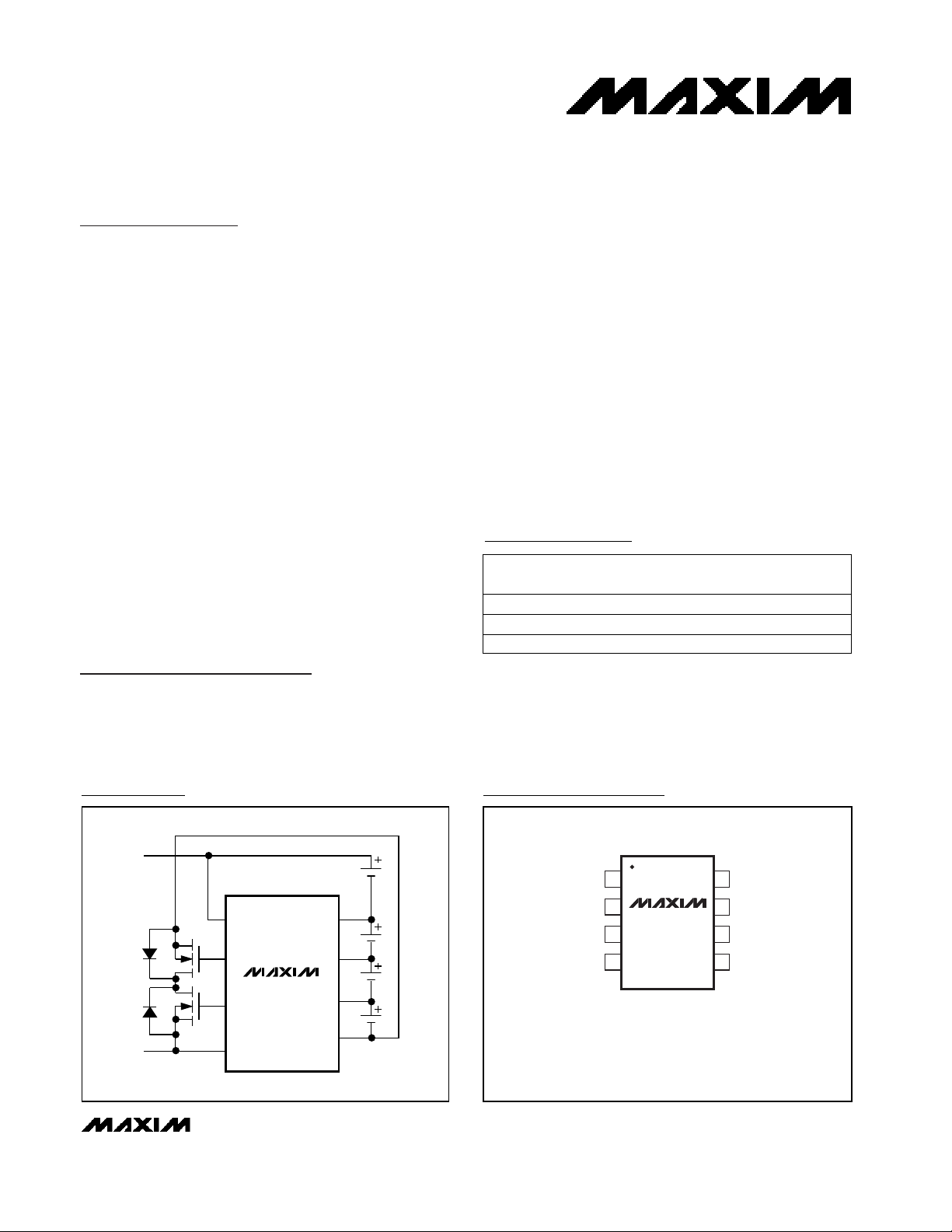
B1P
PKN
BN
1
2
87I.C. [B3P]
B2PDSG
CHG
I.C. (B4P)
NOTES: I.C. = INTERNAL CONNECTION. MAKE NO CONNECTIONS TO THIS PIN.
( ) ARE FOR THE MAX1665X.
[ ] ARE FOR THE MAX1665V AND MAX1665X.
SO
TOP VIEW
3
4
6
5
MAX1665S
MAX1665V
MAX1665X
MAX1665X
B4P B3P
DSG
B2P
B1P
PKN
(-)
(+)
CHG
BN
Typical Operating Circuit
19-1605; Rev 0; 1/00
Pin Configuration
Ordering Information
PART
MAX1665SESA
MAX1665VESA
MAX1665XESA -40°C to +85°C
-40°C to +85°C
-40°C to +85°C
TEMP. RANGE
PIN-
PACKAGE
8 SO
8 SO
8 SO
CELL
COUNT
2
3
4
Page 2
MAX1665S/V/X
Lithium-Ion Battery Pack Protector
2 _______________________________________________________________________________________
ABSOLUTE MAXIMUM RATINGS
ELECTRICAL CHARACTERISTICS
(V
B2P
= 8V (MAX1665S), V
B3P
= 12V (MAX1665V), V
B4P
= 16V (MAX1665X), TA= 0°C to +85°C, unless otherwise noted. Typical
values are at T
A
= +25°C.)
Stresses beyond those listed under “Absolute Maximum Ratings” may cause permanent damage to the device. These are stress ratings only, and functional
operation of the device at these or any other conditions beyond those indicated in the operational sections of the specifications is not implied. Exposure to
absolute maximum rating conditions for extended periods may affect device reliability.
B4P to PKN (MAX1665X)........................................-0.3V to +24V
B3P to PKN (MAX1665V)........................................-0.3V to +18V
B2P to PKN (MAX1665S)........................................-0.3V to +12V
B1P to PKN, B2P to B1P, B3P to B2P, B4P to B3P...-0.3V to +6V
CHG to PKN, DSG to BN
MAX1665S............................................-0.3V to (V
B2P
+ 0.3V)
MAX1665V............................................-0.3V to (V
B3P
+ 0.3V)
MAX1665X............................................-0.3V to (V
B4P
+ 0.3V)
B2P to BN (MAX1665S)..........................................-0.3V to +12V
B3P to BN (MAX1665V)..........................................-0.3V to +18V
B4P to BN (MAX1665X)..........................................-0.3V to +24V
Continuous Power Dissipation (T
A
= +70°C)
8-Pin SO (derate 5.88mW/°C above +70°C)...............471mW
Operating Temperature Range ...........................-40°C to +85°C
Junction Temperature......................................................+150°C
Temperature Range...........................................-65°C to +150°C
Lead Temperature (soldering, 10s) .................................+300°C
MAX1665SESA, V
B1P
= 4V nA
310
MAX1665X
MAX1665V
MAX1665S
V
PKN
= ±300mV
V
PKN
= ±300mV
(Note 1)
V
CHG
= V
PKN
+ 3.0V
CHG = PKN, DSG = BN
Cell voltage rising
I
DSG
= -1µA
VBN- V
PKN
MAX1665X, I
OUT
= 100µA, V
B4P
= 24V,
VBN= 100mV
CONDITIONS
I
BIAS
Input Bias Current (Note 3)
MAX1665VESA, V
B1P
= 4V, V
B2P
= 8V
nA
310
MAX1665XESA, V
B1P
= 4V, V
B2P
= 8V,
V
B3P
= 12V
310
ms
135
t
OFF
Overcurrent Sampling - t
OFF
ms
8.2
t
ON
Overcurrent Sampling - t
ON
mA
0.5 2
I
OL
CHG Output Sink Current
mA
10 25
I
OH
CHG, DSG Output Source
Current
V
VBN+ 0.1
V
DSGL
DSG Output Voltage Low
V
17 20
DSG Output Voltage High
(Note 2)
V
420
V
B4P
B4P Voltage Range
V
4 15
V
B3P
V
410
V
B2P
B2P Voltage Range
B3P Voltage Range
ms
10
t
IO
Overcurrent Detection Delay
ms
200
t
UV
Overvoltage/Undervoltage
Delay
mV
5
V
CH2
Overcurrent Hysteresis
mV
±200 ±250 ±300
V
CH
Overcurrent Sense Threshold
V
4.26 4.3 4.34
V
OV
Overvoltage Threshold
V
0.10
V
CE
Overvoltage Hysteresis
V
2.4 2.5 2.6
V
UV
Undervoltage Threshold
mV
0 18 30
V
RE
Undervoltage RESET
UNITSMIN TYP MAXSYMBOLPARAMETER
I
OUT
= 100µA V
V
B2P
- 1.8 V
B2P
- 0.54
CHG, DSG Output Voltage High
I
CHG
= -100µA V
V
B3P
- 1.8 V
B3P
- 0.54
MAX1665S
MAX1665V
V
PKN
+ 0.1
V
CHGL
V
B4P
- 1.8 V
B4P
- 0.54
MAX1665X
CHG Output Voltage Low
V
DSG
= V
BN
+ 3.0V µA
0.5 2
I
OL
DSG Output Sink Current
Page 3
MAX1665S/V/X
Lithium-Ion Battery Pack Protector
_______________________________________________________________________________________ 3
ELECTRICAL CHARACTERISTICS (continued)
(V
B2P
= 8V (MAX1665S), V
B3P
= 12V (MAX1665V), V
B4P
= 16V (MAX1665X), TA= 0°C to +85°C, unless otherwise noted. Typical
values are at T
A
= +25°C.)
ELECTRICAL CHARACTERISTICS
(V
B2P
= 8V (MAX1665S), V
B3P
= 12V (MAX1665V), V
B4P
= 16V (MAX1665X), TA= -40°C to +85°C, unless otherwise noted.) (Note 6)
Note 1: Applies to the differential voltage measured on any cell.
Note 2: DSG is internally clamped to a maximum of 20V to protect the external MOSFET (V
GS
).
Note 3: Guaranteed by design.
Note 4: The input bias matching between cells is measured with a 4V voltage between cells.
Note 5: At least one cell is <V
UV
.
Note 6: Specifications to -40°C are guaranteed by design, not production tested.
MAX1665SESA, V
B1P
= 4V
nA
10
MAX1665X
DSG = CHG = low
MAX1665V
MAX1665S
V
DSG
= VBN+ 0.3V
V
CHG
= V
PKN
+ 0.3V
CHG = PKN, DSG = BN
Cell voltage rising
I
DSG
= -1µA
VBN- V
PKN
MAX1665X, I
OUT
= 100µA, V
B4P
= 24V,
VBN= 100mV
CONDITIONS
I
BIAS
Input Bias Current (Note 3)
MAX1665VESA, V
B1P
= 4V, V
B2P
= 8V
10
MAX1665XESA, V
B1P
= 4V, V
B2P
= 8V,
V
B3P
= 12V
10
V
4.7
V
UVLO
Undervoltage Lockout
µA
30
I
CC
Supply Current
µA
0.2
I
OL
DSG Output Sink Current
mA
0.2
I
OL
CHG Output Sink Current
mA
10
I
OH
CHG, DSG Output Source
Current
V
VBN+ 0.1
V
DSGL
DSG Output Voltage Low
V
20
DSG Output Voltage High
(Note 2)
V
420
V
B4P
B4P Voltage Range
V
4 15
V
B3P
V
410
V
B2P
B2P Voltage Range
B3P Voltage Range
mV
±180 ±320
V
CH
Overcurrent Sense Threshold
V
4.20 4.24
V
OV
Overvoltage Threshold
V
2.4 2.6
V
UV
Undervoltage Threshold
mV
0 30
V
RE
Undervoltage RESET
UNITSMIN TYP MAXSYMBOLPARAMETER
I
OUT
= 100µA V
V
B2P
- 2 V
B2P
- 0.5
CHG, DSG Output Voltage High
I
CHG
= -100µA V
V
B3P
- 2 V
B3P
- 0.5
MAX1665S
MAX1665V
V
PKN
+ 0.1
V
CHGL
V
B4P
- 2 V
B4P
- 0.5
MAX1665X
CHG Output Voltage Low
(Note 5) µA
2
I
LP
Standby Mode Current
DSG = CHG = low
(Note 5)
CONDITIONS
(Notes 3, 4) pA
±500
∆I
BIAS
V
4.0 4.7
V
UVLO
Undervoltage Lockout
µA
0.7 1
I
LP
Standby Mode Current
µA
16 25
I
CC
Supply Current
UNITSMIN TYP MAXSYMBOLPARAMETER
Input Bias Current Matching
Page 4
MAX1665S/V/X
Lithium-Ion Battery Pack Protector
4 _______________________________________________________________________________________
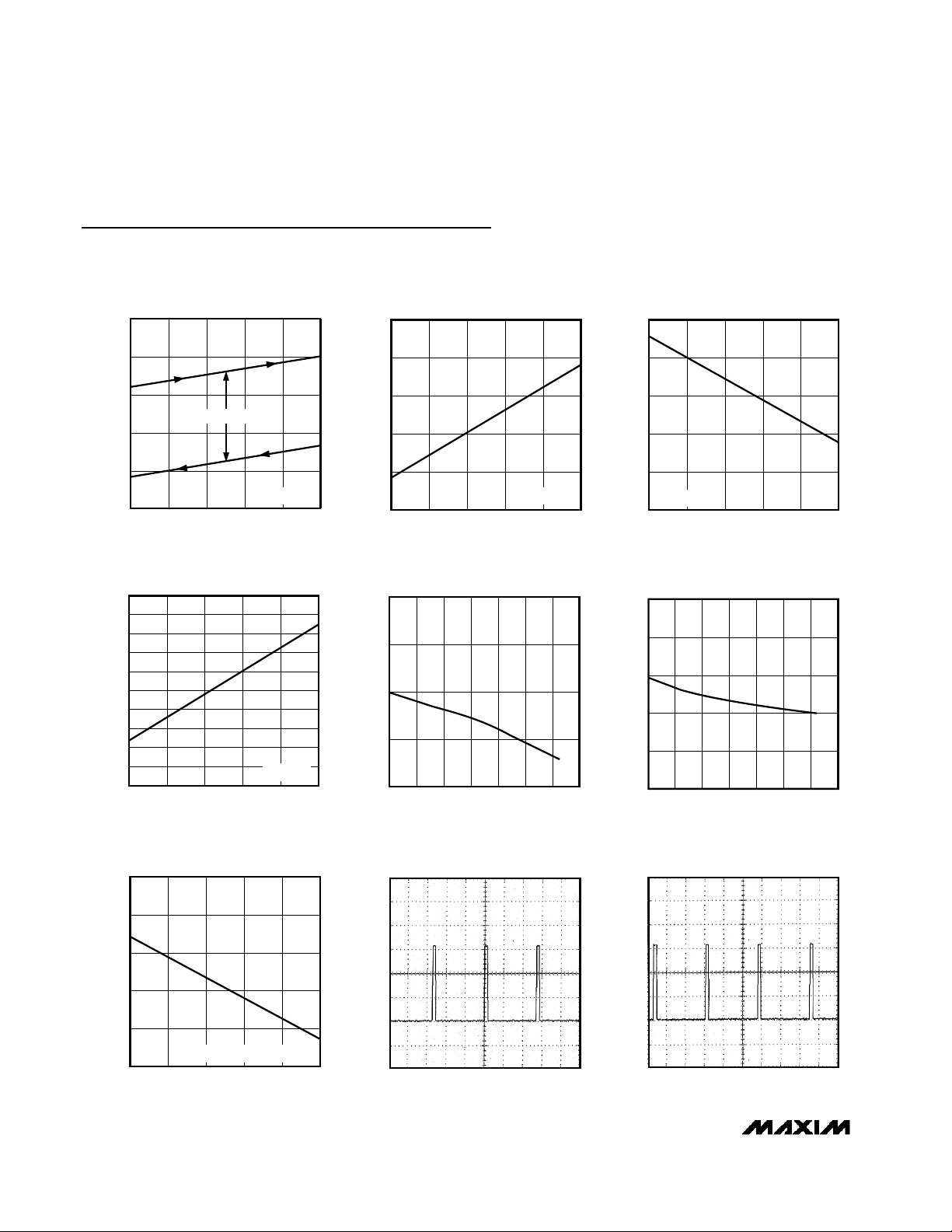
Typical Operating Characteristics
(TA = +25°C, unless otherwise noted.)
4.14
4.18
4.26
4.22
4.30
4.34
-40 10-15 35 60 85
OVERVOLTAGE THRESHOLD vs.
TEMPERATURE
MAX1665 toc01
TEMPERATURE (°C)
THRESHOLD VOLTAGE (V)
VBN
- V
PKN
HYSTERESIS
2.46
2.47
2.49
2.48
2.50
2.51
-40 10-15 35 60 85
UNDERVOLTAGE THRESHOLD vs.
TEMPERATURE
MAX1665 toc02
TEMPERATURE (°C)
UNDERVOLTAGE THRESHOLD (V)
V
BN
- V
PKN
240
243
249
246
252
255
-40 10-15 35 60 85
OVERCURRENT THRESHOLD vs.
TEMPERATURE
MAX1665 toc03
TEMPERATURE (°C)
OVERCURRENT THRESHOLD (mV)
VBN - V
PKN
-260
-254
-256
-258
-252
-250
-248
-246
-244
-242
-240
-40 10-15 35 60 85
OVERDISCHARGE THRESHOLD
vs. TEMPERATURE
MAX1665 toc04
TEMPERATURE (°C)
OVERDISCHARGE THRESHOLD (mV)
V
BN - VPKN
16.0
16.4
17.2
16.8
17.6
18.0
2.5 3.53.0 4.0 4.5 5.0
QUIESCENT CURRENT
vs. SUPPLY VOLTAGE
MAX1665 toc07
SUPPLY VOLTAGE PER CELL (V)
QUIESCENT CURRENT (µA)
NORMALIZED TO ONE CELL
16.0
16.5
17.0
17.5
18.0
SUPPLY CURRENT
vs. TEMPERATURE
MAX1665 toc05
TEMPERATURE (°C)
SUPPLY CURRENT (µA)
-40 20 40-20 0 60 80 100
0.5
0.6
0.8
0.7
0.9
1.0
-40 0-20 20 40 60 80 100
STANDBY MODE CURRENT
vs. TEMPERATURE
MAX1665 toc06
TEMPERATURE (°C)
STANDBY CURRENT (µA)
CHG
2V/div
50ms/div
CONTINUOUS OVERCHARGE CONDITION
MAX1665 toc08
DSG
2V/div
50ms/div
CONTINUOUS OVERDISCHARGE CONDITION
MAX1665 toc09
Page 5

MAX1665S/V/X
Lithium-Ion Battery Pack Protector
_______________________________________________________________________________________ 5
FUNCTION
1, 8 1 Internally Connected. Make no connection to this pin.
— —
Cell 4 Positive Input. Connect to the positive terminal of the fourth
series Li+ cell.
2 2
Discharge Control Output. Drives the gate of an external N-channel
MOSFET to control the discharge path.
3 3
Charge Control Output. Drives the gate of an external N-channel
MOSFET to control the charge path.
7 7
Cell 2 Positive Input. Connect to the positive terminal of the second
series Li+ cell.
6 6
Cell 1 Positive Input. Connect to the positive terminal of the first
series Li+ cell.
5 5 Connect to the negative terminal of the first series Li+ cell.
4 4 Pack Negative Input
— 8
Cell 3 Positive Input. Connect to the positive terminal of the third
series Li+ cell.
Pin Description
—
1
2
3
7
6
5
4
8
NAME
I.C.
B4P
DSG
CHG
B2P
B1P
BN
PKN
B3P
MAX1665VMAX1665S MAX1665X
PIN
Table 1. Functionality Truth Table for VBN< V
PKN
+ 0.018V (Discharge Mode)
*Assuming no load on CHG or DSG.
0
1
1
1 1
25Yes
NoLow
Gated
Low
Low1
10
0
1
0
1
1
0
0 1
25
1No
Yes
NoLow
Gated
Low
Low
Gated
Low0
1
10
0
0
UNDERVOLTAGE
0
1
0
OVERVOLTAGE
0
0
1 25
1
25
MAX
SUPPLY
CURRENT*
(µA)
GATE
CLOCKED
No
No
NoHigh
Low
High
DSG
Low
Low
High
CHG
DISCHARGE
OVERCURRENT
0
0
00
0
0
CHARGE
OVERCURRENT
Page 6

MAX1665S/V/X
Lithium-Ion Battery Pack Protector
6 _______________________________________________________________________________________
Figure 1. State Diagram
_______________Detailed Description
The MAX1665S, MAX1665V, and MAX1665X supervise
the charging and discharging processes on Li+ cells.
Designed for 2, 3, and 4-cell applications, these devices
monitor the voltage across each cell to provide protection against overcurrent, overvoltage, and undervoltage.
Figure 1 shows the MAX1665 state diagram. Two control pins, CHG and DSG, drive the gates of two seriesconnected external N-channel MOSFETs, enabling/
disabling the charging/discharging process as necessary (see Typical Operating Circuit). The voltages at
B1P, B2P, B3P, and B4P are measured differentially
Table 2. Functionality Truth Table for VBN> V
PKN
+ 0.018V (Charge Mode)
*Assuming no load on CHG or DSG.
0
1
1
1 25
25No
NoHigh
High
Low
Low0
01
1
1
0
1
1
0
0 25
25
25No
Yes
YesGated
Gated
High
Gated
Gated
Low0
0
01
1
0
UNDERVOLTAGE
0
1
0
OVERVOLTAGE
0
0
1 25
25
25
MAX
SUPPLY
CURRENT*
(µA)
GATE
CLOCKED
No
No
NoHigh
High
High
DSG
Low
High
High
CHG
DISCHARGE
OVERCURRENT
0
0
00
0
0
CHARGE
OVERCURRENT
POWER
ON
POWER
SLEEP
DSG = 0
ON
CHG = 0
CHARGE = 0
NORMAL
DSG = 1
CHG = 1
SUPPLIES
ON
DSG = 0
CHG = 0
∆T =
2.4ms
CHARGE = 1 RDY = 1
UV = 0
OV = 0
NORMAL
PULSE OFF
DSG = *
CHG = *
START
COUNTER
DSG = 0
CHG = 0
∆T =
96ms
∆T =
2.4ms
NORMAL
PULSE ON
DSG = 1
CHG = 1
START-UP
ZCHK
DSG = 0
CHG = 0
∆T =
6.4ms
∆T =
160µs
NORMAL
ZCHK
DSG = 1
CHG = 1
START-UP
MEASURE
DSG = 0
CHG = 0
∆T =
160µs
∆T =
640µs
SHORT = 1 SHORT = 1
WAIT FOR
BLANK = 0
DSG = 0
CHG = 0
NORMAL
MEASURE
DSG = 1
CHG = 1
∆T =
2.4ms
∆T =
640µs
UV = 0
OV = 1
UV = 1
OV = 0
UV = 1
OV = 1
* = 0 FOR OVERCURRENT FAULT; 1 OTHERWISE
OV
DSG = 1
CHG = 0
DSG = 1
CHG = 1
OV & UV
DSG = 1
CHG = 0
∆T =
2.4ms
UV
∆T =
2.4ms
CHARGE = 0 CHARGE = 0 CHARGE = 0 CHARGE = 0
∆T =
2.4ms
OV
PULSE OFF
DSG = 1
CHG = 0
UV
PULSE OFF
DSG = *
CHG = *
OV & UV
PULSE OFF
DSG = 1
CHG = 0
∆T =
96ms
∆T =
96ms
∆T =
96ms
OV
PULSE ON
DSG = 1
CHG = 0
UV
PULSE ON
DSG = 1
CHG = 1
OV & UV
PULSE ON
DSG = 1
CHG = 0
∆T =
6.4ms
∆T =
6.4ms
∆T =
6.4ms
OV
ZCHK
DSG = 1
CHG = 0
UV
ZCHK
DSG = 1
CHG = 1
OV & UV
ZCHK
DSG = 1
CHG = 0
∆T =
160µs
∆T =
160µs
∆T = 160µs
OV
MEASURE
DSG = 1
CHG = 0
SHORT = 1
UV
MEASURE
DSG = 1
CHG = 1
SHORT = 1
OV & UV
MEASURE
DSG = 1
CHG = 0
∆T =
640µs
∆T =
640µs
∆T =
640µs
Page 7

MAX1665S/V/X
Lithium-Ion Battery Pack Protector
_______________________________________________________________________________________ 7
across each cell to determine if the voltage levels are
within operating range.
As depicted in the typical operating circuit, when CHG
and DSG are high, the MOSFETs are on, allowing the
cells to charge or discharge. However, when the
charge or discharge current becomes excessive, the
device turns off the FETs, enters a standby mode, and
periodically samples the current to determine if the fault
condition is removed. The MAX1665 does not sample
the current directly, but rather measures the differential
voltage across BN and PKN produced by the charge or
discharge current flowing through the drain-to-source
resistance of the MOSFETs. A preset voltage threshold
is used to prevent excess current flow (see Electrical
Characteristics).
In operating mode, all of the MAX1665 versions consume less than 25µA of quiescent current, allowing
long-term battery storage without significantly affecting
battery life. In standby mode, these devices consume
less than 1µA of quiescent current.
Overvoltage Protection
When any individual cell voltage rises above VOV(overvoltage limit), the charge MOSFET control pin (CHG) is
driven to PKN, thereby disconnecting the charger from
the cells. The MAX1665 measures each cell of the pack
differentially to prevent overcharging on a cell-by-cell
basis. The charging process resumes when the highest
cell voltage drops below VOV- 100mV (see Typical
Operating Circuit).
Undervoltage/Overdischarge Protection
Discharge can occur whenever the voltage of each cell
is above the undervoltage threshold voltage (VUV, typically 2.50V). If the voltage on any of the cells falls
below VUV, CHG latches to PKN and DSG latches to
BN. Quiescent current falls to under 1µA as the device
enters the standby mode. The latch resets when BN
exceeds PKN by 18mV.
During charge mode, when BN is greater than PKN, the
latch is held in reset, which disables the undervoltage
comparator feature and allows charging on the cells.
During the initialization process, as cells are connected
to the MAX1665, the device considers this a low-voltage condition and disables CHG and DSG until a
charging source is applied to create at least an 18mV
differential between BN and PKN.
During long-term storage, the battery will self-discharge until it reaches the undervoltage threshold.
When this happens, the MAX1665 enters standby
mode. Normal operating mode resumes when a charger is connected, causing BN to rise 18mV above PKN.
Overcurrent Protection
When the MAX1665 detects overcurrent in the system,
it disables the charge or discharge process by connecting CHG to PKN and DSG to BN, turning off the
external MOSFETs (see Typical Operating Circuit). In
charge mode, the MAX1665 detects overcharge when
the voltage from BN to PKN exceeds +250mV. In discharge mode, overdischarge occurs when the differential voltage is less than -250mV. During any overcurrent
condition, CHG and DSG are gated at 12Hz until the
overcurrent is removed.
If both an overvoltage and overcharge condition exist,
the overvoltage condition takes priority. Likewise, if
undervoltage and overdischarge conditions exist, the
overdischarge condition takes priority. For more
details, see Tables 1 and 2.
Cell Current Balancing
When the battery cells are matched, the MAX1665
draws zero current from the intermediate nodes. The
MAX1665 draws current from the top terminal only.
Figure 2 shows a simplified diagram of the voltage
sampling scheme. The following equations show that,
for balanced cells, the differential discharge currents
are zero:
B4P: I4= 3ICB+ V4/ R = 4V4/ R = BAT4 current
B3P: I3= I3P+ I4= BAT3 current
I3P+ ICB= V3/ R ⇒ I3P= V3/ R - V4/ R
I3= I4+ (V3- V4) / R = (3V4+ V3) / R
B2P: I2= I2P+ I3= BAT2 current
I2P+ ICB= V2/ R ⇒ I2P= V2/ R - V4/ R
I2= I3 + V2/ R - V4/ R = I4+ (V3- V4) / R +
(V2- V4) / R = (2V4+ V3+ V2) / R
B1P: I1= I1P+ I2= BAT1 current
I1P+ ICB= V1 / R ⇒ I1P= V1/ R - V4/ R
I1= I2+ V1/ R - V4/ R = I4+ (V3- V4) / R +
(V2- V4) / R + (V1- V4) / R
= (V4+ V3+ V2+ V1) / R
when V1= V2= V3= V4, I1P= I2P= I3P= 0 and I1=
I2= I3= I4= 4V4/ R.
Due to process variations, the MAX1665 does draw a
minute current (70nA ~ 150nA) from the intermediate
node even when the cells are matched. This current
difference exists in the sampling mode, which is 1/32 of
the whole time period, making the average of this current 2nA to 5nA.
Page 8

MAX1665S/V/X
Lithium-Ion Battery Pack Protector
8 _______________________________________________________________________________________
Applications Information
Choosing an External MOSFET
The external N-channel MOSFETs act as gated switches to enable or disable the charging/discharging
process. CHG and DSG control the gate of these external MOSFETs to prevent damage to the
Li+ cells. For
overcurrent conditions, the voltage at DSG equals the
voltage at BN, thereby reducing all current flow, including the path through the body diode of the
N-channel MOSFET. Note that the MAX1665X clamps
the V
GS
voltage to a maximum of 20V.
The IRF7101 is a low-cost, dual N-channel MOSFET
that is available in a small 8-pin SO package.
Depending on the maximum charge and discharge
rates, use different MOSFETs to optimize each application. Table 3 summarizes recommended MOSFETs.
2, 3, and 4-Cell Applications
Figures 3 through 5 depict circuits for 2, 3, and 4-cell
applications. Note that the two series MOSFETs (IRF7101
dual N-channel MOSFETs) are oriented to prevent body
diode current flow. The indicated polarity symbols show
the connection for the external source required to charge
the Li+ cells. This external charger source also supplies
the gate drive to the MOSFETs through pack + voltage /
pack.
DUAL N-CHANNEL
MOSFETs
IRF9956
FDS6990A
Si9936 0.050
0.018
0.10
TYPICAL
R
DS(ON)
(Ω)
±20
±20
±20
MAX V
GS
(V)
Table 3. Recommended MOSFETs
Figure 2. Sampling Mode Equivalent Circuit
Figure 3. Typical 2-Cell Operating Circuit
BP4
I
BP3
I
3
BP2
I
2
BP1
I
1
4
I
3P
I
2P
I
+
1P
V
1
B1P1
R
V
4
I
CB
+
R
V
2
V
1
R
B2P1
V
4
I
CB
R
+
V
3
V
2
R
B3P1
V
4
I
CB
R
+
V
4
V
3
R
+
V
4
+
V
3
+
V
2
+
V
1
RRR
V
4
R
PACK+
OVERDISCHARGE
PROTECTION
OVERCHARGE
PROTECTION
PACK-
CELL 2
CELL 1
IRF7101
IRF7101
1
8
7
6
5
2
3
4
I.C.
I.C.
B2P
B1P
BN
DSG
CHG
PKN
MAX1665S
Page 9

MAX1665S/V/X
Lithium-Ion Battery Pack Protector
_______________________________________________________________________________________ 9
PACK+
Figure 4. Typical 3-Cell Operating Circuit
Figure 5. Typical 4-Cell Operating Circuit
OVERDISCHARGE
PROTECTION
OVERCHARGE
PROTECTION
CELL 3
CELL 2
CELL 1
IRF7101
IRF7101
1
I.C.
8
B3P
7
B2P
6
B1P
5
MAX1665V
BN
2
DSG
3
CHG
PACK+
CELL 4
CELL 3
CELL 2
CELL 1
OVERDISCHARGE
PROTECTION
OVERCHARGE
PROTECTION
IRF7101
IRF7101
1
B4P
8
B3P
7
B2P
6
B1P
5
MAX1665X
BN
2
DSG
3
CHG
PACK-
4
PKN
PACK-
4
PKN
Page 10

MAX1665S/V/X
Lithium-Ion Battery Pack Protector
10 ______________________________________________________________________________________
________________________________________________________Package Information
Page 11

MAX1665S/V/X
Lithium-Ion Battery Pack Protector
______________________________________________________________________________________ 11
NOTES
Page 12

MAX1665S/V/X
Lithium-Ion Battery Pack Protector
Maxim cannot assume responsibility for use of any circuitry other than circuitry entirely embodied in a Maxim product. No circuit patent licenses are
implied. Maxim reserves the right to change the circuitry and specifications without notice at any time.
12 ____________________Maxim Integrated Products, 120 San Gabriel Drive, Sunnyvale, CA 94086 408-737-7600
© 2000 Maxim Integrated Products Printed USA is a registered trademark of Maxim Integrated Products.
NOTES
 Loading...