

Page 1
General Description
The MAX1660 digitally controlled fuel-gauge interface
executes two essential functions for rechargeable battery-pack management: fuel gauging and pack overcurrent protection. It accurately monitors a battery pack’s
charge and discharge current flow, and records each
using two independent, on-board Coulomb counters.
Each counter’s contents are externally accessible via a
System Management Bus (SMBus™)-compatible 2-wire
serial interface. An optional third wire interrupts the
microcontroller (µC) when the charge or discharge
counters reach a preset value, or when an overcurrent
condition (charge or discharge) occurs. In the event of
an overcurrent or short-circuit condition, the MAX1660
disconnects the load and alerts its host. The MAX1660’s
flexibility allows accurate fuel gauging for any battery
chemistry, using any desired control algorithm.
The MAX1660 operates with battery voltages from +4V
to +28V and provides two micropower shutdown
modes, increasing battery lifetime. To minimize total
parts count, the device integrates a precision 2.00V
system-reference output, a 3.3V linear-regulator output
that can supply up to 5mA to power external circuitry,
and a power-on reset output for the system µC. The
MAX1660 is available in a 16-pin QSOP package.
________________________Applications
Smart-Battery Packs Battery-Pack Fuel Gauging
Battery-Pack Overcurrent Digital Current-Sense
Protection Instrumentation
Industrial-Control System Analog-to-Digital
Interfaces Conversion
____________________________Features
♦ 1% Accuracy over a 600µA to 4A Current Range
(R
SENSE
= 30mΩ)
♦ 5µV Input Offset Voltage (28µV max)
♦ SMBus 2-Wire (plus optional interrupt)
Serial Interface
♦ 2.00V Precision System Reference Output
♦ 3.3V Linear-Regulator Output Powers External
Circuitry
♦ Two Micropower Shutdown Modes
♦ Independent 32-Bit Charge and Discharge
Coulomb Counters
♦ Battery-Overcharge/Overdischarge Protection
♦ Battery Short-Circuit/Overcurrent Protection
♦ On-Board Power MOSFET Drivers
♦ 80µA Quiescent Current
♦ <1µA Shutdown Current
♦ Small 16-Pin QSOP Package
(same board area as 8-pin SO)
MAX1660
*
Digitally Controlled
Fuel-Gauge Interface
________________________________________________________________
Maxim Integrated Products
1
19-1308; Rev 1; 10/98
EVALUATION KIT MANUAL
FOLLOWS DATA SHEET
SMBus is a trademark of Intel Corp.
*
Patent pending
MAX1660
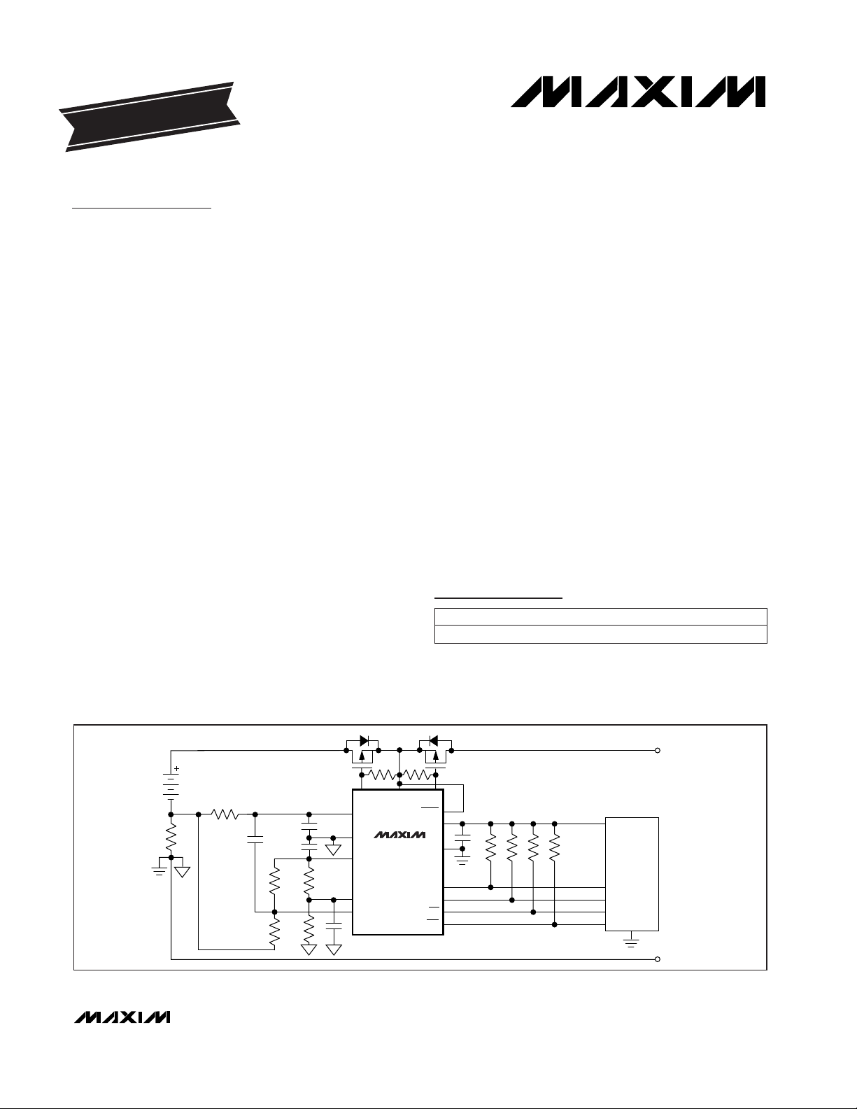
BATT
CS
AGND
REF
OCI
ODI
GND
SCL
SDA
SHDN
OCO
VL
V
CC
GND
PACK-
PACK+
µC
RST
INT
ODO
R
CS
___________________________________________________Typical Operating Circuit
For free samples & the latest literature: http://www.maxim-ic.com, or phone 1-800-998-8800.
For small orders, phone 1-800-835-8769.
PART
MAX1660EEE -40°C to +85°C
TEMP. RANGE PIN-PACKAGE
16 QSOP
Ordering Information
Pin Configuration appears at end of data sheet.
Page 2
*
Patent pending
MAX1660
*
Digitally Controlled
Fuel-Gauge Interface
2 _______________________________________________________________________________________
ABSOLUTE MAXIMUM RATINGS
ELECTRICAL CHARACTERISTICS
(V
SHDN
= V
BATT
= 12V, V
SCL
= V
SDA
= 3.6V, C
REF
= 10nF, CVL= 0.1µF, TA= 0°C to +85°C, unless otherwise noted. Typical values
are at T
A
= +25°C.)
Stresses beyond those listed under “Absolute Maximum Ratings” may cause permanent damage to the device. These are stress ratings only, and functional
operation of the device at these or any other conditions beyond those indicated in the operational sections of the specifications is not implied. Exposure to
absolute maximum rating conditions for extended periods may affect device reliability.
BATT, ODO, OCO, SHDN to GND .........................-0.3V to +30V
SCL, SDA, INT, RST to GND ....................................-0.3V to +6V
REF, ODI, OCI to GND..................................-0.3V to (VL + 0.3V)
VL to GND ................................................................-0.3V to +6V
CS to GND...................................................................-2V to +6V
AGND to GND.............................................................-1V to +1V
Continuous Power Dissipation (T
A
= +70°C)
16-Pin QSOP (derate 8.3mW/°C above +70°C).............667mW
Operating Temperature Range ...........................-40°C to +85°C
Storage Temperature Range.............................-65°C to +165°C
Lead Temperature (soldering, 10sec).............................+300°C
V
OCO
= 0.4V
V
ODO
= 28V
V
SHDN
= 3.3V, SOFTSHDN = 0, IVL= 0
V
ODO
= 0.4V
(Note 1)
VCS= 120mV
VCS= 0
0 ≤ I
REF
≤ 200µA
I
REF
= 0
V
SHDN
= 3.3V, SOFTSHDN = 1, IVL= 0
V
SHDN
≤ 0.4V
SOFTSHDN = 0, 0 ≤ IVL≤ 5mA
VCS= -120mV
SOFTSHDN = 1, 0 ≤ IVL≤ 5mA
VCS= 0
CONDITIONS
mA1 2.5OCO Sink Current
µA0.01 1ODO Off-Leakage Current
mA1 2.5ODO Sink Current
µs1Propagation Delay
µA-1 0.01 1OCI, ODI Input Offset Current
mV-7 0 7OCI, ODI Input Offset Voltage
49,500 50,000 50,500
counts/
sec
0212
Charge Coulomb-Counter
Accumulation Rate
49,500 50,000 50,500
counts/
sec
0212
Discharge Coulomb-Counter
Accumulation Rate
µA
80 135
I
BATT
BATT Supply Current
V428V
BATT
BATT Input Voltage Range
kΩ100CS to AGND Input Resistance
µV/µA10 50REF Load Regulation
V1.96 2.00 2.04V
REF
REF Output Voltage
15 30
0.02 1
V
3.1 3.25 3.4
V
VL
VL Output Voltage
3.1 3.25 3.6
UNITSMIN TYP MAXSYMBOLPARAMETER
V
INT
= 0.4V
V
SDA
= 0.6V
SHDN
SCL, SDA
SHDN, SCL, SDA
V
OCO
= 28V
mA2V
OL
INT Output Low Sink Current
mA6V
OL
SDA Output Low Sink Current
0.6
V
0.8
V
IL
Input Low Voltage
V2.2V
IH
Input High Voltage
µA0.01 1OCO Off-Leakage Current
SUPPLY AND REFERENCES
FUEL GAUGE
OVERCURRENT COMPARATOR
INTERFACE-LOGIC LEVELS
Page 3
MAX1660
*
Digitally Controlled
Fuel-Gauge Interface
_______________________________________________________________________________________ 3
ELECTRICAL CHARACTERISTICS (continued)
(V
SHDN
= V
BATT
= 12V, V
SCL
= V
SDA
= 3.6V, C
REF
= 10nF, CVL= 0.1µF, TA= 0°C to +85°C, unless otherwise noted. Typical values
are at T
A
= +25°C.)
V
TH1
, VL rising
VVL= 3V, I
SINK
= 1.2mA
CONDITIONS
VVL= 1V, I
SINK
= 50µA
V
TH2
, VL falling
2.75 2.90 3.05
V
1.0 1.7 2.2
0.3
V
0.3
V
RST
RST Output Voltage
V
TH1
,
V
TH2
RST Threshold Voltage
UNITSMIN TYP MAXSYMBOLPARAMETER
SHDN forced to 28V
SHDN forced to 3.6V
Output forced to 5V
ms25
RST Active Timeout Period
20 100
µA
0.7 3.0
I
SHDN
SHDN Input Bias Current
µA0.01 1
SCL, SDA, INT, RST Leakage
Current
V
ODO
= 0.4V
V
ODO
= 28V
V
SHDN
= 3.3V, SOFTSHDN = 0, IVL= 0
V
ODO
= 0.4V
(Note 1)
VCS= 120mV
VCS= 0
0 ≤ I
REF
≤ 200µA
I
REF
= 0
V
SHDN
= 3.3V, SOFTSHDN = 1, IVL= 0
V
SHDN
≤ 0.4V
SOFTSHDN = 0, 0 ≤ IVL≤ 5mA
VCS= -120mV
SOFTSHDN = 1, 0 ≤ IVL≤ 5mA
VCS= 0
CONDITIONS
mA1OCO Sink Current
µA1ODO Off-Leakage Current
mA1ODO Sink Current
µA-1 1OCI, ODI Input Offset Current
mV-10 10OCI, ODI Input Offset Voltage
49,250 50,750
counts/
sec
012
Charge Coulomb-Counter
Accumulation Rate
counts/
sec
012
Discharge Coulomb-Counter
Accumulation Rate
µA
135
I
BATT
BATT Supply Current
V428V
BATT
BATT Input Voltage Range
µV/µA50REF Load Regulation
V1.96 2.04V
REF
REF Output Voltage
30
1
V
3.1 3.4
V
VL
VL Output Voltage
3.1 3.6
UNITSMIN TYP MAXSYMBOLPARAMETER
V
ODO
= 28V µA1OCO Off-Leakage Current
ELECTRICAL CHARACTERISTICS
(V
SHDN
= V
BATT
= 12V, V
SCL
= V
SDA
= 3.6V, C
REF
= 10nF, CVL= 0.1µF, TA= -40°C to +85°C, unless otherwise noted.) (Note 2)
SUPPLY AND REFERENCES
FUEL GAUGE
OVERCURRENT COMPARATOR
*
Patent pending
Page 4
*
Patent pending
MAX1660
*
Digitally Controlled
Fuel-Gauge Interface
4 _______________________________________________________________________________________
V
TH1
, VL rising
VVL= 3V, I
SINK
= 1.2mA
CONDITIONS
VVL= 1V, I
SINK
= 50µA
V
TH2
, VL falling
2.75 3.05
V
1.0 2.2
0.3
V
0.3
V
RST
RST Output Voltage
V
TH1
,
V
TH2
RST Threshold Voltage
UNITSMIN TYP MAXSYMBOLPARAMETER
SHDN forced to 28V
SHDN forced to 3.6V
Output forced to 5V
V
INT
= 0.4V
V
SDA
= 0.6V
SHDN
SCL, SDA
SHDN, SCL, SDA
120
µA
3.0
I
SHDN
SHDN Input Bias Current
µA1
SCL, SDA, INT, RST Leakage
Current
mA2V
OL
INT, RST Output Low Sink Current
mA6V
OL
SDA Output Low Sink Current
0.6
V
0.8
V
IL
Input Low Voltage
V2.2V
IH
Input High Voltage
ELECTRICAL CHARACTERISTICS (continued)
(V
SHDN
= V
BATT
= 12V, V
SCL
= V
SDA
= 3.6V, C
REF
= 10nF, CVL= 0.1µF, TA= -40°C to +85°C, unless otherwise noted.) (Note 2)
TIMING CHARACTERISTICS
(TA= 0°C to +85°C, unless otherwise noted.)
CONDITIONS
µs4.7t
SU:STA
Start-Condition Setup Time
µs4.7t
LOW
µs4t
HIGH
SCL Serial-Clock High Period
SCL Serial-Clock Low Period
µs4t
HD:STA
Start-Condition Hold Time
ns800t
SU:DAT
SDA Valid to SCL Rising-Edge Setup
Time, Slave Clocking in Data
ns0t
HD:DAT
SCL Falling Edge to SDA Transition
µs1t
DV
SCL Falling Edge to SDA Valid, Master
Clocking in Data
UNITSMIN TYP MAXSYMBOLPARAMETER
INTERFACE-LOGIC LEVELS
Page 5
MAX1660
*
Digitally Controlled
Fuel-Gauge Interface
_______________________________________________________________________________________ 5
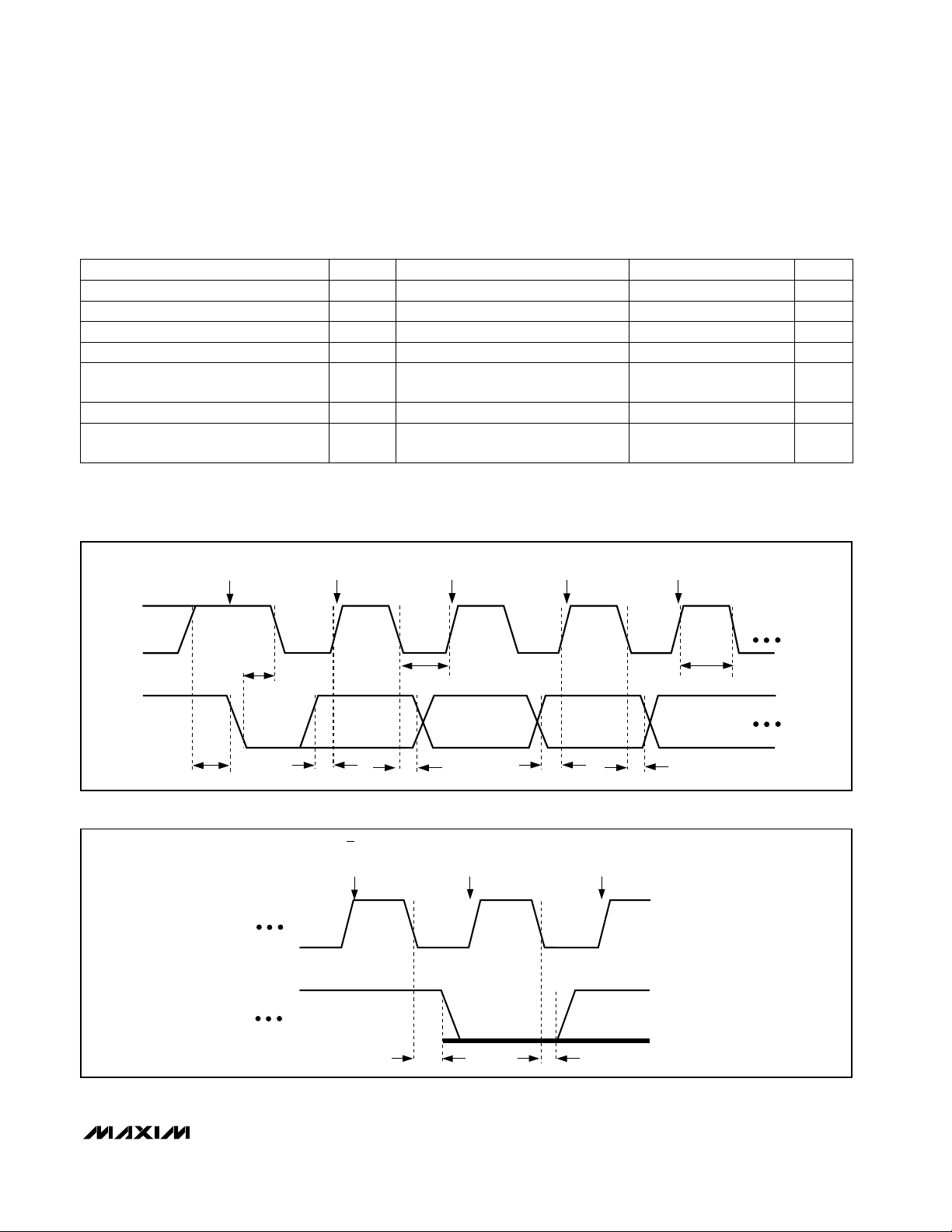
SCL
START
CONDITION
t
HIGH
SDA
t
LOW
t
HD:STA
t
SU:STA
t
SU:DAT
t
HD:DAT
t
SU:DAT
t
HD:DAT
MOST SIGNIFICANT ADDRESS BIT
(A6) CLOCKED INTO SLAVE
A5 CLOCKED
INTO SLAVE
A4 CLOCKED
INTO SLAVE
A3 CLOCKED
INTO SLAVE
Note 1: OCI and ODI are MOSFET inputs. Minimum and maximum limits are for production screening only. Actual performance is
indicated in typical value.
Note 2: Specifications to -40°C are guaranteed by design, not production tested.
CONDITIONS
µs1t
DV
SCL Falling Edge to SDA Valid, Master
Clocking in Data
ns0t
HD:DAT
SCL Falling Edge to SDA Transition
ns800t
SU:DAT
SDA Valid to SCL Rising-Edge Setup
Time, Slave Clocking in Data
µs4t
HD:STA
Start-Condition Hold Time
µs4.7t
SU:STA
Start-Condition Setup Time
µs4.7t
LOW
SCL Serial-Clock Low Period
µs4t
HIGH
SCL Serial-Clock High Period
UNITSMIN TYP MAXSYMBOLPARAMETER
TIMING CHARACTERISTICS
(TA= -40°C to +85°C, unless otherwise noted.) (Note 2)
Figure 1. SMBus Serial-Interface Timing—Address
SCL
RW BIT
CLOCKED
INTO SLAVE
SDA
t
DV
t
DV
ACKNOWLEDGE
BIT CLOCKED
INTO MASTER
SLAVE PULLING
SDA LOW
MOST SIGNIFICANT BIT
OF DATA CLOCKED
INTO MASTER
Figure 2. SMBus Serial-Interface Timing—Acknowledge
*
Patent pending
Page 6
*
Patent pending
MAX1660
*
Digitally Controlled
Fuel-Gauge Interface
6 _______________________________________________________________________________________
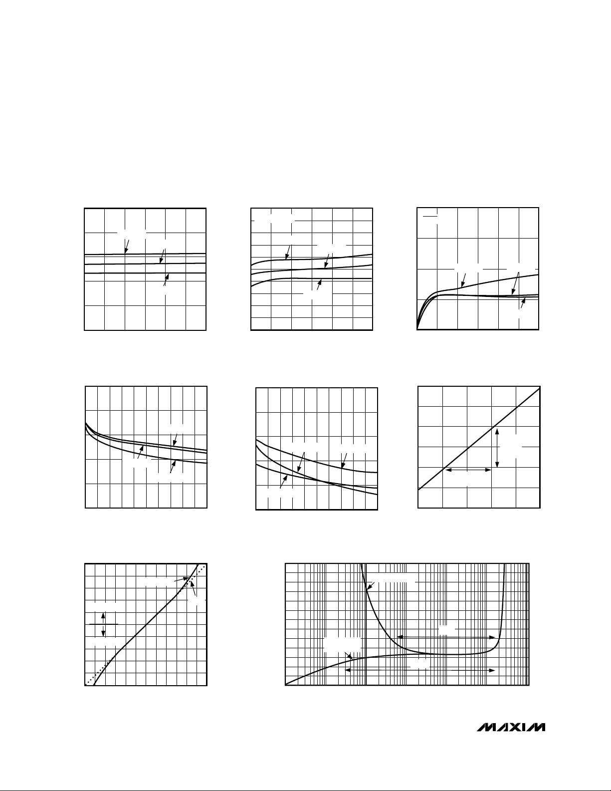
__________________________________________Typical Operating Characteristics
(V
BATT
= V
SHDN
= 12V, C
REF
= 10nF, CVL= 0.1µF, TA= +25°C, unless otherwise noted.)
50
60
70
80
90
100
412816202428
SUPPLY CURRENT vs. V
BATT
MAX1660-01
V
BATT
(V)
SUPPLY CURRENT (µA)
TA = +85°C
TA = +25°C
TA = -40°C
10
12
11
14
13
16
15
18
19
17
20
412816202428
SHUTDOWN SUPPLY CURRENT
vs. V
BATT
MAX1660-02
V
BATT
(V)
SUPPLY CURRENT (µA)
SOFTSHDN = 1
TA = -40°C
TA = +25°C
TA = +85°C
0.01
0.02
0.03
0.04
0.05
412816202428
SHUTDOWN SUPPLY CURRENT
vs. V
BATT
MAX1660-03
V
BATT
(V)
SUPPLY CURRENT (µA)
TA = +25°C
TA = +85°C
SHDN = GND
T
A
= -40°C
3.15
3.18
3.21
3.24
3.27
3.30
0 1.5 2.00.5 1.0 2.5 3.0 3.5 4.0 4.5 5.0
VL VOLTAGE vs. VL LOAD CURRENT
MAX1660-04
LOAD CURRENT (mA)
VL VOLTAGE (V)
TA = +25°C
TA = +85°C
TA = -40°C
1.994
1.996
1.998
2.000
2.002
2.004
0608020 40 100 120 140 160 180 200
REFERENCE VOLTAGE
vs. REFERENCE LOAD CURRENT
MAX1660 05
LOAD CURRENT (µA)
VOLTAGE (V)
TA = +25°C
TA = +85°C
TA = -40°C
-4
-2
0
2
6
4
8
-15 -5-10 0 5 10
FREQUENCY vs. INPUT VOLTAGE
MAX1660-06
INPUT VOLTAGE (µV)
FREQUENCY (Hz)
INPUT
OFFSET
FREQUENCY
INPUT OFFSET
VOLTAGE
150
90
120
60
0
30
120
90
60
30
150
-360
-120
0
-240
120 240 360
FREQUENCY vs. INPUT VOLTAGE
MAX1660-07
INPUT VOLTAGE (mV)
FREQUENCY (kHz)
IDEAL
MEASURED
CHGCOUNT
DISCOUNT
456
404
0.001 0.01 0.1 1 10 100 1000
CONVERSION GAIN vs. INPUT VOLTAGE
416
412
408
MAX1660-08
INPUT VOLTAGE (mV)
CONVERSION GAIN (Hz/mV)
424
420
436
432
428
448
444
440
452
*SEE INTERNAL OFFSET MEASUREMENT SECTION
OFFSET
CORRECTED*
275:1
6000:1
UNCORRECTED*
Page 7

_______________Detailed Description
The MAX1660 measures the cumulative charge into
(charging) and out of (discharging) the system battery
pack and stores the information in one of two internal,
independent charge and discharge counters. It
achieves battery-pack overcharge and overdischarge
protection through a powerful digital compare function
that interrupts the host CPU when the charge or discharge counter reaches a host-programmed value. The
device also informs the host of changes in the direction
of current flow and protects the battery pack from
short-circuit and overcurrent conditions.
The MAX1660 incorporates a 2-wire System Management Bus (SMBus™)-compliant serial interface,
allowing access to charge/discharge counters and
internal registers. An optional third wire provides an
SMBALERT#-compliant interrupt signal, or it may be used
as a simple, stand-alone host interrupt.
Coulomb-Counting Interface
The MAX1660’s Coulomb-counting interface monitors
the charge flowing in either the charging or discharging
direction, and counts the Coulombs of charge by incrementing either the charge counter (CHGCOUNT) or the
discharge counter (DISCOUNT) accordingly. The number of counter increments generated per Coulomb of
charge sensed (conversion gain) is given by the following equation:
where RCSis the current-sense resistor (see the
Typical
Operating Circuit
). The gain factor is the constant of
proportionality that relates the counter values stored in
CHGCOUNT and DISCOUNT to the amount of charge
flow into or out of the battery pack. A higher conversion
gain (larger RCS) increases resolution at low currents,
A = 416.7 10 R
Counts
Coulomb
CCS
3
⋅
MAX1660
*
Digitally Controlled
Fuel-Gauge Interface
_______________________________________________________________________________________________________ 7
______________________________________________________________Pin Description
NAME FUNCTION
1
INT
Open-Drain Host-Interrupt Output. INT sinks current when active, otherwise high-impedance (see
INT
Output
section). INT is compatible with the SMBus SMBALERT# (the “#” indicates asserted low) signal.
Connect a 100kΩ pull-up resistor between INT and VL. Leave INT unconnected if host interrupt is not used.
2
SHDN
Active-Low Shutdown Input (see
Shutdown Modes
section)
PIN
3 N.C. No Connection. Not internally connected.
4 CS Current-Sense Resistor Input
8 OCI Charge Overcurrent-Detection Input (see
Overcurrent Detection
section)
7 ODI Discharge Overcurrent-Detection Input (see
Overcurrent Detection
section)
6 REF
2.00V Reference Output. Bypass REF to AGND with a 10nF capacitor (see
Internal Regulator and Reference
section).
5 AGND Analog Ground
13 OCO
High-Voltage, Open-Drain MOSFET Gate-Driver Output. OCO controls activation of the battery-charge path
(see
OCO and ODO Gate Drivers
section).
12 ODO
High-Voltage, Open-Drain MOSFET Gate-Driver Output. ODO controls activation of the battery-discharge
path (see
OCO and ODO Gate Drivers
section).
11 BATT Supply Input
10 VL
3.3V Linear-Regulator Output. Bypass VL with a 0.33µF capacitor to GND (see
Internal Regulator and
Reference
section).
9 GND Ground
16 SCL Serial-Clock Input. Connect a 10kΩ resistor between SDA and VL (see
SMBus Interface
section).
15 SDA Serial-Data Input/Output. Connect a 10kΩ resistor between SDA and VL (see
SMBus Interface
section).
14
RST
Active-Low Reset Output. Connect a 100kΩ pull-up resistor between RST and VL. Leave RST unconnected
if the power-on reset function is not used (see
RST Output
section).
*
Patent pending
Page 8

MAX1660
*
but limits the maximum measurable current. Likewise, a
smaller conversion gain (smaller RCS) decreases resolution at low currents, but increases the maximum measurable current. A 30mΩ current-sense resistor (AC=
12.5 x 10³counts per Coulomb) provides a good balance between resolution and input current range for
many applications. With this current-sense resistance,
the MAX1660 typically measures currents from 600µA to
4A with better than 1% accuracy (see the section
Choosing R
CS
).
Charge and Discharge Counters
Figure 3 shows the functional diagram of the MAX1660’s
Coulomb-counter section. The Coulomb counter’s output increments (but never decrements) one of two independent 32-bit counters: CHGCOUNT for charging
currents, and DISCOUNT for discharging currents. By
independently counting the charge and discharge currents, the MAX1660 can accommodate any algorithm to
account for a battery pack’s energy-conversion efficiency. A 2x1 multiplexer, gated by the configuration word’s
SETCOUNT bit, determines which counter’s contents
are passed to the COUNT register when COUNT
updates. The 32-bit COUNT register is divided into
4 bytes: COUNT0 (the least significant) through
COUNT3 (the most significant). See Table 1 for a
description of the different registers.
CHGCOUNT and DISCOUNT reset to zero whenever a
power-on reset executes, or when the configuration
word’s CLRCOUNTER bit is set. Each counter also
resets any time an overflow condition occurs. The counters’ 32-bit capacity allows them to continually monitor
4A for almost 24 hours before overflowing (with RCS=
30mΩ). When a counter overflows, it simply clears and
begins counting from 0; no interrupts are generated.
Execute the ReadCount01 and ReadCount23 commands to read the active counter’s contents at any time
(Table 2). Since the Read-Word protocol supports only
16-bit data transfers, issue these commands sequentially to read the entire 32-bit COUNT register. First
issue ReadCount01 to read COUNT0 and COUNT1,
and then issue ReadCount23 to read COUNT2 and
COUNT3. Executing ReadCount01 enables updating of
the COUNT register; the COUNT register updates on
SCL’s falling edge after the command-byte ACK bit
Digitally Controlled
Fuel-Gauge Interface
8 _______________________________________________________________________________________
*
Patent pending
2 x 1 MUX
CHGCOUNT DISCOUNT
DIRINTENABLE
SETCOUNT
COUNTSTATUS
LATCH
LOGIC
ReadCount01
ReadCount23
CLRCOUNTER
DIRCHANGE
OFFSETMEAS CHARGESTATUS
8888
888
32
MUXOUT
32
32
8
SMB INTERFACE
COUNT0COUNT1COUNT2COUNT3
COULOMB
COUNTER
Figure 3. Coulomb Counter Functional Diagram
REGISTER NAME DESCRIPTION
CHGCOUNT
The 32-bit counter that accumulates the number of units of charge that have passed through RCSin the charging direction since CHGCOUNT was last cleared. CHGCOUNT clears on a power-on reset, or when the configuration word’s CLEARCOUNTER bit is set. CHGCOUNT is unaffected by discharging currents.
DISCOUNT
The 32-bit counter that accumulates the number of units of charge that have passed through RCSin the discharging direction since DISCOUNT was last cleared. DISCOUNT clears on a power-on reset, or when the
configuration word’s CLEARCOUNTER bit is set. DISCOUNT is unaffected by charging currents.
COUNT
The 32-bit register that stores the value held in the counter selected by the configuration word’s SETCOUNT bit
when updating has been enabled by the ReadCount01 command. Data transfers to COUNT from the selected
CHGCOUNT or DISCOUNT register whenever the MAX1660’s SMBus interface detects a new command. See
the
Charge and Discharge Counters
section.
COMP
The 32-bit register that stores the host-defined COUNT threshold. The contents of COMP are continuously compared with the contents of either CHGCOUNT or DISCOUNT (whichever is selected by the SETCOUNT bit) for
equality. When an equality occurs, the configuration word’s COMPSTATUS bit is set, and an interrupt is generated (INT goes low).
Table 1. Register Descriptions
Page 9

clocks in (Figure 4). COUNT0 returns in the least significant byte (LSB), and COUNT1 returns in the most significant byte (MSB) of the Read-Word protocol. After
the ReadCount01 command is executed (updating is
enabled), any command executed by the MAX1660
prior to execution of the ReadCount23 command
updates the COUNT contents, potentially corrupting the
data read by ReadCount23 (if a 16th-bit carry occurs).
ReadCount23 disables COUNT updating and then
returns COUNT2 and COUNT3 in the Read-Word protocol’s LSB and MSB. To ensure proper execution, issue
these commands in the correct order, with no commands executed between them (ReadCount01 first, followed by ReadCount23).
Digital Compare Function
The MAX1660’s digital compare function simplifies
implementation of end-of-charge and end-of-discharge
detection, relieving the host from having to constantly
monitor the counters. The host simply programs a value
into the COMP register, and the MAX1660 generates an
interrupt (INT goes low) when this condition is met.
Figure 5 shows the MAX1660’s digital compare section
functional diagram. When the digital compare function
is enabled, the MAX1660 continuously compares the
contents of the counter selected by the configuration
word’s SETCOUNT bit with the 32-bit word stored in the
COMP register (Table 1). The 32-bit COMP register is
divided into 4 bytes: COMP0 (the least significant)
through COMP3 (the most significant). When COMP is
equal to MUXOUT, the configuration word’s COMPSTATUS bit is set, and the MAX1660 generates an interrupt
(INT goes low). The host defines any action taken as a
result of this interrupt. The COMP register contents
remain valid until either the host redefines the value
stored in COMP, or a power-on reset is executed.
Executing a power-on reset disables the digital compare function. Enable the digital compare function by
setting the configuration word’s COMPENABLE bit.
MAX1660
*
Digitally Controlled
Fuel-Gauge Interface
_______________________________________________________________________________________ 9
*
Patent pending
COUNT
REGISTER
UPDATED
SCL
SDA
ANY
COMMAND
BYTE
MAX1660
PULLING
SDA LOW
ACKNOWLEDGE
BIT CLOCKED
INTO MASTER
Figure 4. COUNT Register Updating
COMMAND
NAME
DESCRIPTION
ReadCount01
Enables updating of the COUNT register; returns COUNT0 in the LSB and COUNT1 in the MSB of
the Read-Word protocol. COUNT updating remains enabled until the ReadCount23 command is
executed. See the
Charge and Discharge Counters
section.
ReadCount23
Disables COUNT register updating; returns COUNT2 in the LSB and COUNT3 in the MSB of the
Read-Word protocol. See the
Charge and Discharge Counters
section.
ReadStatus()
Returns the status word’s contents in the Read-Word protocol’s LSB. The MSB’s contents are all 1s.
See Table 5 for a description of the status bits.
COMMAND
CODE
0x82
0x83
0x84
Table 2. Read Word Commands
Q
32 32
D
DIGITAL
COMPARE
CLR
OCSTATUS
ODSTATUS
CLRINT
POWER-ON RESET
COMPSTATUS
DIRCHANGE
INT
COULOMB
COUNTER
MUXOUT
COMP0COMP1
DIRINTENABLE
COMP2COMP3
CHG
DIS
8888
SMB INTERFACE
Figure 5. Digital Compare Section Functional Diagram
Page 10

MAX1660
*
Use the WriteComp01 and WriteComp23 commands to
define the COMP register contents (Table 3). Since the
Write-Word protocol supports only 16-bit data transfers,
sequentially execute these commands to write the
entire 32-bit COMP word. First execute WriteComp01
to write COMP0 and COMP1, and then execute
WriteComp23 to write COMP2 and COMP3. Executing
WriteComp01 internally disables the COMPINT interrupt
and writes the Write-Word protocol’s LSB into COMP0
and its MSB into COMP1. The COMPINT interrupt disables on SCL’s 18th rising edge during WriteComp01
execution (Figure 6). Executing WriteComp23 writes the
Write-Word protocol’s LSB and MSB into COMP2 and
COMP3, and enables the COMPINT interrupt. The
COMPINT interrupt reenables on the falling edge following SCL’s 36th rising edge during WriteComp23
execution. Disabling the COMPINT interrupt with the
WriteComp01 command prevents an erroneous interrupt, due to incomplete data in the COMP register. To
ensure proper execution, issue these commands in the
correct sequence.
Direction-Change Detection Function
The MAX1660’s direction-change detection function
informs the host whenever the current flow changes
direction. When it is used in conjunction with the
MAX1660’s digital compare function and CHARGESTATUS bit in end-of-charge and end-of-discharge
detection routines, the host can ensure that the digital
compare function continues to monitor the proper
counter when the current flow changes direction.
The direction-change function is simple: the status
word’s DIRCHANGE bit sets any time the current flow
changes direction. Once DIRCHANGE is set, it remains
set until it is cleared; additional changes in the currentflow direction do not affect the bit. To clear the DIRCHANGE bit, write a 1 to the configuration word’s
CLRINT bit. DIRCHANGE also clears when the
MAX1660 enters soft-shutdown mode and after a
power-on reset. In end-of-charge and end-of-discharge
routines, in which the host must be informed immediately of a change in current-flow direction, set the configuration word’s DIRINTENABLE bit to generate an interrupt
whenever the status word’s DIRCHANGE bit is set.
Digitally Controlled
Fuel-Gauge Interface
10 ______________________________________________________________________________________
COMMAND
NAME
DESCRIPTION
WriteComp01
Disables the COMPINT interrupt; writes the Write-Word protocol’s LSB into COMP0 and its MSB into
COMP1.
WriteComp23
Writes the Write-Word protocol’s LSB into COMP2 and its MSB into COMP3, and enables the
COMPINT interrupt.
WriteConfig()
Writes the Write-Word protocol’s data bytes into the configuration word. See Table 6 for a description of the configuration bits.
COMMAND
CODE
0x00
0x01
0x04
Table 3. Write-Word Commands
SCL
SDA
BOLD LINE INDICATES MAX1660
PULLING SDA LOW
STOP
CONDITION
ACK BIT CLOCKED
INTO HOST
18TH RISING EDGE OF
SCL DURING WriteComp01
WRITE-WORD PROTOCOL
STOP
CONDITION
INTERRUPT
ENABLES ON
SCL’s FALLING
EDGE
ACK BIT CLOCKED
INTO HOST
36TH RISING EDGE OF
SCL DURING WriteComp23
WRITE-WORD PROTOCOL
INTERRUPT
DISABLES ON
SCL’s RISING
EDGE
Figure 6. Automatic Interrupt Enable/Disable During COMP Update
*
Patent pending
Page 11

Overcurrent Detection
The MAX1660’s precision analog interface continuously
monitors the input current to detect an overcurrent condition. Figure 7 shows the functional diagram of the
overcurrent comparator section.
An overcurrent condition occurs whenever the voltage
on CS exceeds the voltage on OCI (for charging currents), or when ODI falls below ground (for discharging
currents). When an overcurrent condition occurs, the
overcurrent comparators generate an interrupt (INT
goes low) and set the OD (discharging) or OC (charging) latch, which remains set until either the configuration word’s CLRINT bit is set, the MAX1660 enters softshutdown mode, or the MAX1660 initiates a power-on
reset. The host defines any action taken upon receipt of
this interrupt. A logic block follows the latch, which sets
the gate-driver output’s appropriate state, as defined in
Table 4, and drives the N-channel MOSFET open-drain
gate drivers.
Although the host has complete control over the
MAX1660’s response to an overcurrent condition, take
care to ensure adequate overcurrent protection. In general, the configuration word’s OCLO and ODLO bits
should
always
remain cleared. This ensures that either
the MAX1660 will be in overcurrent auto-detect mode
(the power-on-reset state), or the external FETs are
forced off (the load is disconnected). Regardless of the
OCLO and ODLO bit settings, the MAX1660 interrupts
the host (INT goes low) if the current flow exceeds the
overcurrent threshold.
When OCHI = OCLO = 1 or ODHI = ODLO = 1, the corresponding overcurrent comparator operates in freerunning mode, driving OCO and ODO directly. When
the current exceeds the overcurrent threshold, the
appropriate MOSFET turns off, and when the current
is below the overcurrent threshold, it turns on. Forcing
the MOSFET off prevents current from flowing, which in
turn decreases the current flow to below the overcurrent threshold. A persistent overcurrent condition,
therefore, produces a pulsed output as the current flow
repeatedly crosses the overcurrent threshold. In freerunning mode, INT pulls low when the first overcurrent
condition occurs, and stays low until the interrupt is
cleared, as described in the
INT Output
section.
Operation in this mode requires that OCO and ODO
be buffered to ensure fast MOSFET turn-off and slow
MOSFET turn-on times. The relatively slow turn-off
response of the OCO and ODO open-drain outputs
alone is unsuitable for driving MOSFETs directly in this
mode.
MAX1660
*
Digitally Controlled
Fuel-Gauge Interface
______________________________________________________________________________________ 11
+
-
ODI
S
R
Q
ODO LOGIC
ODO
ODSTATUS
ODICMP
POWER-ON
RESET
ODLO
CLRINT
ODHI
+
-
OCI
CS
S
R
Q
OCO LOGIC
OD
OC
OCO
OCSTATUS
OCICMP
a) DISCHARGING DIRECTION
b) CHARGING DIRECTION
POWER-ON
RESET
OCLO
CLRINT
OCHI
Figure 7. Overcurrent Comparator Section Functional Diagram
*
Patent pending
Page 12

MAX1660
*
Digitally Controlled
Fuel-Gauge Interface
12 ______________________________________________________________________________________
MAX1660
BATT
CS
AGND
REF
OCI
ODI
GND
SCL
SDA
SHDN
OCO
VL
GPIO
GPIO
GPIO
R9
R7
R8
M1M2
R10
R2
+
R
CS
C3
C2
C5
R5 R3
R6 R4
C4
R11
C1
D1
R14R13 R15 R16
SDA
SCL
SERIAL
EEPROM
V
CC
V
CC
RST
GND
GND
PACK-
PACK+
µC
INT
RST
INT
ODO
Figure 8. Typical Application Circuit
Table 4a. OCO Logic Truth Table
Table 4b. ODO Logic Truth Table
OCHI BIT OCLO BIT OCSTATUS BIT OCO OUTPUT STATE
0 0 0 GND Automatic overcurrent protection (default)
0 0 1 HI-Z Overcurrent detected
0 1 X GND Force-charge path on
1 0 X HI-Z Force-charge path off
1 1 X OCICMP Free running
1 1 X ODICMP Free running
ODHI BIT ODLO BIT ODSTATUS BIT ODO OUTPUT STATE
0 0 0 GND Automatic overcurrent protection (default)
0 0 1 HI-Z Overcurrent detected
0 1 X GND Force-discharge path on
1 0 X HI-Z Force-discharge path off
*
Patent pending
Page 13

MAX1660
*
Digitally Controlled
Fuel-Gauge Interface
______________________________________________________________________________________ 13
OCO and ODO Gate Drivers
OCO and ODO are open-drain N-channel MOSFET outputs that drive the external P-channel MOSFET gates.
Connect pull-up resistors in the 500kΩ to 1MΩ range
from OCO and ODO to BATT to reduce current draw
when OCO and ODO are driven low. For additional protection of OCO and ODO from voltage spikes coupled
through the MOSFET gate capacitance, place 10kΩ
resistors (R9 and R10) from OCO and ODO to the
respective MOSFET gates (Figure 8). To protect the
battery pack and load during power-up, OCO and
ODO are forced into a high-Z state during the poweron-reset timeout period. Table 4 shows the truth tables
defining the OCO and ODO output states with respect
to the overcurrent comparators and the MAX1660’s
configuration bits.
INT
Output
The MAX1660’s INT output drives an optional third wire
that interrupts the host whenever an alert condition
occurs. The MAX1660’s host-interrupt procedure is
compatible with the SMBus SMBALERT# signal, but it is
equally useful as a simple host-interrupt output.
By default, an interrupt is triggered (INT is pulled low) any
time an overcurrent condition occurs (see the
Overcurrent
Detection
section). The MAX1660 may also be configured
to generate an interrupt whenever a digital compare
equality occurs and/or when a change in the current-flow
direction is detected (see the
Digital Compare Function
and
Direction-Change Detection Function
sections).
Once triggered, INT stays low until the interrupt is
cleared. An interrupt is cleared when one of three conditions is true: a 1 is written into the configuration
word’s CLRINT bit, the MAX1660 acknowledges the
SMBus Alert Response Address (ARA), or a power-on
reset occurs. The MAX1660 acknowledges the ARA
with the 0 x 8F byte.
INT is an open-drain output; connect a 100kΩ pull-up
resistor between INT and VL.
Alert Response Address (0001100)
The Alert Response address provides quick fault identification for single slave devices that lack the complex,
expensive logic needed to be a BusMaster.
When a slave device generates an interrupt, the host
(BusMaster) interrogates the bus slave devices via a
special receive-byte operation that includes the Alert
Response address. The data returned by this read-byte
operation is the address of the interrupting slave
device. The MAX1660 when interrupted, will respond
with 0x8F.
RST
Output
RST is an open-drain, active-low power-on reset output
provided for the MAX1660’s host controller and other
external circuitry. RST drives low on power-up whenever the MAX1660 enters hard-shutdown mode, or whenever the VL regulator output is below V
TH1
(typically
1.7V). In hard-shutdown mode, RST goes low and
remains low as long as the VL regulator provides sufficient gate drive to the RST output switch (typically until
VL falls to 1V), after which RST drifts slightly upward.
On power-up or when exiting hard-shutdown mode,
RST drives low until 25ms (typ) after VL exceeds V
TH2
(typically 2.9V). Although RST offers a reliable poweron reset function, it does not detect brownout conditions (V
TH1
< VL < V
TH2
). For applications that require
brownout detection, refer to Maxim’s complete line of
precision microprocessor supervisory products.
Connect a 100kΩ pull-up resistor between RST and VL.
Leave RST unconnected if the power-on reset function
is not used.
Internal Regulator and Reference
The 3.3V VL internal linear regulator powers the
MAX1660 control circuitry, logic, and reference, and
can supply up to 5mA to power external loads, such as
a microcontroller or other circuitry. Bypass VL to GND
with a 0.33µF capacitor.
The 2.00V precision reference (REF) is accurate to
±2%, making it useful as a system reference. REF can
supply up to 200µA to external circuitry. Bypass REF to
GND with a 10nF capacitor.
Shutdown Modes
Hard Shutdown
Driving SHDN low puts the MAX1660 into hard-shutdown mode and forces the power-on reset state. In
hard-shutdown mode, the VL regulator and the reference turn off, reducing supply current to 1µA (max). To
protect the battery pack and load during the power-onreset timeout period, the OCO and ODO outputs are
forced into their high-Z states. SHDN is a logic-level
input, but can be safely driven by voltages up to V
BATT
.
Soft Shutdown
Drive the MAX1660 into soft-shutdown mode by setting
the configuration word’s SHDNSTATUS bit. All interrupts
clear in soft-shutdown mode. In this mode, only the VL
regulator and the SMBus interface remain active, reducing the supply current to just 15µA.
To prevent current from flowing undetected while the
MAX1660 remains in soft-shutdown mode, ensure that
the command to enter soft-shutdown mode contains a
*
Patent pending
Page 14

low byte of 0xA (ODHI = OCHI = 1, ODLO = OCLO
= 0) to force the FETs off and disconnect the load. The
MAX1660 does not perform a power-on reset when
exiting soft-shutdown mode.
SMBus Interface
The MAX1660’s 2-wire serial interface is compatible
with Intel’s SMBus interface. An interrupt output (INT)
allows the MAX1660 to immediately interrupt its host in
the event of an overcurrent condition. This interrupt
complies with the SMBALERT# signal of the SMBus
specification. Although each of the MAX1660’s pins are
designed to protect against ±2kV ESD strikes, SDA and
SCL pins have extended ESD-protection structures
designed to provide protection for ±4kV ESD.
The MAX1660 operates as an SMBus slave only, never
as a master. It does not initiate communication on the
bus; it only receives commands and responds to
queries for status information. Although the MAX1660
offers the host an array of configuration commands,
providing complete control over many of its functions, it
performs its functions automatically. The host needs to
communicate with the MAX1660 only to retrieve data
and change configurations as necessary.
Each communication with the MAX1660 begins with a
start condition, defined as a falling edge on SDA with
SCL high. The device address follows the start condition. The MAX1660 device address is fixed at
0b1000111 (where 0b indicates a binary number),
which may also be denoted as 0x8E (where 0x indicates a hexadecimal number) for Read-Word commands, or 0x8F for Write-Word commands. Figure 9
shows examples of SMBus Write-Word and Read-Word
protocols.
ReadStatus() Command
The host determines the MAX1660’s status by executing the ReadStatus() command. This command returns
the MAX1660’s status, including the state of its interrupts, as well as the present direction of current flow.
Table 5 describes each of the status word’s bits.
Status information is retrieved from the MAX1660 using
the Read-Word protocol; however, the device’s flexible
implementation of the SMBus standard also allows the
Receive-Byte protocol to be substituted when status is
being read. When the MAX1660 receives a command,
its command code is latched, remaining valid until it is
overwritten by a new command code. When status
information is repeatedly being read, polling time can
be significantly decreased by using the Receive-Byte
protocol to read the status word’s LSB after the initial
ReadStatus() command.
MAX1660
*
Digitally Controlled
Fuel-Gauge Interface
14 ______________________________________________________________________________________
SLAVE ADDRESS
WRITE-WORD PROTOCOL
SCL
SDA
SCL
SDA
READ-WORD PROTOCOL
BOLD LINE INDICATES THAT
MAX1660 PULLS SDA LOW
COMMAND CODEWr A A
SLAVE ADDRESS COMMAND CODEWr A A
LEAST SIGNIFICANT BYTE A MOST SIGNIFICANT BYTE A
SLAVE ADDRESS Rd A
LEAST SIGNIFICANT BYTE A MOST SIGNIFICANT BYTE A
STOP
REPEATED
START
STOP
ACK
START START
ACK
D8
D9
D10
D11
D12
D13
D14
D15
ACK
D0
D1
D2
D3
D4
D5
D6
D7
ACK
CMD0
CMD1
CMD2
CMD3
CMD4
CMD5
CMD6
CMD7
W
1
1
1
0
0
0
1
ACK
ACK
CMD0
CMD1
CMD2
CMD3
CMD4
CMD5
CMD6
CMD7
W
1
1
1
0
0
0
1
ACK
ACK
D8
D9
D10
D11
D12
D13
D14
D15
ACK
D0
D1
D2
D3
D4
D5
D6
D7
R
1
1
1
0
0
0
1
Figure 9. Write-Word and Read-Word Examples
*
Patent pending
Page 15

MAX1660
*
Digitally Controlled
Fuel-Gauge Interface
______________________________________________________________________________________ 15
WriteConfig() Command
The host configures the MAX1660 using the
WriteConfig() command. Table 6 describes each of the
configuration word’s bits.
Applications Information
Choosing R
CS
For greatest accuracy, choose RCSto ensure that the
product of the maximum current to be measured (I
MAX
)
and RCSdoes not exceed 120mV. Calculate the proper
sense-resistor value as follows:
where I
MAX
is the maximum current to be accurately
measured. Use only surface-mount metal-film resistors;
wire-wound resistors are too inductive to provide ac-
ceptable results. Be sure to consider power dissipation
when choosing the current-sense resistor to avoid
resistor self-heating.
Setting the Overcurrent Threshold
Set the current at which the voltage on CS exceeds the
voltage on OCI with a voltage divider placed between
REF and GND (Figure 10a). To set the overcharge
threshold, choose R5 in the 1MΩ range and calculate
R6 from:
where V
REF
= 2.00V, I
CHG,MAX
is the maximum allowable charging current, and RCSis the current-sense
resistor value.
R6 =
R5
V
IR
- 1
REF
CHG,MAX CS
R =
120mV
I
CS
MAX
Table 5. ReadStatus() Bit Functions
Unused. Always returns 1.—0—
The bit sets when the current flow changes direction. This bit clears when the
configuration word’s CLRINT or SOFTSHDN bit is set, or following a power-on
reset. See
Direction-Change Detection Function
section.
01DIRCHANGE
Charge-Status Indicator. This bit sets upon detection of charging current. The
bit clears upon detection of discharging current.
02CHARGESTATUS
Soft-Shutdown Status Indicator. Returns 1 when the device is in soft-shutdown
mode; returns 0 when it is not in soft-shutdown mode.
03SHDNSTATUS
SETCOUNT Status Indicator. This bit sets when the configuration word’s
SETCOUNT bit is set. This bit clears when SETCOUNT clears.
—4COUNTSTATUS
COMPINT-Interrupt Status. This bit sets upon generation of the COMPINT
interrupt. This bit clears in soft shutdown, on a power-on reset, or when the
configuration word’s CLRINT bit is set.
05COMPSTATUS
Overcurrent-Interrupt Status. This bit sets when an overcurrent condition
occurs in the charging direction. This bit clears in soft shutdown, following a
power-on reset, or when the configuration word’s CLRINT bit is set.
06OCSTATUS
Overcurrent-Interrupt Status. This bit sets when an overcurrent condition
occurs in the discharging direction. This bit clears in soft shutdown, following a
power-on reset, or when the configuration word’s CLRINT bit is set.
07ODSTATUS
Unused. Always returns 1.18—
Unused. Always returns 1.19—
Unused. Always returns 1.110—
Unused. Always returns 1.111—
Unused. Always returns 1.112—
Unused. Always returns 1.113—
Unused. Always returns 1.114—
Unused. Always returns 1.115—
DESCRIPTION
POWER-ON
RESET STATE
BIT
POSITION
BIT NAME
*
Patent pending
Page 16

MAX1660
*
Digitally Controlled
Fuel-Gauge Interface
16 ______________________________________________________________________________________
MAX1660
REF
OCI
CS
C5
R6
R5
AGND
MAX1660
REF
ODI
AGND
C4
R3
R4
R
CS
a) CHARGING CURRENTS
b) DISCHARGING CURRENTS
TO BATT-
GND
Figure 10. Overcurrent-Detection Networks
Table 6. WriteConfig() Bit Functions
Second of two bits controlling OCO output state. To ensure proper overcurrent
protection, OCLO should always remain cleared. See the
Overcurrent
Detection
section.
00OCLO
First of two bits controlling OCO output state. See the
Overcurrent Detection
section.01OCHI
Second of two bits controlling the ODO output state. To ensure proper overcurrent protection, ODLO should always remain cleared. See the
Overcurrent
Detection
section.
02ODLO
First of two bits controlling the ODO output state. See the
Overcurrent Detection
section.
03ODHI
the Compare-Interrupt Enable. Set this bit to enable the digital compare function.
Clear this bit to disable this function. See the
Digital Compare Function
section.
04COMPENABLE
Offset-Measurement Enable. Set this bit to disconnect CS from the external
circuitry and internally short it to AGND. Clear this bit to reconnect CS to the
external circuitry and resume normal operation. See the
Internal Offset
Measurement
section.
05OFFSETMEAS
Counter Selection. Selects which counter is multiplexed to COUNT. Set this bit
to select the charge counter. Clear this bit to select the discharge counter. See
the
Charge and Discharge Counters
section.
06SETCOUNT
Clear Interrupts. Write 1 to clear ODSTATUS, OCSTATUS, COMPSTATUS, and
DIRCHANGE.
—7CLRINT
Clear Counter. Write 1 to clear both CHGCOUNT and DISCOUNT.—8CLRCOUNTER
Soft-Shutdown Enable. Set this bit to enable soft shutdown. Clear this bit to
resume normal operation. See the
Shutdown Modes
section.
09SOFTSHDN
Direction-Change Interrupt Enable. Set this bit to enable direction-change
interrupt generation. Clear this bit to disable this function. See the
Direction-
Change Detection Function
section.
010DIRINTENABLE
Unused—11—
Unused—12—
Unused—13—
Unused—14—
Unused —15—
DESCRIPTION
POWER-ON
RESET STATE
BIT
POSITION
BIT NAME
*
Patent pending
Page 17

MAX1660
*
Digitally Controlled
Fuel-Gauge Interface
______________________________________________________________________________________ 17
Set the current at which the ODI voltage falls below
AGND with a voltage divider placed between REF and
CS (Figure 10b). To set the overdischarge threshold,
choose R3 in the 1MΩ range, then calculate R4 from:
where V
REF
= 2.00V, I
DISCHG,MAX
is the maximum
allowable discharging current, and RCSis the currentsense resistor value.
Lowpass filter the ODI and OCI inputs with C4 and C5
(Figure 10) to prevent short current pulses from tripping
the overcurrent thresholds. Use the smallest capacitances that provide the desired filtering; large capacitances slow the MAX1660’s response to overcurrent
conditions.
Internal Offset Measurement
Although the MAX1660 has extremely low input offset
error, some low-current, high-precision applications
may require accounting for this offset. Set the configuration word’s OFFSETMEAS bit to disconnect the
Coulomb-counter input from the external circuitry and
internally short it to AGND. Subtract the resulting offset
current from succeeding measurements to correct for
the internal offset.
Clear OFFSETMEAS to resume normal operation. Note
that since the Coulomb-counting circuitry is disconnected from the current-sense resistor during this measurement, currents that flow through the sense resistor when
OFFSETMEAS is set do not increment the counters.
Ensure that the command to measure the internal offset
contains a low byte of 0xA (ODHI = OCHI = 1, ODLO =
OCLO = 0) to force the FETs off and disconnect the
load. Although the MAX1660 cannot perform its
Coulomb-counting function while in offset-measurement
mode, the overcurrent comparators are still active.
Improving Measurement Accuracy
Filtering the Input
Place a 100Ω resistor (R2) between RCSand the CS pin,
and bypass CS to AGND with a 0.1µF capacitor (C3), as
shown in Figure 11. To minimize leakage errors due to
finite trace-to-trace resistance, place both filter components, as well as C5, as close to the CS pin as possible.
Minimizing SMBus Activity
Although proper layout minimizes coupling from the
digital data lines to the high-resolution analog interface,
the MAX1660’s analog interface may still detect switching noise in low-current, high-precision applications. In
such applications, it may be advantageous to use the
MAX1660’s digital compare function to limit activity on
the digital data lines during the measurement. By
removing the requirement that the host poll the
MAX1660 to determine when a counter has reached
the desired value, the MAX1660 requires no digital
switching while it accumulates sensitive data. See
Digital Compare Function
section.
Exiting Hard-Shutdown Mode
In most applications, hard-shutdown mode is used only
when the battery pack has become fully discharged, at
which point the pack’s load current must be minimized
to prevent cell overdischarge. When the MAX1660’s
host is powered from VL, which turns off in hardshutdown mode, the host is unable to signal the
MAX1660 to exit hard-shutdown mode. Figure 8’s circuit demonstrates a simple topology that handles this
situation.
During normal operation, the external MOSFETs M1
and M2 conduct so that V
SHDN
is pulled up to V
BATT
. If
M1 is forced off, however, the voltage at SHDN falls
toward ground. To ensure that the signal at SHDN is a
logic high, one of the host’s GPIO lines is programmed
high at all times and is connected to SHDN through
diode D1. This diode protects the GPIO pin from voltages at PACK+ that exceed the VL voltage. To command the MAX1660 to enter hard-shutdown mode, the
host simply turns MOSFET M1 off and drives the GPIO
line low, allowing the MAX1660’s SHDN to fall. Once in
hard-shutdown mode, the MAX1660 cannot wake up
until a valid supply voltage is applied to PACK+ (i.e.,
when the battery is connected to a charger), pulling
SHDN high through R11.
Layout Considerations
Use care during board layout to obtain the MAX1660’s
full precision over a wide range of input currents.
Proper board layout minimizes the noise coupled to the
analog sections from both high-current traces and digital switching. Use a star ground configuration and route
the SCL and SDA lines away from CS and AGND.
Lowpass filter the Coulomb-counter input by placing a
100Ω resistor between RCSand CS, and bypass CS to
AGND with a 0.1µF ceramic capacitor. To reduce leakage errors due to finite trace-to-trace resistance, place
both filter components as close to the IC as possible.
Use a Kelvin connection to obtain accurate measurements when large currents are flowing (Figure 11).
Bypass REF to AGND with a 10nF ceramic capacitor
placed as close to the IC as possible. Bypass VL to
GND with a 0.33µF capacitor, also placed as close to
the IC as possible. Refer to the MAX1660 evaluation kit
layout for an example of proper board layout.
R4 = R3
IR
V
DISCHG,MAX CS
REF
*
Patent pending
Page 18

___________________Chip Information
TRANSISTOR COUNT: 9078
SUBSTRATE CONNECTED TO GND
MAX1660
*
Digitally Controlled
Fuel-Gauge Interface
18 ______________________________________________________________________________________
KELVIN CONNECTION
REDUCES ERROR
DUE TO TRACE RESISTANCE
SHORT, COMPACT PLACEMENT OF
LOWPASS FILTER COMPONENTS
REDUCES HIGH-FREQUENCY NOISE AND
TRACE-TO-TRACE LEAKAGE ERROR.
CS
CURRENT-SENSE
RESISTOR (R
CS
)
WIDE, HIGH CURRENT TRACE
WIDE, HIGH CURRENT TRACE
THIN, LOW CURRENT TRACES
AGND
GND
MAIN CURRENT PATH
MAX1660
R2
100Ω
70nF
C3
0.1µF
C5
Figure 11. Proper Layout for Current-Sense Input
16
15
14
13
12
11
10
9
1
2
3
4
5
6
7
8
INT SCL
SDA
RST
OCO
ODO
BATT
VL
GND
TOP VIEW
MAX1660
QSOP
SHDN
N.C.
REF
CS
AGND
ODI
OCI
Pin Configuration
*
Patent pending
Page 19

MAX1660
*
Digitally Controlled
Fuel-Gauge Interface
______________________________________________________________________________________ 19
*
Patent pending
Digitally Controlled
Fuel-Gauge Interface
________________________________________________________Package Information
QSOP.EPS
Page 20

MAX1660
*
Digitally Controlled
Fuel-Gauge Interface
20 ______________________________________________________________________________________
*
Patent pending
NOTES
 Loading...