

Page 1
_______________General Description
The MAX1658/MAX1659 linear regulators maximize battery life by combining ultra-low supply currents and low
dropout voltages. They feature Dual Mode™ operation,
which presets the output to 3.3V (MAX1658) or 5V
(MAX1659), or permits it to be adjusted between 1.25V
and 16V. The regulator supplies up to 350mA, with a
typical dropout of 650mV for the MAX1658 and 490mV
for the MAX1659. With their P-channel MOSFET pass
transistor, these devices maintain a low quiescent current from zero output current to the full 350mA, even in
dropout. They support input voltages ranging from 2.7V
to 16.5V.
The MAX1658/MAX1659 feature a 1µA shutdown mode,
reverse battery protection, short-circuit protection, and
thermal shutdown. They are available in a special highpower (1.2W), 8-pin SO package designed specifically
for compact applications.
________________________Applications
Digital Cordless Phones
PCS Phones
Cellular Phones
PCMCIA Cards
Modems
Hand-Held Instruments
Palmtop Computers
Electronic Planners
____________________________Features
♦ Wide Input Voltage Range: 2.7V to 16.5V
♦ Low, 490mV Dropout at 350mA Output Current
(MAX1659)
♦ 30µA Supply Current
♦ 1µA Max Shutdown Current
♦ High-Power (1.2W) 8-Pin SO Package
♦ Dual Mode Operation Output:
Fixed 3.3V (MAX1658)
Fixed 5.0V (MAX1659)
or Adjustable (1.25V to 16V)
♦ Thermal Overload Protection
♦ Current-Limit Protection
♦ Reverse Battery Protection
MAX1658/MAX1659
350mA, 16.5V Input,
Low-Dropout Linear Regulators
________________________________________________________________
Maxim Integrated Products
1
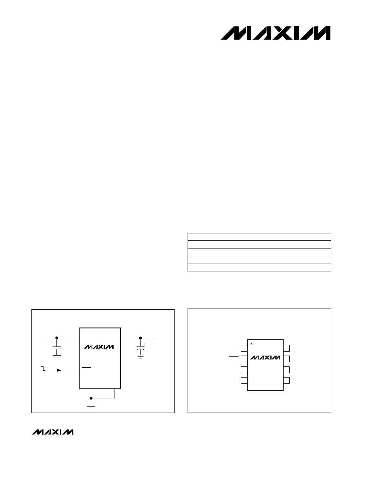
IN
OUTOUT
1
2
87GND
INSHDN
IN
SET
SO
TOP VIEW
3
4
6
5
MAX1658
MAX1659
__________________Pin Configuration
MAX1658
MAX1659
IN
SHDN
OFF
ON
INPUT
UP TO 16.5V
OUTPUT
3.3V OR 5V,
OR ADJ. (DOWN TO 1.25V);
UP TO 350mA
GND SET
OUT
__________Typical Operating Circuit
19-1263; Rev 0; 7/97
PART
MAX1658C/D
MAX1659C/D
0°C to +70°C
0°C to +70°C
TEMP. RANGE PIN-PACKAGE
Dice*
Dice*
______________Ordering Information
Dual Mode is a trademark of Maxim Integrated Products.
MAX1658ESA -40°C to +85°C 8 SO
MAX1659ESA -40°C to +85°C 8 SO
*
Dice are tested at TA= +25°C, DC parameters only.
For free samples & the latest literature: http://www.maxim-ic.com, or phone 1-800-998-8800.
For small orders, phone 408-737-7600 ext. 3468.
Page 2
MAX1658/MAX1659
350mA, 16.5V Input,
Low-Dropout Linear Regulators
2 _______________________________________________________________________________________
ABSOLUTE MAXIMUM RATINGS
ELECTRICAL CHARACTERISTICS
(VIN= 5V (MAX1658), VIN= 6V (MAX1659); C
OUT
= 10µF; SHDN = IN; TA= T
MIN
to T
MAX
; unless otherwise noted. Typical values are
at T
A
= +25°C.) (Note 2)
Stresses beyond those listed under “Absolute Maximum Ratings” may cause permanent damage to the device. These are stress ratings only, and functional
operation of the device at these or any other conditions beyond those indicated in the operational sections of the specifications is not implied. Exposure to
absolute maximum rating conditions for extended periods may affect device reliability.
IN to GND................................................................-17V to +17V
Continuous Output Current...............................................500mA
Output Short-Circuit Duration ............................................Infinite
SET, SHDN to GND.................................................-17V to +17V
OUT to GND................................................-0.3V to (VIN + 0.3V)
Continuous Power Dissipation (Note 1)
SO (derate 14.5mW/°C above +70°C) .............................1.2W
Operating Temperature Range
MAX1658ESA/MAX1659ESA............................-40°C to +85°C
Junction Temperature......................................................+150°C
Storage Temperature Range.............................-65°C to +160°C
Lead Temperature Range (soldering, 10sec)..................+300°C
SET = GND,
0mA < I
LOAD
< 350mA
V
OUT
= 5.0V
SHDN ≤ 0.4V
SET = OUT
SHDN = GND or SHDN = IN
2.7V ≤ VIN≤ 16.5V
2.7V ≤ VIN≤ 16.5V
MAX1658, VIN= 5V to 16.5V
I
OUT
= 350mA
10Hz to 100kHz
(Note 3)
I
OUT
= 0mA to 350mA
CONDITIONS
µs120t
START
Shutdown Exit Time
µA0.1 1I
QSHDN
Shutdown Supply Current
µA0.1I
SHDN
Shutdown Input Bias Current
V2.0V
INHSHDN
Logic-High Input Threshold
V0.4V
INLSHDN
Logic-Low Input
mVp-p2.5e
n
Output Noise
%V
OUT
0V
OSH
Startup Overshoot
%/mA0.003∆V
LDR
Load Regulation
V
4.85 5.00 5.15
3.20 3.30 3.40
V
OUT
V2.7 16.5V
IN
Input Voltage Range
Output Voltage
0.03
mV
490 875
∆V
DO
Dropout Voltage (Note 4) 650 1500
2
V1.25 16
Regulated Output
Voltage Range
mA350I
OUT(MAX)
Maximum Output Current
mA900I
LIM
Current Limit
µA30 60I
Q
Supply Current
UNITSMIN TYP MAXSYMBOLPARAMETER
MAX1659, VIN= 6V to 16.5V
%/V
0.05
∆V
LNR
Line Regulation
MAX1658,
5V ≤ VIN≤ 16.5V
MAX1659,
6V ≤ VIN≤ 16.5V
I
OUT
= 1mA
MAX1658
MAX1659
SHUTDOWN
Note 1: See
Operating Region and Power Dissipation
section.
Page 3
MAX1658/MAX1659
350mA, 16.5V Input,
Low-Dropout Linear Regulators
_______________________________________________________________________________________ 3
ELECTRICAL CHARACTERISTICS (continued)
(VIN= 5V (MAX1658), VIN= 6V (MAX1659); C
OUT
= 10µF; SHDN = IN; TA= T
MIN
to T
MAX
; unless otherwise noted. Typical values are
at T
A
= +25°C.) (Note 2)
Note 2: Specifications to -40°C are guaranteed by design, not production tested.
Note 3: Adjustable configuration only. V
IN
= 16.5V.
Note 4: The dropout voltage is defined as (V
IN
- V
OUT
) when V
OUT
is 100mV below the value of V
OUT
for VIN= V
OUT
+ 2V.
TA= +85°C (Note 3)
TA= +25°C (Note 3)
I
OUT
= 10µA (Note 3)
CONDITIONS
µA
0.1
I
SET
SET Input Leakage Current
0.01 0.025
V1.174 1.210 1.246V
SET
SET Reference Voltage
UNITSMIN TYP MAXSYMBOLPARAMETER
°C165T
SD
Thermal Shutdown Temperature
°C10∆T
SD
Thermal Shutdown Hysteresis
__________________________________________Typical Operating Characteristics
(VIN= 5V (MAX1658), VIN= 6V (MAX1659); SHDN = IN; SET = GND; CIN= 0.1µF; C
OUT
= 10µF tantalum; TA= +25°C; unless
otherwise noted.)
-10
-90
10 1000 10k100 100k
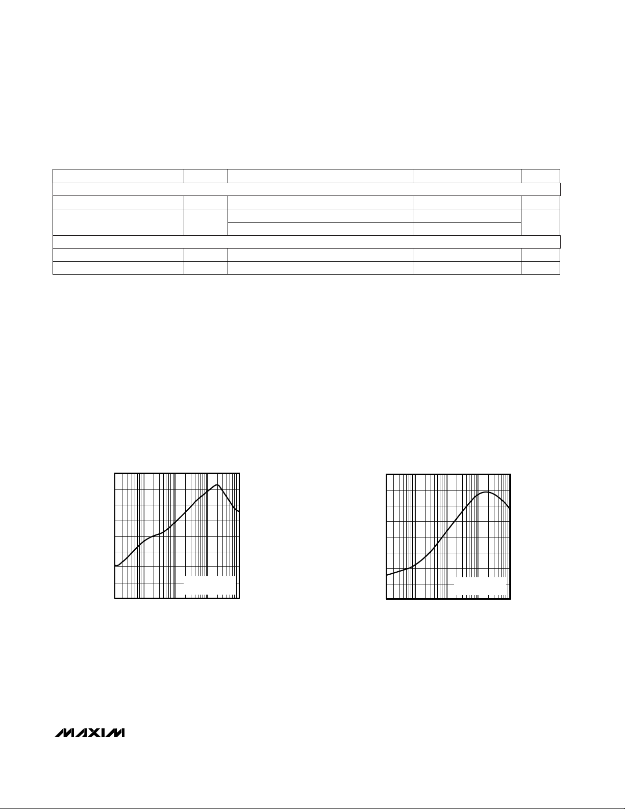
MAX1658
POWER-SUPPLY
REJECTION RATIO vs. FREQUENCY
-70
-80
MAX1658 TOC01
FREQUENCY (Hz)
PSRR (dB)
-60
-40
-50
-30
-20
VIN = 5.2V TO 5.4V
V
OUT
= 3.3V
-8
-72
10 1000 10k100 100k
MAX1659
POWER-SUPPLY
REJECTION RATIO vs. FREQUENCY
-56
-64
MAX1658 TOC03
FREQUENCY (Hz)
PSSR (dB)
-48
-32
-40
-24
-16
VIN = 6.15V TO 6.4V
V
OUT
= 5V
SET INPUT
THERMAL PROTECTION
Page 4
MAX1658/MAX1659
350mA, 16.5V Input,
Low-Dropout Linear Regulators
4 _______________________________________________________________________________________
____________________________Typical Operating Characteristics (continued)
(VIN= 5V (MAX1658), VIN= 6V (MAX1659); SHDN = IN; SET = GND; CIN= 0.1µF; C
OUT
= 10µF tantalum; TA= +25°C; unless
otherwise noted.)
0.990
0.994
0.992
0.996
0.998
1.000
0
100
200 300 400
NORMALIZED OUTPUT VOLTAGE
vs. LOAD CURRENT
MAX1658/59 TOC05
OUTPUT CURRENT (mA)
OUTPUT VOLTAGE V
NOMINAL
/V
OUT
(V)
3.3V OUTPUT
5V OUTPUT
0
20
40
60
80
0 3 6 9 1512 18
MAX1658
SUPPLY CURRENT vs. INPUT VOLTAGE
MAX1658/59 TOC06
INPUT VOLTAGE (V)
SUPPLY CURRENT (µA)
IL = 100mA
IL = 0mA
V
OUT
= 3.3V
0
500
1000
1500
2000
0 3 6 9 12 15
DROPOUT VOLTAGE
vs. OUTPUT VOLTAGE
MAX1658/59 TOC07
OUTPUT VOLTAGE (V)
DROPOUT VOLTAGE (mV)
IL = 350mA
B
A
MAX1659
LINE-TRANSIENT RESPONSE
MAX1658/59TOC10
A: INPUT VOLTAGE (1V/div), VIN = 7V (HIGH), VIN = 6V (LOW)
B: OUTPUT VOLTAGE (100mV/div)
100µs/div
V
OUT
= 5.0V
0
200
400
600
100
300
500
700
800
0 100 200 300 400
DROPOUT VOLTAGE
vs. LOAD CURRENT
MAX1658/59 TOC08
LOAD CURRENT (mA)
DROPOUT VOLTAGE (mV)
V
OUT
= 5.0V
V
OUT
= 3.3V
0
40
80
100
20
60
120
140
0 100 200 300 40050 150 250 350
QUIESCENT CURRENT
vs. LOAD CURRENT
MAX1658/59 TOC09
LOAD CURRENT (mA)
QUIESCENT CURRENT (µA)
B
A
100µs/div
MAX1658
LINE-TRANSIENT RESPONSE
MAX1658/59TOC11
A: INPUT VOLTAGE (1V/div), VIN = 6V (HIGH), VIN = 5V (LOW)
B: OUTPUT VOLTAGE (100mV/div)
V
OUT
= 3.3V
B
A
V
OUT
= 5V
MAX1659
LOAD-TRANSIENT RESPONSE
MAX1658/59TOC12
A: OUTPUT VOLTAGE (100mV/div)
B: I
OUT
= 300mA (HIGH), I
OUT
= 40mA (LOW)
200µs/div
B
A
V
OUT
= 3.3V
MAX1658
LOAD-TRANSIENT RESPONSE
MAX1658/59TOC13
A: OUTPUT VOLTAGE (100mV/div)
B: I
OUT
= 300mA (HIGH), I
OUT
= 40mA (LOW)
200µs/div
Page 5

MAX1658/MAX1659
350mA, 16.5V Input,
Low-Dropout Linear Regulators
_______________________________________________________________________________________ 5
____________________________Typical Operating Characteristics (continued)
(VIN= 5V (MAX1658), VIN= 6V (MAX1659); SHDN = IN; SET = GND; CIN= 0.1µF; C
OUT
= 10µF tantalum; TA= +25°C; unless
otherwise noted.)
B
A
0V
3.3V
100µs/div
MAX1658 OVERSHOOT AND
TIME EXITING SHUTDOWN
MAX1658/59TOC14
A: OUTPUT VOLTAGE (1V/div)
B: SHDN PIN VOLTAGE (2V/div)
B
A
0V
5V
100µs/div
MAX1659 OVERSHOOT AND
TIME EXITING SHUTDOWN
MAX1658/59TOC15
A: OUTPUT VOLTAGE (2V/div)
B: SHDN PIN VOLTAGE (2V/div)
10ms/div
10Hz TO 100kHz NOISE, V
OUT
= 5V (1mV/div), I
OUT
= 165mA
OUTPUT NOISE
______________________________________________________________Pin Description
GroundGND8
Regulated Output Voltage. Fixed or adjustable from 1.25V to 16V. Sources up to 350mA. For stable operation, bypass with a 10µF, low-ESR (<0.2Ω) capacitor from OUT to GND. For improved load-transient
response, use a larger low-ESR capacitor.
OUT4, 5
Unregulated Input Supply Voltage, 2.7V to 16.5V input range. The IN pins also serve as heatsinks. Connect
to a copper plane to achieve maximum thermal dissipation.
IN3, 6, 7
PIN
Shutdown Input. When SHDN is low, the device turns off and typically draws 0.1µA of supply current.SHDN
2
Output Voltage Input. Connecting SET to ground selects the factory-preset 3.3V (MAX1658) or 5V
(MAX1659) output voltage. For an adjustable output voltage, connect SET to a resistive voltage divider from
OUT to GND.
SET1
FUNCTIONNAME
/√Hz)
RMS
OUTPUT NOISE DENSITY
vs. FREQUENCY
4
10
3
10
MAX1658 TOC02
2
10
OUTPUT NOISE DENSITY (nV
10
10 50k
FREQUENCY (Hz)
V
I
OUT
OUT
= 5V
= 165mA
Page 6

MAX1658/MAX1659
350mA, 16.5V Input,
Low-Dropout Linear Regulators
6 _______________________________________________________________________________________
MAX1658
MAX1659
P
P
OUT
SET
IN
SHDN
MOSFET
DRIVER
WITH
CURRENT
LIMIT
R2
R1
65mV
GND
DUAL-MODE
COMPARATOR
1.21V
REFERENCE
THERMAL
SENSOR
ERROR
AMPLIFIER
Figure 1. Functional Diagram
_______________Detailed Description
The MAX1658/MAX1659 are micropower, low-dropout
linear regulators featuring Dual Mode™ operation,
which allows them to deliver an adjustable (1.25V to
16.5V) or preset (3.3V for the MAX1658, 5V for
MAX1659) output. They supply up to 350mA while
requiring only 120µA of supply current (typically 30µA
with no load). The devices include thermal shutdown
circuitry, output current limiting, a P-channel pass transistor, a Dual Mode comparator, and a feedback voltage divider. Figure 1 shows the functional diagram.
The 1.21V reference is connected to the amplifier’s
inverting input. The error amplifier compares this reference with the selected feedback voltage and amplifies
the difference. The error signal applies the drive to the
P-channel pass transistor. If the feedback voltage is
lower than the reference voltage, the transistor’s gate is
pulled lower, increasing output current.
The output voltage is fed back through an internal
resistor network or an external user-selected network.
The Dual Mode comparator examines the voltage at the
SET pin and selects either the internal or external feedback path. If SET is below 65mV, internal feedback sets
the MAX1658’s output voltage to 3.3V and the
MAX1659’s to 5V. Otherwise, external feedback is used
for an adjustable output between 1.25V and 16.5V.
Additional features include internal current limiting,
reverse battery protection, thermal-overload protection,
and a 1µA shutdown mode.
Page 7

MAX1658/MAX1659
350mA, 16.5V Input,
Low-Dropout Linear Regulators
_______________________________________________________________________________________ 7
P-Channel Pass Transistor
The MAX1658/MAX1659 feature an internal P-channel
MOSFET pass transistor. Using a MOSFET provides
several advantages over similar PNP designs, including
lower dropout voltage and extended battery life. Unlike
bipolar transistors, MOSFETs reduce quiescent current,
because they require no base current, particularly at
heavy loads and in dropout. As a result, the
MAX1658/MAX1659 operate at a low quiescent current
even in dropout.
Output Voltage Selection
Dual Mode operation allows the MAX1658/MAX1659 to
operate at either a preset or a user-adjustable output
voltage. The device compares the SET pin voltage with
an internal 65mV reference. If the voltage is lower than
65mV (typically achieved by grounding SET), the
device switches to an internal resistor-divider feedback
network that sets the output voltage. The MAX1658’s
preset output voltage is 3.3V and the MAX1659’s is 5V
(Figure 2).
If the SET pin is not below 65mV, the device switches to
external feedback and SET becomes a feedback input.
The feedback network can be configured to produce
an output between 16V and the voltage reference
(nominally 1.21V). Under regulation, the feedback
mechanism adjusts the error signal such that the voltage at the SET pin equals the reference voltage.
Therefore, to achieve the minimum output, connect SET
directly to OUT. For other voltages, a resistive voltagedivider network is necessary. Figure 3 shows the topol-
ogy of a typical circuit operating in adjustable mode.
The output voltage is set by the following equation:
where V
SET
= 1.21V. Solving for R1 yields:
The input leakage current of the SET input is less than
25nA. This allows the use of large resistors in the feedback network to minimize output current loss without
compromising accuracy. R2 can be as high as 500kΩ
in most applications.
Shutdown
A logic low on the SHDN pin places the MAX1658/
MAX1659 in shutdown. This mode deactivates all functions, including the pass transistor. The device consumes less than 1µA of supply current in shutdown,
and its output becomes high impedance. The
MAX1658/MAX1659 exit shutdown in 100µs.
Output Current Limit
The MAX1658/MAX1659 include current-limiting circuitry that monitors and controls the pass transistor and
limits output current to around 900mA. The output can
be shorted to ground indefinitely without damaging the
device.
R1 = R2
V
V
1
OUT
SET
−
V V
R
R
OUT SET
= +
1
1
2
MAX1658
(MAX1659)
SHDN
2
4, 5
8 1
3, 6, 7
IN
INPUT
VOLTAGE
ON
OFF
OUTPUT VOLTAGE
3.3V/350mA
(5V/350mA)
10µF
0.1µF
GND SET
OUT
Figure 2. Preset Output Configuration
MAX1658
MAX1659
IN
3, 6, 7
4, 5
1
8
2
SHDN
OUTPUT
VOLTAGE
C
OUT
10µF
R1
R2
0.1µF
INPUT
VOLTAGE
GND
OUT
SET
V
OUT
= V
SET
(1 + R1
)
R2
V
SET
= 1.21V
Figure 3. Adjustable Output Configuration Using External
Feedback Resistors
Page 8

Thermal-Overload Protection
Thermal-overload protection limits total power dissipation in the MAX1658/MAX1659. When the junction temperature exceeds TJ= +165°C, the pass transistor
deactivates, allowing the IC to cool. Once it has cooled
by 10°C, the control logic will enable operation. Under
thermal overload, the output of the device will pulse as
the die heats up and then cools to operational levels.
Prolonged operation under these conditions is not recommended.
Operating Region and Power Dissipation
Maximum power dissipation of the MAX1658/MAX1659
depends on the thermal resistance of the package and
circuit board, the temperature difference between the
die and ambient air, and the rate of air flow. The power
dissipation by the device is P = I
OUT(VIN
- V
OUT
). The
maximum power dissipation is:
where (TJ- TA) is the temperature difference between
MAX1658/MAX1659 die junction and the surrounding
air, θJBis the thermal resistance of the package, and
θBAis the thermal resistance through the printed circuit
board, copper traces, and other materials to the
surrounding air. The 8-pin SO package for the
MAX1658/MAX1659 features a special lead frame with
a lower thermal resistance and higher allowable power
dissipation than a standard SO-8. The thermal resistance of this package is θJB= 69°C/W, compared with
θJB= 170°C/W for an SO-8.
The IN pins of the MAX1658/MAX1659 package perform the dual function of providing an electrical connection to IN and channeling heat away. Connect all IN
pins to the input voltage using a large pad or power
plane on the surface. Where this is impossible, connect
to a copper plane on an adjacent layer. The pad should
meet the dimensions specified in Figure 4.
Figure 4 assumes the IC is soldered directly to the pad,
has a +125°C maximum junction temperature and a
+25°C ambient air temperature, and has no other heat
sources. Use larger pad sizes for lower junction temperatures, higher ambient temperatures, or conditions
where the IC is not soldered directly to a heat-sinking
IN pad.
The MAX1658/MAX1659 can regulate currents up to
350mA and operate with input voltages up to 16.5V, but
not simultaneously. High output currents can only be
sustained when input-output differential voltage is low,
as shown in the following equation. Maximum power
dissipation depends on packaging, board layout, temperature, and air flow. The maximum output current is:
where P
MAX
is derived from the TJ= 125°C curve of
Figure 4.
Reverse Battery Protection
The MAX1658/MAX1659 feature reverse battery protection. Under normal operation, a P-channel MOSFET
connects the substrate of the device to IN. When the
input voltage falls below ground (implying reverse battery conditions), the P-channel switch turns off and disconnects the substrate from IN, disabling the device.
The maximum reverse battery voltage allowed is -17V.
SHDN also withstands reverse battery conditions and
can be connected directly to IN with no loss of protection.
Polarized input bypass capacitors will be damaged
under reverse battery conditions. To ensure circuit reliability, use a non-polarized capacitor at the input.
The MAX1658/MAX1659 do not provide reverse current
protection. If V
OUT
is greater than VINby more than
300mV, reverse current will flow. Reverse current protection can be added by connecting a Schottky diode
in series with IN.
I
P x C T
V V x C
OUT MAX
MAX A
IN OUT
( )
=
° −
( )
−
( )
°
125
100
P
T T
MAX
J A
JB BA
=
−
( )
+
( )
θ θ
MAX1658/MAX1659
350mA, 16.5V Input,
Low-Dropout Linear Regulators
8 _______________________________________________________________________________________
1600
1400
1200
1000
800
600
400
0.1
0.65
1
6.5
COPPER GROUND PAD AREA
10 (in
2
)
65 (cm
2
)
POWER DISSIPATION (mW)
Tj = +125°C
T
j
= +85°C
SINGLE-SIDED 1oz. COPPER
T
A
= +25°C, STILL AIR
Figure 4. Typical Maximum Power Dissipation vs. Ground Pad
Area
Page 9

__________Applications Information
Output Capacitor Selection and Stability
To maintain stability, connect a ≥10µF capacitor with
less than 200mΩ equivalent series resistance (ESR)
from OUT to GND. Larger output capacitors improve
load-transient response. Currents lower than 350mA
make the use of smaller output capacitors possible.
Table 1 shows the maximum output current typically
achieved using various output capacitors. Output voltages higher than 3.3V require less output capacitance
to remain stable.
Table 1. Typical Load Current Capabilities
Input Bypass Capacitor
The use of a 0.1µF to 10µF input bypass capacitor is
recommended. Larger capacitors provide better supply-noise rejection and line-transient response, as well
as improved performance when the supply has a high
AC impedance. Polarized input bypass capacitors will
be damaged under reverse battery conditions. If
reverse input voltages are expected, use a non-polarized capacitor at the input.
Noise and PSRR
The MAX1658/MAX1659 exhibit 2.5mVp-p of noise during normal operation. This noise level is negligible in
most applications.
The MAX1658/MAX1659 are designed to maintain
excellent power-supply rejection (55dB) at 50Hz/60Hz
(or 50dB at 120Hz). These regulators are ideal for wallcube applications that may contain significant ripple.
Larger input and output capacitors will further improve
the circuit’s AC response. See the Power-Supply
Rejection Ratio vs. Frequency graphs in the
Typical
Operating Characteristics.
MAX1658/MAX1659
350mA, 16.5V Input,
Low-Dropout Linear Regulators
_______________________________________________________________________________________ 9
OUTPUT CAPACITOR
0mA to 120mA2.2µF tantalum
LOAD CURRENT RANGE
0mA to 250mA4.7µF tantalum
0mA to 350mA10µF tantalum
___________________Chip Information
TRANSISTOR COUNT: 207
Page 10

MAX1658/MAX1659
350mA, 16.5V Input,
Low-Dropout Linear Regulators
10 ______________________________________________________________________________________
________________________________________________________Package Information
SOICN.EPS
Page 11

MAX1658/MAX1659
350mA, 16.5V Input,
Low-Dropout Linear Regulators
______________________________________________________________________________________ 11
NOTES
Page 12

MAX1658/MAX1659
350mA, 16.5V Input,
Low-Dropout Linear Regulators
NOTES
Maxim cannot assume responsibility for use of any circuitry other than circuitry entirely embodied in a Maxim product. No circuit patent licenses are
implied. Maxim reserves the right to change the circuitry and specifications without notice at any time.
12
____________________Maxim Integrated Products, 120 San Gabriel Drive, Sunnyvale, CA 94086 408-737-7600
© 1997 Maxim Integrated Products Printed USA is a registered trademark of Maxim Integrated Products.
 Loading...