

Page 1
For free samples & the latest literature: http://www.maxim-ic.com, or phone 1-800-998-8800.
For small orders, phone 1-800-835-8769.
General Description
The MAX1645 is a high-efficiency battery charger
capable of charging batteries of any chemistry type. It
uses the Intel System Management Bus (SMBus) to
control voltage and current charge outputs.
When charging lithium-ion (Li+) batteries, the MAX1645
automatically transitions from regulating current to regulating voltage. The MAX1645 can also limit line input
current so as not to exceed a predetermined current
drawn from the DC source. A 175sec charge safety
timer prevents “runaway charging” should the
MAX1645 stop receiving charging voltage/current commands.
The MAX1645 employs a next-generation synchronous
buck control circuitry that lowers the minimum input-tooutput voltage drop by allowing the duty cycle to
exceed 99%. The MAX1645 can easily charge one to
four series Li+ cells.
Applications
Notebook Computers
Point-of-Sale Terminals
Personal Digital Assistants
Features
♦ Input Current Limiting
♦ 175sec Charge Safety Timeout
♦ 128mA Wake-Up Charge
♦ Charges Any Chemistry Battery:
Li+, NiCd, NiMH, Lead Acid, etc.
♦ Intel SMBus 2-Wire Serial Interface
♦ Compliant with Level 2 Smart Battery Charger
Spec. Rev. 1.0
♦ +8V to +28V Input Voltage Range
♦ Up to 18.4V Battery Voltage
♦ 11-Bit Battery Voltage Setting
♦ ±0.8% Output Voltage Accuracy with Internal
Reference
♦ 3A max Battery Charge Current
♦ 6-Bit Charge Current Setting
♦ 99.99% max Duty Cycle for Low-Dropout Operation
♦ Load/Source Switchover Drivers
♦ >97% Efficiency
MAX1645
Advanced Chemistry-Independent, Level 2
Battery Charger with Input Current Limiting
________________________________________________________________
Maxim Integrated Products
1
19-1566; Rev 0a; 10/99
PART
MAX1645EEI -40°C to +85°C
TEMP. RANGE PIN-PACKAGE
28 QSOP
Typical Operating Circuit appears at end of data sheet.
SMBus is a trademark of Intel Corp.
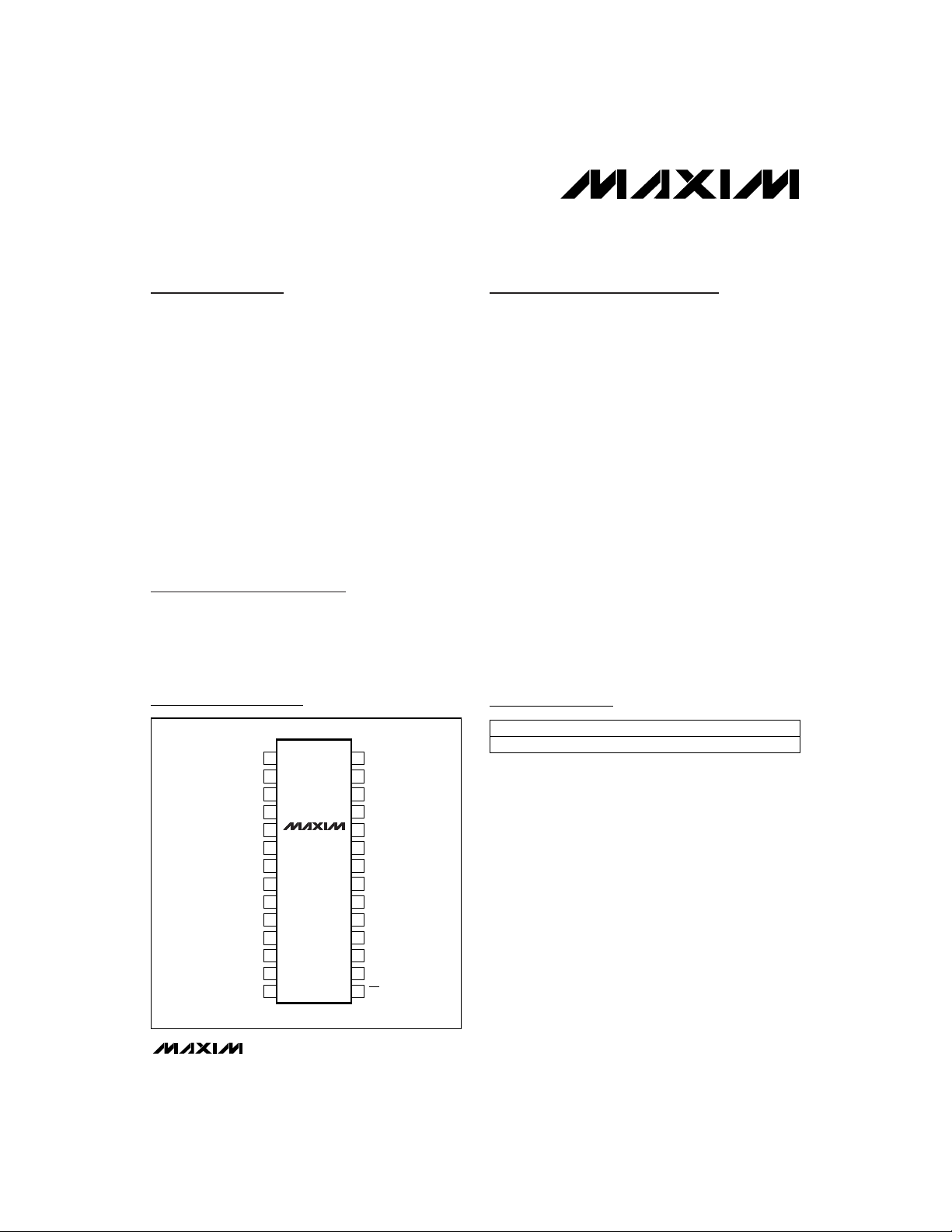
Pin Configuration
Ordering Information
TOP VIEW
1
DCIN
2
LDO
3
CLS
4
REF
5
CCS
6
CCI
7
CCV
8
GND
9
BATT
10
DAC
11
V
DD
12
THM
13
SCL
14
SDA
MAX1645
QSOP
28
27
26
25
24
23
22
21
20
19
18
17
16
15
CVS
PDS
CSSP
CSSN
BST
DHI
LX
DLOV
DLO
PGND
CSIP
CSIN
PDL
INT
Page 2
MAX1645
Advanced Chemistry-Independent, Level 2
Battery Charger with Input Current Limiting
2 _______________________________________________________________________________________
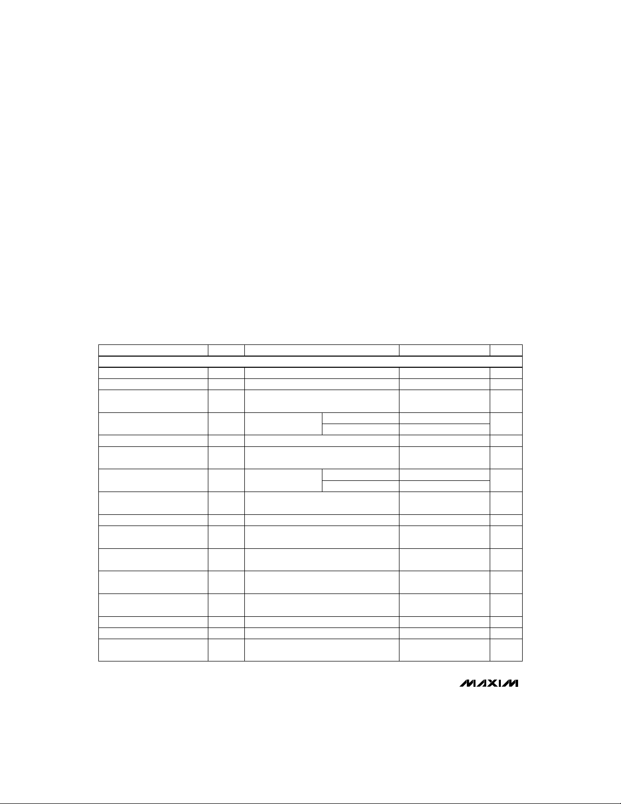
ABSOLUTE MAXIMUM RATINGS
ELECTRICAL CHARACTERISTICS
(Circuit of Figure 1, VDD= +3.3V, V
BATT
= +16.8V, V
DCIN
= +18V, TA= 0°C to +85°C, unless otherwise noted. Typical values are at
T
A
= +25°C.)
Stresses beyond those listed under “Absolute Maximum Ratings” may cause permanent damage to the device. These are stress ratings only, and functional
operation of the device at these or any other conditions beyond those indicated in the operational sections of the specifications is not implied. Exposure to
absolute maximum rating conditions for extended periods may affect device reliability.
DCIN, CVS, CSSP, CSSN, LX to GND....................-0.3V to +30V
CSSP to CSSN, CSIP to CSIN ...............................-0.3V to +0.3V
PDS, PDL to GND ...................................-0.3V to (V
CSSP
+ 0.3V)
BST to LX..................................................................-0.3V to +6V
DHI to LX...................................................-0.3V to (V
BST
+ 0.3V)
CSIP, CSIN, BATT to GND .....................................-0.3V to +22V
LDO to GND.....................-0.3V to (lower of 6V or V
DCIN
+ 0.3V)
DLO to GND ...........................................-0.3V to (V
DLOV
+ 0.3V)
REF, DAC, CCV, CCI, CCS, CLS to GND.....-0.3V to (V
LDO
+ 0.3V)
V
DD
, SCL, SDA, INT, DLOV to GND.........................-0.3V to +6V
THM to GND...............................................-0.3V to (V
DD
+ 0.3V)
PGND to GND .......................................................-0.3V to +0.3V
LDO Continuous Current.....................................................50mA
Continuous Power Dissipation (T
A
= +70°C)
28-Pin QSOP (derate 10.8mW/°C above +70°C).......860mW
Operating Temperature Range ...........................-40°C to +85°C
Storage Temperature.........................................-60°C to +150°C
Lead Temperature (soldering, 10sec).............................+300°C
8V < V
DCIN
< 28V
V
CVS
referred to V
BATT
, V
CVS
rising
V
PDS
= V
CSSP
- 2V, V
DCIN
= 16V
PDS = CSSP
I
PDS
= 0
0 < V
DCIN
< 6V, VDD= 5V, V
SCL
= 5V,
V
SDA
= 5V
V
CVS
referred to V
BATT
V
CVS
referred to V
BATT
, V
CVS
falling
When the SMB responds to commands
8V < V
DCIN
< 28V
8V < V
DCIN
< 28V
When AC_PRESENT
switches
When I
CHARGE
drops to 128mA
8V < V
DCIN
< 28V, 0 < I
LDO
< 15mA
0 < I
REF
< 200µA
CONDITIONS
mV
-150 -100 -50
V
PDL-OFF
PDL Load Switch Turn-Off
Threshold
mA
10 50
PDS Turn-Off Current
µA
100 150 300
PDS Turn-On Current
V
81012
PDS Output Low Voltage, PDS
Below CSSP
mV
100 200 300
V
PDS-HYS
PDS Charging Source Switch
Threshold Hysteresis
mV
50 100 150
V
PDS-OFF
PDS Charging Source Switch
Turn-Off Threshold
V
2.4 2.8
BATT Undervoltage Threshold
(Note 2)
V
4.066 4.096 4.126
V
REF
REF Output Voltage
mA
1.7 6
I
DCIN
DCIN Supply Current
V
828
V
DCIN
µA
80 150
I
DD
VDDQuiescent Current
2.1 2.5
V
2.55 2.8
VDDUndervoltage Threshold
V
2.8 5.65
VDDInput Voltage Range
(Note 1)
mA
0.7 2
DCIN Supply Current Charging
Inhibited
V
7.5 7.85
DCIN Undervoltage Threshold
7 7.4
V
5.15 5.4 5.65
V
LDO
LDO Output Voltage
UNITSMIN TYP MAXSYMBOLPARAMETER
DCIN rising
DCIN falling
VDDrising
VDDfalling
DCIN Typical Operating Range
GENERAL SPECIFICATIONS
Page 3
MAX1645
Advanced Chemistry-Independent, Level 2
Battery Charger with Input Current Limiting
_______________________________________________________________________________________ 3
ELECTRICAL CHARACTERISTICS (continued)
(Circuit of Figure 1, VDD= +3.3V, V
BATT
= +16.8V, V
DCIN
= +18V, TA= 0°C to +85°C, unless otherwise noted. Typical values are at
T
A
= +25°C.)
V
CCV
= V
CCI
= V
CCS
= 0.25V to 2V
PDL to GND
From CSSP/CSSN to CCS, V
CLS
= 2.048V,
V
CSSP
- V
CSSN
= 102.4mV
From BATT to CCV
V
CSSN
- V
PDL
= 1V
V
CSSP
= V
CSSN
= 28V, V
DCIN
= 0
V
CVS
referred to V
BATT
V
CSSP
= V
CSSN
= V
DCIN
= 0 to 28V
Total of I
BATT
, I
CSIP,
and I
CSIN
;
V
BATT
= 0 to 20V, V
DCIN
= 0
Total of I
BATT
, I
CSIP,
and I
CSIN
;
V
BATT
= 0 to 20V, charge inhibited
R
CSS
= 40mΩ
Total of I
BATT
, I
CSIP,
and I
CSIN
;
V
BATT
= 0 to 20V
R
CS
= 50mΩ
Charging Voltage() = 0x1060
V
CVS
= 28V
ChargingVoltage() = 0x41A0
ChargingVoltage() = 0x3130
V
BATT
= 1V, R
CSI
= 50mΩ
ChargingVoltage() = 0x20D0
CONDITIONS
From CSIP/SCIN to CCI, ChargingCurrent() =
0x0BC0, V
CSIP
- V
CSIN
= 150.4mV
From BATT to CCV, ChargingVoltage() =
0x41A0, V
BATT
= 16.8V
V
CLS
= V
REF
/2 to V
REF
mV
150 300 600
CCV/CCI/CCS Clamp Voltage
(Note 4)
µA/mV
V/V
200 500
Battery Voltage-Error Amp DC
Gain
µA
-1 1
CSSP/CSSN Quiescent Current
µA-100 540 1000CSSP Input Bias Current
µA
-5 5
Total BATT Standby Current
µA
-100 100
Total BATT Quiescent Current
µA
-700 700
Total BATT Input Bias Current
V
020
BATT/CSIP/CSIN Input Voltage
Range
mA
20 128 200
BATT Undervoltage Charge
Current
2.282 2.56 2.838
kΩ
50 100 150
PDL Turn-On Resistance
mA
612
mV
100 200 300
V
PDL-HYS
PDL Load Switch Threshold
Hysteresis
PDL Turn-Off Current
A
4.714 5.12 5.526
mA
61.6 128 194.4
A
2.798 3.008 3.218
I0BATT Charge Current (Note 3)
4.150 4.192 4.234
µA
620
CVS Input Bias Current
16.666 16.8 16.934
V0BATT Full-Charge Voltage V
12.492 12.592 12.692
8.333 8.4 8.467
UNITSMIN TYP MAXSYMBOLPARAMETER
0.5 1 2
Input Current-Error Amp
Transconductance
µA/mV
0.5 1 2
Battery Current-Error Amp
Transconductance
µA/mV
0.111 0.222 0.444
Battery Voltage-Error Amp
Transconductance
µA
-1 0.05 1
CLS Input Bias Current
DCIN Source Current Limit
(Note 3)
ChargingCurrent() =
0x0BC0
ChargingCurrent() =
0x0080
V
CLS
= 4.096V
V
CLS
= 2.048V
V
CSSP
= C
CSSN
= V
DCIN
= 0 to 28V mA-100 35 100CSSN Input Bias Current
Page 4
MAX1645
Advanced Chemistry-Independent, Level 2
Battery Charger with Input Current Limiting
4 _______________________________________________________________________________________
V
SDA
= 0.4V
All 4 comparators, VDD= 2.8V to 5.65V
VDD= 2.8V to 5.65V, V
THM
falling
VDD= 2.8V to 5.65V, V
THM
falling
DLO high or low, V
DLOV
= 4.5V
DHI high or low, V
BST
- VLX= 4.5V
VDD= 2.8V to 5.65V, V
THM
falling
VDD= 2.8V to 5.65V, V
THM
falling
R
CSI
= 50mΩ
V
DLOV
= V
LDO
, DLO low
V
DCIN
= 28V, V
BATT
= VLX= 20V
V
DCIN
= 0, V
BATT
= VLX= 20V
V
THM
= 4% of VDDto 96% of VDD,
V
DD
= 2.8V to 5.65V
DHI high
CONDITIONS
mA
6
SDA Output Low Sink Current
µA
-1 1
SDA/SCL Input Bias Current
mV
220
SDA/SCL Input Hysteresis
V
1.4
SDA/SCL Input High Voltage
V
0.6
SDA/SCL Input Low Voltage
1
Thermistor Comparator
Threshold Hysteresis
6 7.5 9
Thermistor Underrange
Threshold
% of V
DD
22 23.5 25
Thermistor Hot Threshold
74 75.5 77
Thermistor Cold Threshold
89.5 91 92.5
Thermistor Overrange Threshold
µA-1 1THM Input Bias Current
ms
51015
t
ON
Maximum On-Time
µs
1 1.25 1.5
t
OFF
Minimum Off-Time
Ω
614
DLO Output Resistance
Ω
6 14
DHI Output Resistance
A
5.0 6.0 7.0
Inductor Peak Current Limit
µA
5 10
DLOV Supply Current
%
99 99.99
Maximum Duty Cycle
µA
200 500
LX Input Bias Current
µA
1
LX Input Quiescent Current
µA
615
BST Supply Current
UNITSMIN TYP MAXSYMBOLPARAMETER
I
INT
= 1mA
V
INT
= 5.65V
mV
25 200
µA
1
INT Output High Leakage
INT Output Low Voltage
ns
0
t
HD:DAT
SDA Hold Time from SCL
ns
250
t
SU:DAT
SDA Setup Time from SCL
µs
4
t
HIGH
SCL High Period
µs
4.7
t
LOW
SCL Low Period
µs
4.7
t
SU:STA
Start Condition Setup Time
from SCL
µs
4
t
HD:STA
Start Condition Hold Time
from SCL
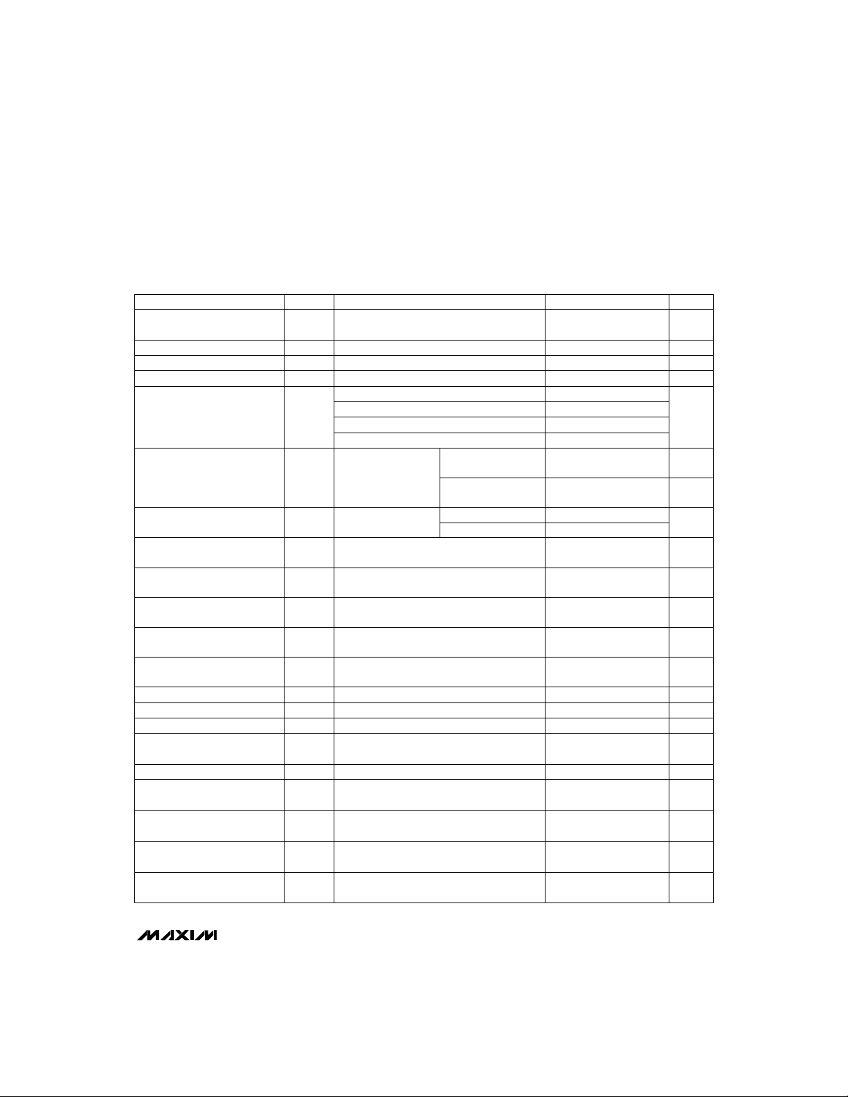
ELECTRICAL CHARACTERISTICS (continued)
(Circuit of Figure 1, VDD= +3.3V, V
BATT
= +16.8V, V
DCIN
= +18V, TA= 0°C to +85°C, unless otherwise noted. Typical values are at
T
A
= +25°C.)
% of V
DD
% of V
DD
% of V
DD
% of V
DD
DC-TO-DC CONVERTER SPECIFICATIONS
THERMISTOR COMPARATOR SPECIFICATIONS
SMB INTERFACE LEVEL SPECIFICATIONS (VDD= 2.8V to 5.65V)
SMB INTERFACE TIMING SPECIFICATIONS (VDD= 2.8V to 5.65V, Figures 4 and 5)
Page 5
MAX1645
Advanced Chemistry-Independent, Level 2
Battery Charger with Input Current Limiting
_______________________________________________________________________________________ 5
ELECTRICAL CHARACTERISTICS (continued)
(Circuit of Figure 1, VDD= +3.3V, V
BATT
= +16.8V, V
DCIN
= +18V, TA= 0°C to +85°C, unless otherwise noted. Typical values are at
T
A
= +25°C.)
CONDITIONS UNITSMIN TYP MAXSYMBOLPARAMETER
sec
140 175 210
t
WDT
Maximum Charge Period
Without a ChargingVoltage() or
Charging Current() Loaded
µs
1
t
DV
SDA Output Data Valid from SCL
ELECTRICAL CHARACTERISTICS
(Circuit of Figure 1, VDD= +3.3V, V
BATT
= +16.8V, V
DCIN
= +18V, TA= -40°C to +85°C, unless otherwise noted. Guaranteed by design.)
PARAMETER SYMBOL MIN MAX UNITS
LDO Output Voltage V
LDO
5.15 5.65
V
7
DCIN Undervoltage Threshold
7.85
V
DCIN Supply Current Charging
Inhibited
2
mA
VDDInput Voltage Range
(Note 1)
2.8 5.65
V
VDDUndervoltage Threshold
2.8
V
2.1
VDDQuiescent Current I
DD
150
µA
DCIN Typical Operating Range V
DCIN
828
V
DCIN Supply Current I
DCIN
6
mA
REF Output Voltage V
REF
4.035 4.157
V
BATT Undervoltage Threshold
(Note 2)
2.4 2.8
V
PDS Charging Source Switch
Turn-Off Threshold
V
PDS-OFF
50 150
mV
PDS Charging Source Switch
Threshold Hysteresis
V
PDS-HYS
100 300
mV
PDS Output Low Voltage, PDS
Below CSSP
812
V
PDS Turn-On Current
100 300
µA
PDS Turn-Off Current
10
mA
PDL Load Switch Turn-Off
Threshold
V
PDL-OFF
-150 -50
mV
PDL Load Switch Threshold
Hysteresis
V
PDL-HYS
100 300
mV
PDL Turn-Off Current
6
mA
CONDITIONS
0 < I
REF
< 200µA
8V < V
DCIN
< 28V, 0 < I
LDO
< 15mA
When I
CHARGE
drops to 128mA
When AC_PRESENT
switches
8V < V
DCIN
< 28V
8V < V
DCIN
< 28V
When the SMB responds to commands
V
CVS
referred to V
BATT
, V
CVS
falling
V
CVS
referred to V
BATT
0 < V
DCIN
< 6V, VDD= 5V, V
SCL
= 5V,
V
SDA
= 5V
I
PDS
= 0
PDS = CSSP
V
PDS
= V
CSSP
- 2V, V
DCIN
= 16V
V
CVS
referred to V
BATT
, V
CVS
rising
V
CVS
referred to V
BATT
V
CSSN
- V
PDL
= 1V
8V < V
DCIN
< 28V
DCIN rising
DCIN falling
VDDrising
VDDfalling
GENERAL SPECIFICATIONS
Page 6
MAX1645
Advanced Chemistry-Independent, Level 2
Battery Charger with Input Current Limiting
6 _______________________________________________________________________________________
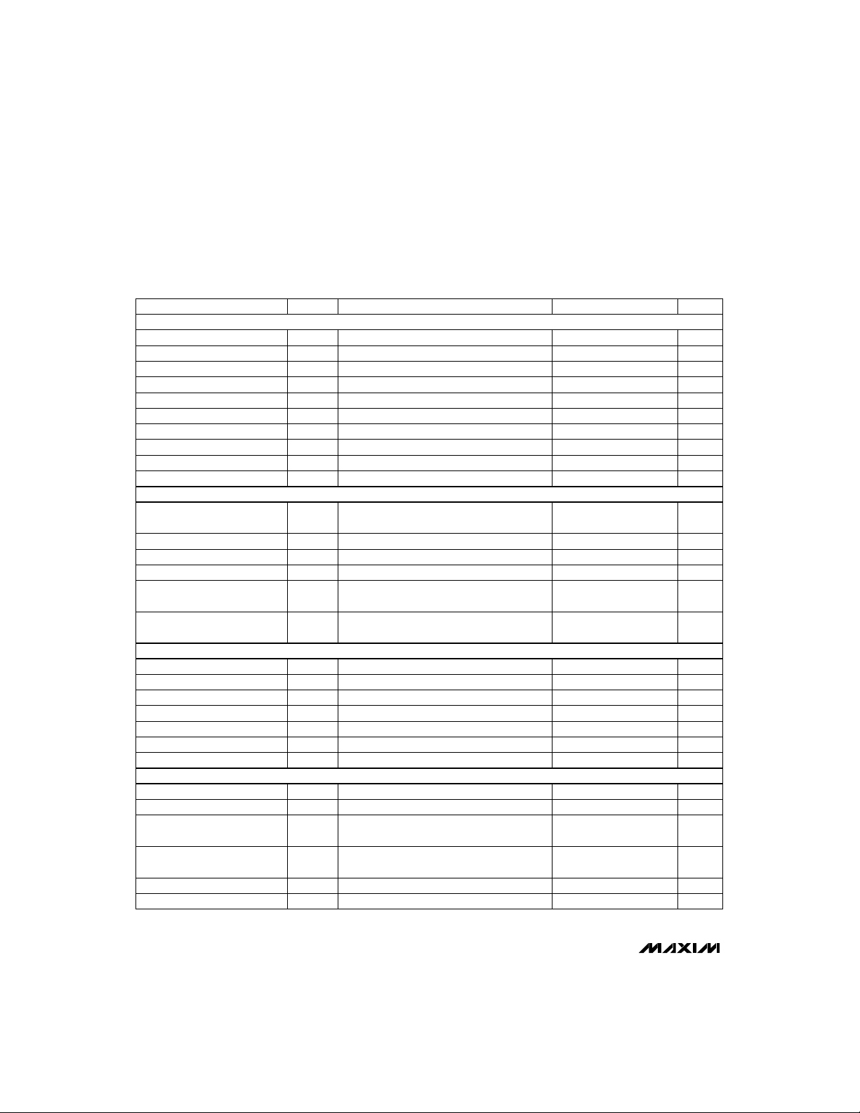
ELECTRICAL CHARACTERISTICS (continued)
(Circuit of Figure 1, VDD= +3.3V, V
BATT
= +16.8V, V
DCIN
= +18V, TA= -40°C to +85°C, unless otherwise noted. Guaranteed by design.)
Maximum Duty Cycle
99
%
Minimum Off-Time t
OFF
1 1.5
µs
Maximum On-Time t
ON
515
ms
PARAMETER SYMBOL MIN MAX UNITS
4.124 4.260
8.266 8.534
12.391 12.793
BATT Full-Charge Voltage V0
16.532 17.068
V
BATT Charge Current (Note 3) I0
2.608 3.408
A
15.2 240.8
mA
DCIN Source Current Limit
(Note 3)
4.358 5.882
A
2.054 3.006
CVS Input Bias Current
PDL Turn-On Resistance
50 150
kΩ
20
µA
BATT Undervoltage Charge
Current
20 200
mA
BATT/CSIP/CSIN Input Voltage
Range
020
V
Total BATT Input Bias Current
-700 700
µA
Total BATT Quiescent Current
-100 100
µA
Total BATT Standby Current
-5 5
µA
CSSP/Input Bias Current
-100 1000
µA
CSSP/CSSN Quiescent Current
-1 1
µA
Battery Voltage-Error Amp DC
Gain
200
V/V
CLS Input Bias Current
-1 1
µA
Battery Voltage-Error Amp
Transconductance
0.111 0.444
µA/mV
Battery Current-Error Amp
Transconductance
0.5 2
µA/mV
Input Current-Error Amp
Transconductance
0.5 2
µA/mV
CCV/CCI/CCS Clamp Voltage
(Note 4)
150 600
mV
CONDITIONS
V
BATT
= 1V, R
CSI
= 50mΩ
ChargingVoltage() = 0x1060
ChargingVoltage() = 0x20D0
ChargingVoltage() = 0x3130
ChargingVoltage() = 0x41A0
R
CSI
= 50mΩ
Total of I
BATT
, I
CSIP,
and I
CSIN
;
V
BATT
= 0 to 20V
Total of I
BATT
, I
CSIP,
and I
CSIN
;
V
BATT
= 0 to 20V, charge inhibited
R
CSS
= 40mΩ
Total of I
BATT
, I
CSIP,
and I
CSIN
;
V
BATT
= 0 to 20V, V
DCIN
= 0
V
CSSP
= V
CSSN
= V
DCIN
= 28V
V
CSSP
= V
CSSN
= 28V, V
DCIN
= 0
PDL to GND
From BATT to CCV
V
CVS
= 28V
V
CLS
= V
REF
/2 to V
REF
From BATT to CCV, ChargingVoltage() =
0x41A0, V
BATT
= 16.8V
From CSIP/CSIN to CCI, ChargingCurrent() =
0x0BC0, V
CSIP-VCSIN
= 150.4mV
From CSSP/CSSN to CCS, V
CLS
= 2.048V,
V
CSSP
- V
CSSN
= 102.4mV
V
CCV
= V
CCI
= V
CCS
= 0.25V to 2V
ChargingCurrent() =
0x0BC0
ChargingCurrent() =
0x0080
V
CLS
= 4.096V
V
CLS
= 2.048V
CSSN Input Bias Current
-100 100
µAV
CSSP
= V
CSSN
= V
DCIN
= 28V
DC-TO-DC CONVERTER SPECIFICATIONS
ERROR AMPLIFIER SPECIFICATIONS
Page 7
MAX1645
Advanced Chemistry-Independent, Level 2
Battery Charger with Input Current Limiting
_______________________________________________________________________________________ 7
ELECTRICAL CHARACTERISTICS (continued)
(Circuit of Figure 1, VDD= +3.3V, V
BATT
= +16.8V, V
DCIN
= +18V, TA= -40°C to +85°C, unless otherwise noted. Guaranteed by design.)
SDA Hold Time from SCL t
HD:DAT
0
ns
Start Condition Hold Time
from SCL
Start Condition Setup Time
from SCL
t
SU:STA
4.7
µs
t
HD:STA
4
µs
SDA Setup Time from SCL t
SU:DAT
250
ns
PARAMETER SYMBOL MIN MAX UNITS
DLO Output Resistance
14
Ω
DHI Output Resistance
14
Ω
Inductor Peak Current Limit
5.0 7.0
A
DLOV Supply Current
10
µA
THM Input Bias Current
-1 1
µA
Thermistor Overrange Threshold
89.5 92.5
Thermistor Cold Threshold
74 77
LX Input Quiescent Current
LX Input Bias Current
500
µA
1
µA
BST Supply Current
15
µA
Thermistor Hot Threshold
22 25
% of V
DD
Thermistor Underrange
Threshold
69
SDA/SCL Input Low Voltage
0.6
V
SDA/SCL Input High Voltage
1.4
V
SDA/SCL Input Bias Current
-1 1
µA
SDA Output Low Sink Current
6
mA
INT Output High Leakage
1
µA
INT Output Low Voltage
200
mV
SCL High Period t
HIGH
4
µs
SCL Low Period t
LOW
4.7
µs
CONDITIONS
VDD= 2.8V to 5.65V, V
THM
falling
DLO high or low, V
DLOV
= 4.5V
VDD= 2.8V to 5.65V, V
THM
falling
DHI high or low, V
BST
- VLX= 4.5V
R
CSI
= 50mΩ
V
DLOV
= V
LDO
, DLO low
V
THM
= 4% of VDDto 96% of VDD,
VDD= 2.8V to 5.65V
VDD= 2.8V to 5.65V, V
THM
falling
VDD= 2.8V to 5.65V, V
THM
falling
V
DCIN
= 28V, V
BATT
= VLX= 20V
V
SDA
= 0.4V
V
DCIN
= 0, V
BATT
= VLX= 20V
V
INT
= 5.65V
I
INT
= 1mA
DHI high
% of V
DD
% of V
DD
% of V
DD
SMB INTERFACE LEVEL SPECIFICATIONS (VDD= 2.8V to 5.65V)
THERMISTOR COMPARATOR SPECIFICATIONS
SMB INTERFACE TIMING SPECIFICATIONS (VDD= 2.8V to 5.65V, Figures 4 and 5)
Page 8
4.090
4.092
4.096
4.094
4.098
4.100
0 10050 150 200 250 300
REFERENCE VOLTAGE LOAD REGULATION
MAX1645 toc05
LOAD CURRENT (µA)
V
REF
(V)
5.20
5.30
5.25
5.35
5.50
5.55
5.45
5.40
5.60
0 468102 1214161820
LDO LOAD REGULATION
MAX1645 toc04
LOAD CURRENT (mA)
V
LDO
(V)
MAX1645
Advanced Chemistry-Independent, Level 2
Battery Charger with Input Current Limiting
8 _______________________________________________________________________________________
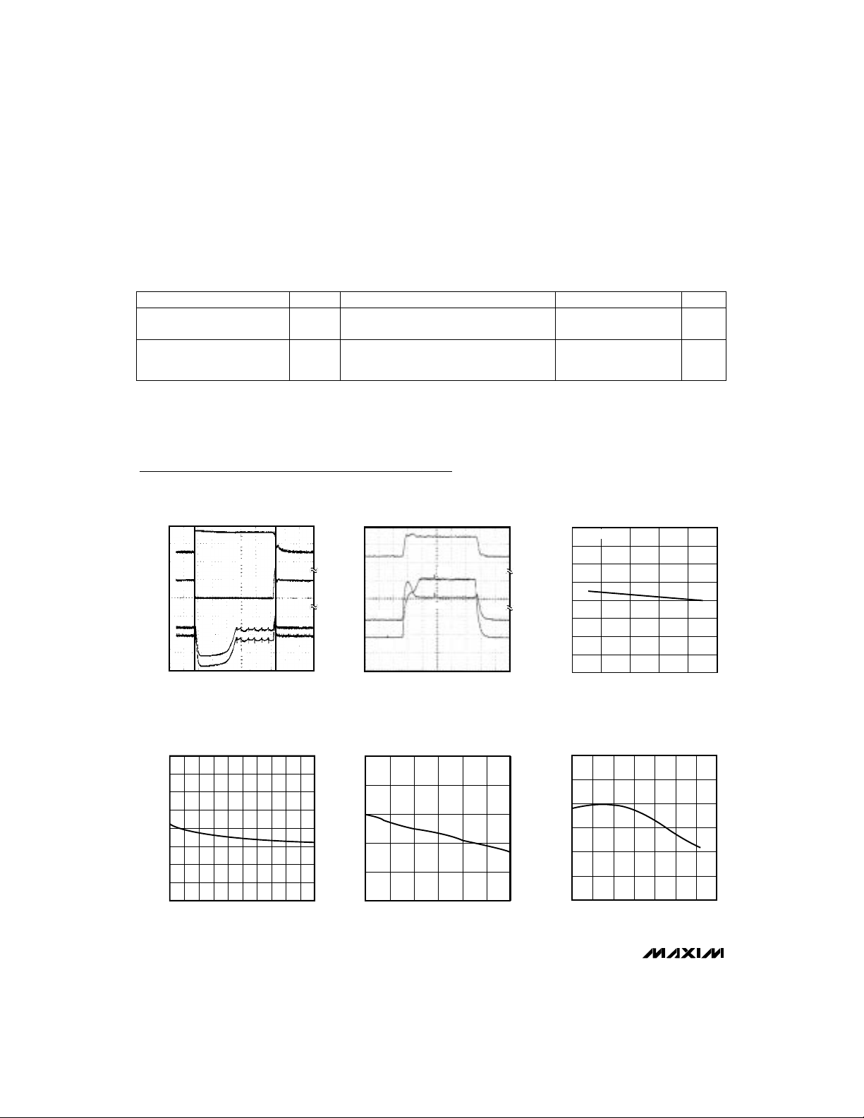
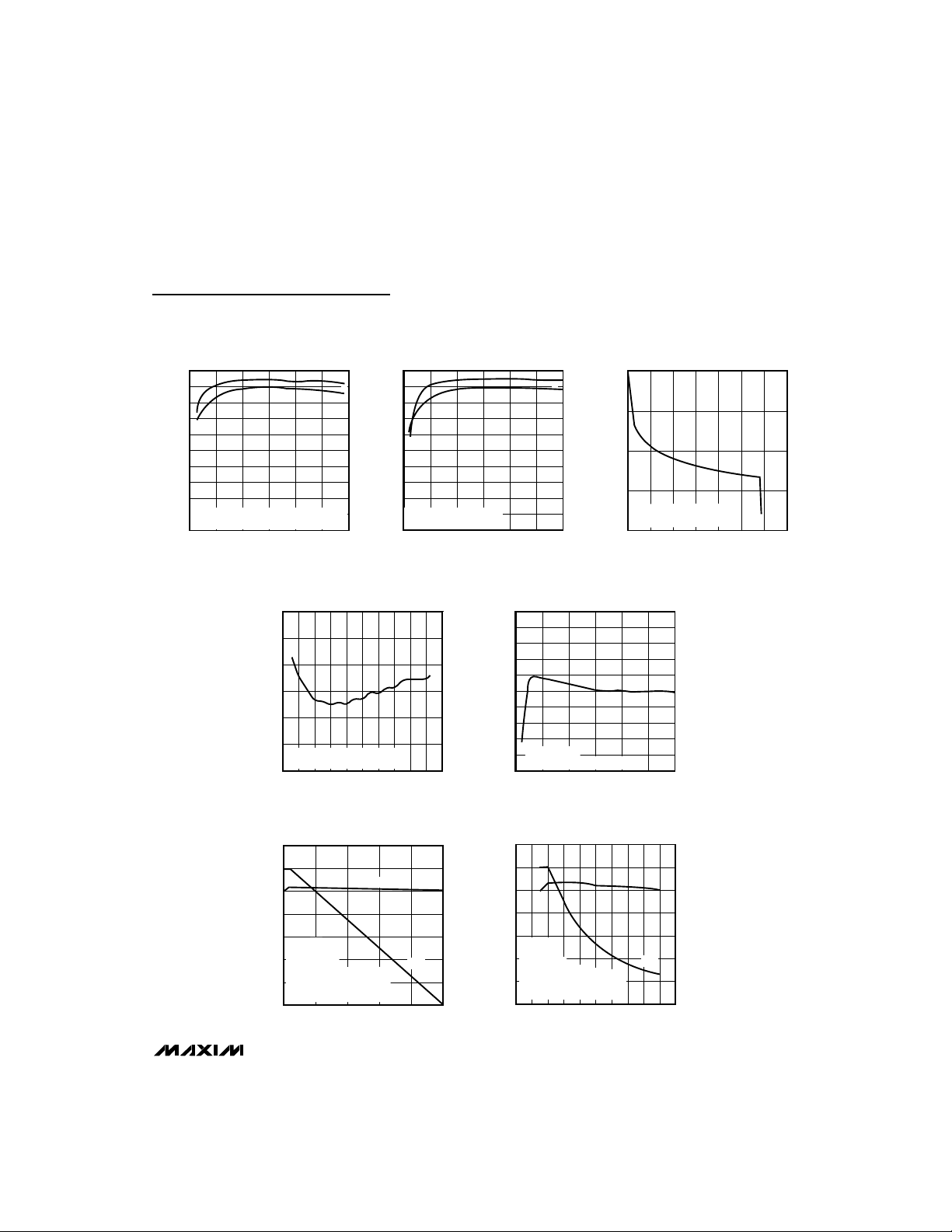
Typical Operating Characteristics
(Circuit of Figure 1, V
DCIN
= 20V, TA = +25°C, unless otherwise noted.)
LOAD-TRANSIENT RESPONSE
(BATTERY REMOVAL AND REINSERTION)
MAX1645 toc01
ChargingVoltage() = 15000mV
ChargingCurrent() = 1000mA
CCI
CCI
CCI
16V
14V
12V
1A
0
1.5V
V
CCV
/V
CCI
I
BATT
V
BATT
1V
0.5V
2ms/div
CCV
CCV
CCV
BATTERY REMOVED BATTERY INSERTED
LOAD-TRANSIENT RESPONSE
(STEP IN LOAD CURRENT)
MAX1645 toc02
ChargingCurrent() = 3008mA
V
BATT
= 16V
LOAD STEP: 0A TO 2A
I
SOURCE
LIMIT = 2.5A
CCS
CCS
CCS
4A
2A
0
2A
1V
0
1ms/div
CCI
CCI
CCI
V
CCV
/V
CCI
I
BATT
V
BATT
5.20
5.25
5.30
5.35
5.40
5.45
5.50
5.55
5.60
5 1015202530
LDO LINE REGULATION
MAX1645 toc03
V
DCIN
(V)
V
LDO
(V)
I
LOAD
= 0
4.080
4.090
4.085
4.100
4.095
4.105
4.110
-40 20 40-20 0 60 80 100
REFERENCE VOLTAGE
vs. TEMPERATURE
MAX1645 toc06
TEMPERATURE (°C)
V
REF
(V)
ELECTRICAL CHARACTERISTICS (continued)
(Circuit of Figure 1, VDD= +3.3V, V
BATT
= +16.8V, V
DCIN
= +18V, TA= -40°C to +85°C, unless otherwise noted. Guaranteed by design.)
Note 1: Guaranteed by meeting the SMB timing specs.
Note 2: The charger reverts to a trickle-charge mode of I
CHARGE
= 128mA below this threshold.
Note 3: Does not include current-sense resistor tolerance.
Note 4: Voltage difference between CCV, and CCI or CCS when one of these three pins is held low and the others try to pull high.
Maximum Charge Period
Without a ChargingVoltage() or
Charging Current() loaded
t
WDT
140 210
sec
SDA Output Data Valid
from SCL
t
DV
1
µs
PARAMETER SYMBOL MIN MAX UNITSCONDITIONS
Page 9
MAX1645
Advanced Chemistry-Independent, Level 2
Battery Charger with Input Current Limiting
_______________________________________________________________________________________
9
Typical Operating Characteristics (continued)
(Circuit of Figure 1, V
DCIN
= 20V, TA = +25°C, unless otherwise noted.)
EFFICIENCY vs. BATTERY CURRENT
(VOLTAGE-CONTROL LOOP)
100
95
90
85
80
75
70
EFFICIENCY (%)
65
60
A: V
= 20V, ChargingVoltage() = 16.8V
DCIN
55
= 16V, ChargingVoltage() = 8.4V
B: V
DCIN
50
0 1000500 1500 2000 2500 3000
BATTERY CURRENT (mA)
A
B
MAX1645 toc07
EFFICIENCY vs. BATTERY CURRENT
(CURRENT-CONTROL LOOP)
100
95
90
85
80
75
70
EFFICIENCY (%)
65
60
A: V
= 20V, V
DCIN
55
B: V
DCIN
50
0 1000500 1500 2000 2500 3000
= 16.8V
BATT
= 16V, V
= 8.4V
BATT
ChargingCurrent() (CODE)
A
B
0.001
MAX1645 toc08
0.01
0.1
1.0
DROP IN BATT OUTPUT VOLTAGE (%)
10
OUTPUT VI CHARACTERISTICS
ChargingVoltage() = 16,800mV
ChargingCurrent() = 3008mA
0 1500 2000500 1000 2500 3000 3500
LOAD CURRENT (mA)
MAX1645 toc09
BATT VOLTAGE ERROR
vs. ChargingVoltage() CODE
0.3
0.2
0.1
0
-0.1
BATT VOLTAGE ERROR (%)
-0.2
I
= 0
BATT
MEASURED AT AVAILABLE CODES
-0.3
0000 80004000 12000 16000 20000
ChargingVoltage() (CODE)
SOURCE/BATT CURRENT vs. LOAD CURRENT
WITH SOURCE CURRENT LIMIT
3.5
3.0
2.5
2.0
1.5
V
= 2V
CLS
= 40mΩ
R
CSS
1.0
V
SOURCE/BATT CURRENT (A)
= 16.8V
BATT
SOURCE CURRENT LIMIT = 2.5A
0.5
ChargingCurrent() = 3008mA
ChargingVoltage() = 18,432mV
0
0 1.00.5 1.5 2.0 2.5
I
IN
LOAD CURRENT (A)
I
BATT
MAX1645 toc10
MAX1645 toc12
CURRENT-SETTING ERROR
vs. ChargingCurrent() CODE
5
4
3
2
1
0
-1
-2
BATT CURRENT ERROR (%)
-3
V
= 12.6V
BATT
-4
MEASURED AT AVAILABLE CODES
-5
0 1000500 1500 2000 2500 3000
ChargingCurrent() (CODE)
SOURCE/BATT CURRENT vs. V
WITH SOURCE CURRENT LIMIT
3.5
3.0
2.5
2.0
1.5
I
= 2A
LOAD
= 2V
V
CLS
1.0
= 40mΩ
R
SOURCE/BATT CURRENT (A)
CSS
ChargingVoltage() = 18,432mV
0.5
ChargingCurrent() = 3008mA
SOURCE CURRENT LIMIT = 2.5A
0
042 6 8101214161820
I
IN
V
(V)
BATT
MAX1645 toc11
BATT
MAX1645 toc13
I
BATT
Page 10
MAX1645
Advanced Chemistry-Independent, Level 2
Battery Charger with Input Current Limiting
10 ______________________________________________________________________________________
Pin Description
Battery Voltage OutputBATT9
DAC Voltage Output DAC10
Logic Circuitry Supply Voltage Input (2.8V to 5.65V) V
DD
11
Thermistor Voltage Input THM12
SMB Clock Input SCL13
Charging Source Compensation Capacitor Connection. Connect a 0.01µF capacitor from CCS to GND.CCS5
Battery Current-Loop Compensation Capacitor Connection. Connect a 0.01µF capacitor from CCI to GND. CCI6
Battery Voltage-Loop Compensation Capacitor Connection. Connect a 10kΩ resistor in series with a 0.01µF
capacitor to GND.
CCV7
Ground GND8
4.096V Reference Voltage OutputREF4
Source Current Limit InputCLS3
PIN
5.4V Linear-Regulator Voltage Output. Bypass with a 1µF capacitor to GND.LDO2
DC Supply Voltage InputDCIN1
FUNCTIONNAME
Inductor Voltage Sense InputLX22
High-Side NMOS Driver OutputDHI23
High-Side Driver Bootstrap Voltage Input. Bypass with 0.1µF capacitor to LX.BST24
Charging Source Current-Sense Negative InputCSSN25
Charging Source Current-Sense Positive InputCSSP26
Battery Current-Sense Positive InputCSIP18
Power GroundPGND19
Low-Side NMOS Driver OutputDLO20
Low-Side NMOS Driver Supply Voltage. Bypass with 0.1µF capacitor to GND.DLOV21
Battery Current-Sense Negative InputCSIN17
PMOS Load Switch Driver OutputPDL16
Interrupt Output. Open-drain output. Needs external pull-up.
INT
15
SMB Data Input/Output. Open-drain output. Needs external pull-up.SDA14
Charging Source PMOS Switch Driver OutputPDS27
Charging Source Voltage InputCVS28
Page 11

MAX1645
Advanced Chemistry-Independent, Level 2
Battery Charger with Input Current Limiting
______________________________________________________________________________________ 11
Detailed Description
The MAX1645 consists of current-sense amplifiers, an
SMBus interface, transconductance amplifiers, reference circuitry, and a DC–DC converter (Figure 2). The
DC–DC converter generates the control signals for the
external MOSFETs to maintain the voltage and the current set by the SMBus interface. The MAX1645 features
a voltage-regulation loop and two current-regulation
loops. The loops operate independently of each other.
The voltage-regulation loop monitors BATT to ensure
that its voltage never exceeds the voltage set point
(V0). The battery current-regulation loop monitors current delivered to BATT to ensure that it never exceeds
the current-limit set point (I0). The battery current-regulation loop is in control as long as BATT voltage is
below V0. When BATT voltage reaches V0, the current
loop no longer regulates. A third loop reduces the battery-charging current when the sum of the system (the
main load) and the battery charger input current
exceeds the charging source current limit.
Setting Output Voltage
The MAX1645’s voltage DAC has a 16mV LSB and an
18.432V full scale. The SMBus specification allows for a
16-bit ChargingVoltage() command that translates to a
1mV LSB and a 65.535V full-scale voltage; therefore,
the ChargingVoltage() value corresponds to the output
voltage in millivolts. The MAX1645 ignores the first four
LSBs and uses the next 11 LSBs to control the voltage
DAC. All codes greater than or equal to 0b0100 1000
0000 0000 (18432mV) result in a voltage overrange,
limiting the charger voltage to 18.432V. All codes below
0b0000 0100 0000 0000 (1024mV) terminate charging.
Setting Output Current
The MAX1645’s current DAC has a 64mA LSB and a
3.008A full scale. The SMBus specification allows for a
16-bit ChargingCurrent() command that translates to a
1mA LSB and a 65.535A full-scale current; the
ChargingCurrent() value corresponds to the charging
voltage in milliamps. The MAX1645 drops the first six
LSBs and uses the next six LSBs to control the current
DAC. All codes above 0b00 1011 1100 0000 (3008mA)
result in a current overrange, limiting the charger current to 3.008A. All codes below 0b0000 0000 1000
0000 (128mA) turn the charging current off. A 50mΩ
sense resistor (R2 in Figure 1) is required to achieve
the correct CODE/current scaling.
Input Current Limiting
The MAX1645 limits the current drawn by the charger
when the load current becomes high. The device limits
the charging current so the AC adapter voltage is not
loaded down. An internal amplifier compares the voltage between CSSP and CSSN to the voltage at CLS/20.
V
CLS
is set by a resistor divider between REF and
GND.
The input source current is the sum of the device cur-
rent, the charge input current, and the load current. The
device current is minimal (6mA max) in comparison to
the charge and load currents. The charger input current is generated by the DC-DC converter; therefore, the
actual source current required is determined as follows:
I
SOURCE
= I
LOAD
+ [(I
CHARGE
· V
BATT)
/ (VIN· η)]
where η is the efficiency of the DC-DC converter (typically 85% to 95%).
V
CLS
determines the threshold voltage of the CSS comparator. R3 and R4 (Figure 1) set the voltage at CLS.
Sense resistor R1 sets the maximum allowable source
current. Calculate the maximum current as follows:
I
MAX
= V
CLS
/ (20 · R1)
(Limit V
CSSP
- V
CSSN
to between 102.4mV and
204.8mV.)
The configuration in Figure 1 provides an input current
limit of:
I
MAX
= (2.048V / 20) / 0.04Ω = 2.56A
LDO Regulator
The LDO provides a +5.4V supply derived from DCIN
and can deliver up to 15mA of current. The LDO sets
the gate-drive level of the NMOS switches in the
DC-DC converter. The drivers are actually powered by
DLOV and BST, which must be connected to LDO
through a lowpass filter and a diode as shown in Figure
1. See also the
MOSFET Drivers
section. The LDO also
supplies the 4.096V reference and most of the control
circuitry. Bypass LDO with a 1µF capacitor.
VDDSupply
This input provides power to the SMBus interface and
the thermistor comparators. Typically connect VDDto
LDO or, to keep the SMBus interface of the MAX1645
active while the supply to DCIN is removed, connect an
external supply to VDD.
Page 12

MAX1645
Advanced Chemistry-Independent, Level 2
Battery Charger with Input Current Limiting
12 ______________________________________________________________________________________
ADAPTER IN
Figure 1. Typical Application Circuit
R5
10k
C11
0.01µF
R13
1k
C23
0.1µF
R3
100k
R4
100k
C10
0.01µF
CVS
DCIN
REF
CLS
GND
DAC
CCV
CCI
CCS
MAX1645
CSSP
CSSN
LDO
DLOV
PGND
CSIP
CSIN
PDL
BATT
THM
SCL
SDA
PDS
BST
DLO
V
P1
FDS6675 D1
R14
4.7Ω
C20, 1µF
C19, 1µF
4.7Ω
C6
1µF
DHI
N1
FDS6680
LX
N2
FDS6612A
DD
INT
C12
1µF
C18
0.1µF
R7
10k
C13
1.5nF
C24
0.1µF
R10
10k
1N5821
R15
C14
0.1µF
D2
R11
R16
1Ω
1N5821
R1
0.04Ω
R12
33Ω
D3
1N4148
C16
0.1µF
L1
22µH
1Ω
R2
0.05Ω
R6
10k
R8
10k
R9
10k
D4
1N4148
C5
1µF
C7
1µF
C8
0.1µF
C9
0.01µF
22µF
C1
FDS6675
C2
22µF
LOAD
P2
BATTERY
HOST
C4
22µF
C3
22µF
Page 13

MAX1645
Advanced Chemistry-Independent, Level 2
Battery Charger with Input Current Limiting
______________________________________________________________________________________ 13
Figure 2. Functional Diagram
CSSP
CSSN
CLS
CSIP
CSIN
CSS
GMS
CSI
GMI
BATT
GMV
MAX1645
LVC
DHI
DC-DC
DLO
BST
DHI
LX
DLOV
DLO
PGND
CCS
CCI
CCV
CVS
BATT
V
DD
SCL
SDA
INT
THM
SMB
TEMP
DACI
DACV
PDL
VL
REF
PDS
PDS
PDL
DCIN
LDO
REF
GND
DAC
Page 14

MAX1645
Advanced Chemistry-Independent, Level 2
Battery Charger with Input Current Limiting
14 ______________________________________________________________________________________
Operating Conditions
The MAX1645 changes its operation depending on the
voltages at DCIN, BATT, V
DD,
and THM. Several impor-
tant operating states follow:
• AC Present. When DCIN is > 7.5V, the battery is
considered to be in an AC Present state. In this condition, both the LDO and REF will function properly
and battery charging is allowed. When AC is present, the AC_PRESENT bit (bit 15) in the
ChargerStatus() register is set to “1.”
• Power Fail. When DCIN is < BATT + 0.3V, the
MAX1645 is in the Power Fail state, since the charger
doesn’t have enough input voltage to charge the battery. In Power Fail, the PDS input PMOS switch is
turned off and the POWER_FAIL bit (bit 13) in the
ChargerStatus() register is set to “1.”
• Battery Present. When THM is < 91% of VDD, the
battery is considered to be present. The MAX1645
uses the THM pin to detect when a battery is connected to the charger. When the battery is present,
the BATTERY_PRESENT bit (bit 14) in the
ChargerStatus() register is set to “1” and charging
can proceed. When the battery is not present, all of
the MAX1645 registers are reset. With no battery present, the charger will still try to regulate the BATT pin
voltage at 18.432V with 128mA of current compliance.
• Battery Undervoltage. When BATT < 2.5V, the bat-
tery is in an undervoltage state. This causes the
charger to reduce its current compliance to 128mA.
The content of the ChargingCurrent() register is unaffected and, when the BATT voltage exceeds 2.7V,
normal charging resumes. ChargingVoltage() is unaffected and can be set as low as 1.024V.
• VDDUndervoltage. When VDD< 2.5V, the VDDsupply is in an undervoltage state, and the SMBus interface will not respond to commands. Coming out of
the undervoltage condition, MAX1645 will be in its
Power-On Reset state. No charging will occur when
VDDis under voltage.
SMBus Interface
The MAX1645 receives control inputs from the SMBus
interface. The serial interface complies with the SMBus
specification (refer to the System Management Bus
Specification from Intel Corporation). Charger functionality complies with the Intel/Duracell Smart Charger
Specification for a Level 2 charger.
The MAX1645 uses the SMBus Read-Word and WriteWord protocols to communicate with the battery being
charged, as well as with any host system that monitors
the battery-to-charger communications as a Level 2
SMBus charger. The MAX1645 is an SMBus slave
device and does not initiate communication on the bus.
It receives commands and responds to queries for status information. Figure 3 shows examples of the SMBus
Write-Word and Read-Word protocols, and Figures 4
and 5 show the SMBus serial-interface timing.
Each communication with the MAX1645 begins with the
MASTER issuing a START condition that is defined as a
falling edge on SDA with SCL high and ends with a
STOP condition defined as a rising edge on SDA with
SCL high. Between the START and STOP conditions,
the device address, the command byte, and the data
bytes are sent. The MAX1645 device address is 0x12
and supports the charger commands as described in
Tables 1–6.
Battery Charger Commands
ChargerSpecInfo()
The ChargerSpecInfo() command uses the Read-Word
protocol (Figure 3b). The command code for
ChargerSpecInfo() is 0x11 (0b00010001). Table 1 lists
the functions of the data bits (D0–D15). Bit 0 refers to
the D0 bit in the Read-Word protocol. The MAX1645 is
version 1.0; therefore, the ChargerSpecInfo() command
returns 0x01.
ChargerMode()
The ChargerMode() command uses the Write-Word
protocol (Figure 3a). The command code for
ChargerMode() is 0x12 (0b00010010). Table 2 lists the
functions of the data bits (D0–D15). Bit 0 refers to the
D0 bit in the Write-Word protocol.
To charge a battery that has a thermistor impedance in
the HOT range (i.e., THERMISTOR_HOT = 1 and THERMISTOR_UR = 0), the host must use the Charger
Mode() command to clear HOT_STOP after the battery
is inserted. The HOT_STOP bit returns to its default
power-up condition (“1”) whenever the battery is
removed.
ChargerStatus()
The ChargerStatus() command uses the Read-Word
protocol (Figure 3b). The command code for Charger
Status() is 0x13 (0b00010011). Table 3 describes the
functions of the data bits (D0–D15). Bit 0 refers to the
D0 bit in the Read-Word protocol.
The ChargerStatus() command returns information
about thermistor impedance and the MAX1645’s internal state. The latched bits, THERMISTOR_HOT and
ALARM_INHIBITED, are cleared whenever BATTERY_
PRESENT = 0 or ChargerMode() is written with
POR_RESET = 1. The ALARM_INHIBITED status bit can
also be cleared by writing a new charging current OR
charging voltage.
Page 15

MAX1645
______________________________________________________________________________________ 15
Advanced Chemistry-Independent, Level 2
Battery Charger with Input Current Limiting
Figure 3. SMBus a) Write-Word and b) Read-Word Protocols
Preset to
0b0001001
D7 D0 D15 D8
ChargerMode() = 0x12
ChargingCurrent() = 0x14
ChargerVoltage() = 0x15
AlarmWarning() = 0x16
Preset to
0b0001001
Preset to
0b0001001
D7 D0 D15 D8
ChargerSpecInfo() =
0x11
ChargerStatus() =
0x13
0
1b
ACK
0MSB LSB
1b8 bits
ACK
COMMAND
BYTE
0MSB LSB
1b7 bits
W
SLAVE
ADDRESS
S
0MSB LSB
1b8 bits
ACK
LOW
DATA
BYTE
P
0MSB LSB
1b8 bits
ACK
HIGH
DATA
BYTE
a) Write-Word Format
b) Read-Word Format
Legend:
S = Start Condition or Repeated Start Condition P = Stop Condition
ACK = Acknowledge (logic low) NACK = NOT Acknowledge (logic high)
W = Write Bit (logic low) R = Read Bit (logic high)
MASTER TO SLAVE
SLAVE TO MASTER
HIGH
DATA
BYTE
NACK
8 bits 1b
MSB LSB 1
P
LOW
DATA
BYTE
ACK
8 bits 1b
MSB LSB 0
SLAVE
ADDRESS
R
7 bits 1b
MSB LSB 1
ACK
1b
0
COMMAND
BYTE
ACK
8 bits 1b
MSB LSB 0
SACK
1b
0
S
SLAVE
ADDRESS
W
7 bits 1b
MSB LSB 0
Page 16

MAX1645
Advanced Chemistry-Independent, Level 2
Battery Charger with Input Current Limiting
16 ______________________________________________________________________________________
MOST SIGNIFICANT
Figure 4. SMBus Serial Interface Timing—Address
Figure 5. SMBus Serial Interface Timing—Acknowledgment
START
CONDITION
ADDRESS BIT (A6)
CLOCKED INTO SLAVE
A5 CLOCKED
INTO SLAVE
A4 CLOCKED
INTO SLAVE
SCL
A3 CLOCKED
INTO SLAVE
SDA
t
SU:STA
SCL
SDA
t
HD:STA
t
SU:DAT
INTO SLAVE
R/W BIT
CLOCKED
t
HD:DAT
t
LOW
t
DV
ACKNOWLEDGE
BIT CLOCKED
INTO MASTER
SLAVE PULLING
SDA LOW
t
SU:DAT
MOST SIGNIFICANT BIT
OF DATA CLOCKED
INTO MASTER
t
DV
t
HD:DAT
t
HIGH
Page 17

MAX1645
Advanced Chemistry-Independent, Level 2
Battery Charger with Input Current Limiting
______________________________________________________________________________________ 17
Returns a “0”Reserved8
Returns a “0”Reserved9
Returns a “0”Reserved10
Returns a “0”Reserved11
Returns a “0”Reserved12
Returns a “0,” indicating no smart battery selector functionalitySELECTOR_SUPPORT4
Returns a “0”Reserved5
Returns a “0”Reserved6
Returns a “0”Reserved7
Returns a “0” for Version 1.0CHARGER_SPEC3
Returns a “0” for Version 1.0CHARGER_SPEC2
BIT
Returns a “0” for Version 1.0CHARGER_SPEC1
Returns a “1” for Version 1.0CHARGER_SPEC0
DESCRIPTIONNAME
Returns a “0”Reserved15
Returns a “0”Reserved14
Returns a “0”Reserved13
Table 1. ChargerSpecInfo()
Command: 0x11
Page 18

MAX1645
Advanced Chemistry-Independent, Level 2
Battery Charger with Input Current Limiting
18 ______________________________________________________________________________________
Table 2. ChargerMode()
Command: 0x12
*State at chip initial power-on (i.e., V
DD
from 0 to +3.3V)
13 Not implemented
14 Not implemented
15 Not implemented
NAME DESCRIPTION
0 INHIBIT_CHARGE
0* = Allow normal operation; clear the CHG_INHIBITED flip-flop.
1 = Turn off the charger; set the CHG_INHIBITED flip-flop.
The CHG_INHIBITED flip-flop is not affected by any other commands.
1 ENABLE_POLLING Not implemented
BIT
2 POR_RESET
0 = No change.
1 = Change the ChargingVoltage() to 0xFFFF and the ChargingCurrent()
to 0x00C0; clear the THERMISTOR_HOT and ALARM_INHIBITED flipflops.
3 RESET_TO_ZERO Not implemented
7 Not implemented
6 POWER_FAIL_MASK
0* = Interrupt on either edge of the POWER_FAIL status bit.
1 = Do not interrupt because of a POWER_FAIL bit change.
5 BATTERY_PRESENT_ MASK
0* = Interrupt on either edge of the BATTERY_PRESENT status bit.
1 = Do not interrupt because of a BATTERY_PRESENT bit change.
4 AC_PRESENT_MASK
0* = Interrupt on either edge of the AC_PRESENT status bit.
1 = Do not interrupt because of an AC_PRESENT bit change.
12 Not implemented
11 Not implemented
10 HOT_STOP
0 = The THERMISTOR_HOT status bit does not turn off the charger.
1* = The THERMISTOR_HOT status bit does turn off the charger.
THERMISTOR_HOT is reset by either POR_RESET or
BATTERY_PRESENT = 0 status bit.
9 Not implemented
8 Not implemented
Page 19

MAX1645
Advanced Chemistry-Independent, Level 2
Battery Charger with Input Current Limiting
______________________________________________________________________________________ 19
NAME FUNCTION
0 CHARGE_INHIBITED
0* = Ready to charge Smart Battery.
1 = Charger is inhibited, I(chg) = 0mA.
This status bit returns the value of the CHG_INHIBITED flip-flop.
1 MASTER_MODE Always returns “0”
BIT
2 VOLTAGE_NOT_REG
0 = Battery voltage is limited at the set point.
1 = Battery voltage is less than the set point.
3 CURRENT_NOT_REG
0 = Battery current is limited at the set point.
1 = Battery current is less than the set point.
7 VOLTAGE_OR
0 = The ChargingVoltage() value is valid for the MAX1645.
1* = The ChargingVoltage() value exceeds the MAX1645 output range, i.e.,
programmed ChargingVoltage() exceeds 1843mV.
6 CURRENT_OR
0* = The ChargingCurrent() value is valid for the MAX1645.
1 = The ChargingCurrent() value exceeds the MAX1645 output range, i.e.,
programmed ChargingCurrent() exceeds 3008mA.
5 LEVEL_3 Always returns a “0”
4 LEVEL_2 Always returns a “1”
12 ALARM_INHIBITED
Returns the state of the ALARM_INHIBITED flip-flop. This flip-flop is set by either a
watchdog timeout or by writing an AlarmWarning() command with bits 11, 12, 13, 14,
or 15 set. This flip-flop is cleared by BATTERY_PRESENT = 0, writing a “1” into the
POR_RESET bit in the ChargerMode() command, or by receiving successive
ChargingVoltage() and ChargingCurrent() commands. POR: 0.
11 THERMISTOR_UR
0 = THM is > 7.5% of the reference voltage.
1 = THM is < 7.5% of the reference voltage.
10 THERMISTOR_HOT
0 = THM has not dropped to < 23.5% of the reference voltage.
1 = THM has dropped to < 23.5% of the reference voltage.
THERMISTOR_HOT flip-flop cleared by BATTERY_PRESENT = 0 or writing a “1” into
the POR_RESET bit in the ChargerMode() command.
9 THERMISTOR_COLD
0 = THM is < 75.5% of the reference voltage.
1 = THM is > 75.5% of the reference voltage.
8 THERMISTOR_OR
0 = THM is < 91% of the reference voltage.
1 = THM is > 91% of the reference voltage.
Table 3. ChargerStatus()
15 AC_PRESENT
0 = DCIN is below the 7.5V undervoltage threshold.
1 = DCIN is above the 7.5V undervoltage threshold.
14 BATTERY_PRESENT
0 = No battery is present (based on THM input).
1 = Battery is present (based on THM input).
13 POWER_FAIL
0 = The charging source voltage CVS is above the BATT voltage.
1 = The charging source voltage CVS is below the BATT voltage.
Command: 0x13
*State at chip initial power-on.
Page 20

MAX1645
Advanced Chemistry-Independent, Level 2
Battery Charger with Input Current Limiting
20 ______________________________________________________________________________________
Table 4. ChargerCurrent()
Command: 0x14
NAME FUNCTION
0 Not used. Normally a 1mA weight.
1 Not used. Normally a 2mA weight.
BIT
2 Not used. Normally a 4mA weight.
3 Not used. Normally an 8mA weight.
7 Charge Current, DACI 1
0 = Adds 0mA of charger-current compliance.
1 = Adds 128mA of charger-current compliance.
6 Charge Current, DACI 0
0 = Adds 0mA of charger-current compliance.
1 = Adds 64mA of charger-current compliance, 128mA min.
5 Not used. Normally a 32mA weight.
4 Not used. Normally a 16mA weight.
12–15
0 = Adds 0mA of charger current compliance.
1 = Sets charger compliance into overrange, 3008mA.
11 Charge Current, DACI 5
0 = Adds 0mA of charger-current compliance.
1 = Adds 2048mA of charger-current compliance, 3008mA max.
10 Charge Current, DACI 4
0 = Adds 0mA of charger-current compliance.
1 = Adds 1024mA of charger-current compliance.
9 Charge Current, DACI 3
0 = Adds 0mA of charger-current compliance.
1 = Adds 512mA of charger-current compliance.
8 Charge Current, DACI 2
0 = Adds 0mA of charger-current compliance.
1 = Adds 256mA of charger-current compliance.
Page 21

MAX1645
Advanced Chemistry-Independent, Level 2
Battery Charger with Input Current Limiting
______________________________________________________________________________________ 21
Table 5. ChargingVoltage()
Command: 0x15
BIT NAME FUNCTION
0 Not used. Normally a 1mV weight.
1 Not used. Normally a 2mV weight.
PIN
2 Not used. Normally a 4mV weight.
3 Not used. Normally an 8mV weight.
7 Charge Voltage, DACV 3
0 = Adds 0mV of charger-voltage compliance.
1 = Adds 128mV of charger-voltage compliance, 1.024V min.
6 Charge Voltage, DACV 2
0 = Adds 0mV of charger-voltage compliance.
1 = Adds 64mV of charger-voltage compliance, 1.024V min.
5 Charge Voltage, DACV 1
0 = Adds 0mV of charger-voltage compliance.
1 = Adds 32mV of charger-voltage compliance, 1.024V min.
4 Charge Voltage, DACV 0
0 = Adds 0mV of charger-voltage compliance.
1 = Adds 16mV of charger-voltage compliance, 1.024V min.
12 Charge Voltage, DACV 8
0 = Adds 0mV of charger-voltage compliance.
1 = Adds 4096mV of charger-voltage compliance.
11 Charge Voltage, DACV 7
0 = Adds 0mV of charger-voltage compliance.
1 = Adds 2048mV of charger-voltage compliance.
10 Charge Voltage, DACV 6
0 = Adds 0mA of charger-voltage compliance.
1 = Adds 1024mV of charger-voltage compliance.
9 Charge Voltage, DACV 5
0 = Adds 0mV of charger-voltage compliance.
1 = Adds 512mV of charger-voltage compliance, 1.024V min.
8 Charge Voltage, DACV 4
0 = Adds 0mV of charger-voltage compliance.
1 = Adds 256mV of charger-voltage compliance, 1.024V min.
13 Charge Voltage, DACV 9
0 = Adds 0mV of charger-voltage compliance.
1 = Adds 8192mV of charger-voltage compliance.
14 Charge Voltage, DACV 10
0 = Adds 0mV of charger-voltage compliance.
1 = Adds 16384mV of charger-voltage compliance, 18432mV max.
15 Charge Voltage, Overrange
0 = Adds 0mV of charger-voltage compliance.
1 = Sets charger compliance into overrange, 18432mV.
Page 22

MAX1645
Advanced Chemistry-Independent, Level 2
Battery Charger with Input Current Limiting
22 ______________________________________________________________________________________
Table 6. AlarmWarning()
Command: 0x16
13 OTHER_ALARM
0 = Charge normally
1 = Terminate charging
14
TERMINATE_CHARGE_ ALARM
0 = Charge normally
1 = Terminate charging
15 OVER_CHARGE_ALARM
0 = Charge normally
1 = Terminate charging
BIT NAME DESCRIPTION
0 Error Code Not used
1 Error Code Not used
BIT
2 Error Code Not used
3 Error Code Not used
7 INITIALIZING Not used
6 DISCHARGING Not used
5 FULLY_CHARGED Not used
4 FULLY_DISCHARGED Not used
12 OVER_TEMP_ALARM
0 = Charge normally
1 = Terminate charging
11 TERMINATE_ DISCHARGE_ALARM
0 = Charge normally
1 = Terminate charging
10 Reserved Not used
9 REMAINING_CAPACITY_ ALARM Not used
8 REMAINING_TIME_ ALARM Not used
Page 23

MAX1645
Advanced Chemistry-Independent, Level 2
Battery Charger with Input Current Limiting
______________________________________________________________________________________ 23
ChargingCurrent() (POR: 0x0080)
The ChargingCurrent() command uses the Write-Word
protocol (Figure 3a). The command code for ChargingCurrent() is 0x14 (0b00010100). The 16-bit binary number formed by D15–D0 represents the current-limit set
point (I0) in milliamps. However, since the MAX1645 has
64mA resolution in setting I0, the D0–D5 bits are
ignored as shown in Table 4. Figure 6 shows the mapping between I0 (the current-regulation-loop set point)
and the ChargingCurrent() code. All codes above 0b00
1011 1100 0000 (3008mA) result in a current overrange,
limiting the charger current to 3.008A. All codes below
0b0000 0000 1000 0000 (128mA) turn the charging current off. A 50mΩ sense resistor (R2 in Figure 1) is
required to achieve the correct CODE/current scaling.
The power-on reset value for the ChargingCurrent() register is 0x0080; thus, the first time a MAX1645 is powered on, the BATT current regulates to 128mA. Any time
the battery is removed, the ChargingCurrent() register
returns to its power-on reset state.
ChargingVoltage() (POR: 0x4800)
The ChargingVoltage() command uses the Write-Word
protocol (Figure 3a). The command code for
ChargingVoltage() is 0x15 (0b00010101). The 16-bit
binary number formed by D15–D0 represents the voltage set point (V0) in millivolts; however, since the
MAX1645 has 16mV resolution in setting V0, the D0, D1,
D2, and D3 bits are ignored as shown in Table 5.
The ChargingVoltage command is used to set the battery charging voltage compliance from 1.024V to
18.432V. All codes greater than or equal to 0b0100
1000 0000 0000 (18432mV) result in a voltage overrange, limiting the charger voltage to 18.432V. All codes
below 0b0000 0100 0000 0000 (1024mV) terminate
charge. Figure 7 shows the mapping between V0
(the voltage-regulation-loop set point) and the
ChargingVoltage() code.
The power-on reset value for the ChargingVoltage() register is 0x4880; thus, the first time a MAX1645 is powered on, the BATT voltage regulates to 18.432V. Any
time the battery is removed, the ChargingVoltage() register returns to its power-on reset state. The voltage at
DAC corresponds to the set compliance voltage divided
by 4.5.
AlarmWarning() (POR: Not Alarm)
The AlarmWarning() command uses the Write-Word
protocol (Figure 3a). The command code for
AlarmWarning() is 0x16 (0b00010110). AlarmWarning()
sets the ALARM_INHIBITED status bit in the MAX1645 if
D15, D14, D13, D12, or D11 of the Write-Word protocol
data equals 1. Table 6 summarizes the Alarm-
Warning() command’s function. The ALARM_INHIBITED
status bit remains set until the battery is removed, a
ChargerMode() command is written with the
POR_RESET bit set, or new ChargingCurrent() AND
ChargingVoltage() values are written. As long as
ALARM_INHIBITED = 1, the MAX1645 switching regulator remains off.
Interrupts and Alert Response Address
The MAX1645 requests an interrupt by pulling the INT
pin low. An interrupt is normally requested when there is
a change in the state of the ChargerStatus() bits
POWER_FAIL (bit 13), BATTERY_PRESENT (bit 14), or
AC_PRESENT (bit 15). Therefore, the INT pin will pull
low whenever the AC adapter is connected or disconnected, the battery is inserted or removed, or the charger goes in or out of dropout. The interrupts from each of
the ChargerStatus() bits can be masked by an associated ChargerMode() bit POWER_FAIL_MASK (bit 6), BATTERY_PRESENT_MASK (bit 5), or AC_PRESENT_MASK
(bit 4).
All interrupts are cleared by sending any command to
the MAX1645, or by sending a command to the
AlertResponse() address, 0x19, using a modified
Receive Byte protocol. In this protocol, all devices that
set an interrupt will try to respond by transmitting their
address, and the device with the highest priority, or
most leading 0’s, will be recognized and cleared. The
process will be repeated until all devices requesting
interrupts are addressed and cleared. The MAX1645
responds to the AlertResponse() address with 0x13,
which is its address and a trailing “1.”
Figure 6. Average Voltage Between CSIP and CSIN vs. Charging
Current() Code
150.4
102.4
51.2
IN CURRENT REGULATION (mV)
AVERAGE (CSIP-CSIN) VOLTAGE
6.4
0x0400
0x0080
128
1024
0x0800
2048 65535
0XFFFF
0x0BC0
3008
Page 24

MAX1645
Advanced Chemistry-Independent, Level 2
Battery Charger with Input Current Limiting
24 ______________________________________________________________________________________
Charger Timeout
The MAX1645 includes a timer that terminates charge if
the charger has not received a ChargingVoltage() or
ChargingCurrent() command in 175sec. During charging, the timer is reset each time a ChargingVoltage() or
ChargingCurrent() command is received; this ensures
that the charging cycle is not terminated.
If timeout occurs, charging will terminate and both
ChargingVoltage() and ChargingCurrent() commands
are required to restart charging. A power-on reset will
also restart charging at 128mA.
DC-to-DC Converter
The MAX1645 employs a buck regulator with a bootstrapped NMOS high-side switch and a low-side NMOS
synchronous rectifier.
DC-DC Controller
The control scheme is a constant off-time, variable frequency, cycle-by-cycle current mode. The off-time is
constant for a given BATT voltage; it varies with V
BATT
to keep the ripple current constant. During low-dropout
operation, a maximum on-time of 10ms allows the controller to achieve >99% duty cycle with continuous conduction. Figure 8 shows the controller functional
diagram.
MOSFET Drivers
The low-side driver output DLO swings from 0V to
DLOV. DLOV is usually connected through a filter to
LDO. The high-side driver output DHI is bootstrapped
off LX and swings from VLXto V
BST
. When the low-side
18.432V
Figure 7. ChargingVoltage() Code to Voltage Mapping
16.800V
= 4.096V
V
REF
VDCIN > 20V
12.592V
8.400V
VOLTAGE SET POINT (V0)
4.192V
1.024V
0
0x0400
0
0x20Dx 0x41A00x313x 0x48000x106x
ChargingVoltage() D15–D0 DATA
0xFFFF
Page 25

MAX1645
Advanced Chemistry-Independent, Level 2
Battery Charger with Input Current Limiting
______________________________________________________________________________________ 25
Figure 8. DC-to-DC Converter Functional Diagram
10ms
RESET
4.0V
0.25V
IMAX
CCMP
IMIN
S
BST
RQ
MAX1645
RQ
CHG
Q
S
1µs
CSSP ADAPTER IN
CSS
CSSN
BST
DHI
DHI
LX
DLO
DLO
R1
LDO
C
BST
L1
0.1V
ZCMP
CCVCCICCS
CONTROL
LVC
CSIP
CSI
GMS
GMI
GMV
DACV
DACI
ON
CLS
R
FC
70k
R
FI
20k
CSIN
BATT
C
OUT
R2
BATTERY
Page 26

MAX1645
Advanced Chemistry-Independent, Level 2
Battery Charger with Input Current Limiting
26 ______________________________________________________________________________________
driver turns on, BST rises to one diode voltage below
DLOV.
Filter DLOV with an RC circuit whose cutoff frequency
is about 50kHz. The configuration in Figure 1 introduces a cutoff frequency of around 48kHz.
f = 1 / 2πRC = 1 / (2 · π · 33Ω · 0.1µF) = 48kHz
Thermistor Comparators
Four thermistor comparators evaluate the voltage at the
THM input to determine the battery temperature. This
input is meant to be used with the internal thermistor
connected to ground inside the battery pack. Connect
the output of the battery thermistor to THM. Connect a
resistor from THM to VDD. The resistor-divider sets the
voltage at THM. When the charger is not powered up,
the battery temperature can still be determined if V
DD
is
powered from an external voltage source.
Thermistor Bits
Figure 9 shows the expected electrical behavior of a
103ETB-type thermistor (nominally 10kΩ at +25°C ±5%
or better) to be used with the MAX1645:
• THERMISTOR_OR bit is set when the thermistor
value is >100kΩ. This indicates that the thermistor is
open or a battery is not present. The charger is set to
POR, and the BATTERY_PRESENT bit is cleared.
• THERMISTOR_COLD bit is set when the thermistor
value is >30kΩ. The thermistor indicates a cold battery. This bit does not affect the charge.
• THERMISTOR_HOT bit is set when the thermistor
value is <3kΩ. This is a latched bit and is cleared by
removing the battery or sending a POR with the
ChargerMode() command. The charger is stopped
unless the HOT_STOP bit is cleared in the
ChargerMode() command.
• THERMISTOR_UR bit is set when the thermistor
value is <500Ω (i.e., THM is grounded).
Multiple bits may be set depending on the value of the
thermistor (e.g., a thermistor that is 450Ω will cause
both the THERMISTOR_HOT and the THERMISTOR_UR
bits to be set). The thermistor may be replaced by
fixed-value resistors in battery packs that do not require
the thermistor as a secondary fail-safe indicator. In this
case, it is the responsibility of the battery pack to
manipulate the resistance to obtain correct charger
behavior.
Load and Source Switch Drivers
The MAX1645 can drive two P-channel MOSFETs to
eliminate voltage drops across the Schottky diodes,
which are normally used to switch the load current from
the battery to the main DC source:
• The source switch P1 is controlled by PDS. This Pchannel MOSFET is turned on when CVS rises to
300mV above BATT and turns off when CVS falls to
100mV above BATT. The same signal that controls
the PDS also sets the POWER_FAIL bit in the
Charger Status() register. See
Operating Conditions
.
• The load switch P2 is controlled by PDL. This Pchannel MOSFET is turned off when the CVS rises to
100mV below BATT and turns on when CVS falls to
300mV below BATT.
Dropout Operation
The MAX1645 has a 99.99% duty-cycle capability with
a 10ms maximum on-time and 1µs off-time. This allows
the charger to achieve dropout performance limited
only by resistive losses in the DC-DC converter components (P1, R1, N1, R2; see Figure 1). The actual
dropout voltage is limited to 300mV between CVS and
BATT by the power-fail comparator (see
Operating
Conditions)
.
Figure 9. Typical Thermistor Characteristics
1000
100
10
RESISTANCE (kΩ)
1
0.1
-40
-50 -30 -20 -10 0 10 20 30 40 50 60 70 80 90 100 110
TEMPERATURE (°C)
Page 27

MAX1645
Advanced Chemistry-Independent, Level 2
Battery Charger with Input Current Limiting
______________________________________________________________________________________ 27
Applications Information
Smart Battery Charging
System/Background Information
A smart battery charging system, at a minimum, consists of a smart battery and smart battery charger compatible with the Smart Battery System Specifications
using the SMBus.
A system may use one or more smart batteries. Figure 10
shows a single-battery system. This configuration is
typically found in notebook computers, video cameras,
cellular phones, or other portable electronic equipment.
Another configuration uses two or more smart batteries
(Figure 11). The smart battery selector is used either to
connect batteries to the smart battery charger or the
system, or to disconnect them, as appropriate. For
each battery, three connections must be made: power
(the battery’s positive and negative terminals), the
SMBus (clock and data), and the safety signal (resistance, typically temperature dependent). Additionally,
the system host must be able to query any battery so it
can display the state of all batteries present in the system.
Figure 11 shows a two-battery system where battery 2
is being charged while battery 1 is powering the system. This configuration may be used to “condition” battery 1, allowing it to be fully discharged prior to
recharge.
Smart Battery Charger Types
Two types of smart battery chargers are defined: Level 2
and Level 3. All smart battery chargers communicate
with the smart battery using the SMBus; the two types
differ in their SMBus communication mode and whether
they modify the charging algorithm of the smart battery
(Table 7). Level 3 smart battery chargers are supersets
of Level 2 chargers and, as such, support all Level 2
charger commands.
V
Figure 10. Typical Single Smart Battery System
CC
+12V, -12V
SYSTEM
POWER
SUPPLY
DC (UNREGULATED) / V
BATTERY
SYSTEM
POWER
CONTROL
V
BATTERY
DC (UNREGULATED)
CONVERTER
(UNREGULATED)
AC
AC-DC
SYSTEM HOST
(SMBus HOST)
CRITICAL EVENTS
BATTERY DATA/STATUS REQUESTS
SMART
BATTERY
SAFETY
SIGNAL
CHARGING VOLTAGE/CURRENT
REQUESTS
CRITICAL EVENTS
MAX1645
SMART BATTERY
CHARGER
SMBus
Page 28

MAX1645
Advanced Chemistry-Independent, Level 2
Battery Charger with Input Current Limiting
28 ______________________________________________________________________________________
Level 2 Smart Battery Charger
The Level 2 or smart battery-controlled smart battery
charger interprets the smart battery’s critical warning
messages and operates as an SMBus slave device to
respond to the smart battery’s ChargingVoltage() and
ChargingCurrent() messages. The charger is obliged to
adjust its output characteristics in direct response to
the ChargingVoltage() and ChargingCurrent() messages it receives from the battery. In Level 2 charging,
the smart battery is completely responsible for initiating
the communication and providing the charging algorithm to the charger.
The smart battery is in the best position to tell the smart
battery charger how it needs to be charged. The charging algorithm in the battery may request a static charge
condition or may choose to periodically adjust the
smart battery charger’s output to meet its present
needs. A Level 2 smart battery charger is truly chem-
Figure 11. Typical System Using Multiple Smart Batteries
V
Level 3
Level 3Level 2
Level 3Slave/Master
Slave only
MODIFIED FROM
BATTERY
CHARGE ALGORITHM SOURCE
BATTERY
SMBus MODE
Table 7. Smart Battery Charger Type
by SMBus Mode and Charge Algorithm
Source
Note:
Level 1 smart battery chargers were defined in the version 0.95a specification. While they can correctly interpret
smart battery end-of-charge messages, minimizing overcharge, they do not provide truly chemistry-independent
charging. They are no longer defined by the Smart Battery
Charger Specification and are explicitly not compliant with this
and subsequent Smart Battery Charger Specifications.
CC
+12V, -12V
SYSTEM
POWER
SUPPLY
DC (UNREGULATED) / V
BATTERY
NOTE: SB 1 POWERING SYSTEM
SB 2 CHARGING
SMART BATTERY 1
SMART BATTERY 2
AC
AC-DC
CONVERTER
(UNREGULATED)
SYSTEM HOST
(SMBus HOST)
BATTERY DATA/STATUS REQUESTS
BATT
V
SMART BATTERY
SELECTOR
CRITICAL EVENTS
BATT
SAFETY
SIGNAL
SMBus
V
SMBus
SAFETY
SIGNAL
SMBus
SMBus
SAFETY SIGNAL
V
CHARGE
MAX1645
SMART
BATTERY
CHARGER
Page 29

MAX1645
Advanced Chemistry-Independent, Level 2
Battery Charger with Input Current Limiting
______________________________________________________________________________________ 29
istry independent and, since it is defined as an SMBus
slave device only, the smart battery charger is relatively
inexpensive and easy to implement.
Selecting External Components
Table 9 lists the recommended components and refers
to the circuit of Figure 1; Table 8 lists the suppliers’
contacts. The following sections describe how to select
these components.
MOSFETs and Schottky Diodes
Schottky diode D1 provides power to the load when the
AC adapter is inserted. Choose a 3A Schottky diode 3A
or higher. This diode may not be necessary if P1 is
used. The P-channel MOSFET P1 turns on when V
CVS
>
V
BATT
. This eliminates the voltage drop and power consumption of the Schottky diode. To minimize power loss,
select a MOSFET with an R
DS(ON)
of 50mΩ or less. This
MOSFET must be able to deliver the maximum current
as set by R1. D1 and P1 provide protection from
reversed voltage at the adapter input.
The N-channel MOSFETs N1 and N2 are the switching
devices for the buck controller. High-side switch N1
should have a current rating of at least 6A and have an
R
DS(ON)
of 50mΩ or less. The driver for N1 is powered
by BST; its current should be less than 10mA. Select a
MOSFET with a low total gate charge and determine
the required drive current by I
GATE
= Q
GATE
· f (where f
is the DC-DC converter maximum switching frequency
of 400kHz).
The low-side switch N2 should also have a current rating of at least 3A, have an R
DS(ON)
of 100mΩ or less,
and a total gate charge less than 10nC. N2 is used to
provide the starting charge to the BST capacitor C14.
During normal operation, the current is carried by
Schottky diode D2. Choose a 3A or higher Schottky
diode.
D3 is a signal-level diode, such as the 1N4148. This
diode provides the supply current to the high-side
MOSFET driver.
The P-channel MOSFET P2 delivers the current to the
load when the AC adapter is removed. Select a MOSFET with an R
DS(ON)
of 50mΩ or less to minimize power
loss and voltage drop.
Inductor Selection
Inductor L1 provides power to the battery while it is
being charged. It must have a saturation current of at
least 3A plus 1/2 of the current ripple (∆IL).
I
SAT
= 3A + 1/2 ∆I
L
The controller determines the constant off-time period,
which is dependent on BATT voltage. This makes the
ripple current independent of input and battery voltage
and should be kept to less than 1A. Calculate the ∆I
L
with the following equation:
∆IL= 16Vµs / L
Higher inductor values decrease the ripple current.
Smaller inductor values require higher saturation current capabilities and degrade efficiency. Typically, a
22µH inductor is ideal for all operating conditions.
Other Components
CCV, CCI, and CCS are the compensation points for
the three regulation loops. Bypass CCV with a 10kΩ
resistor in series with a 0.01µF capacitor to GND.
Bypass CCI and CCS with 0.01µF capacitors to GND.
R7 and R13 serve as protection resistors to THM and
CVS, respectively. To achieve acceptable accuracy, R6
should be 10kΩ and 1% to match the internal battery
thermistor.
Current-Sense Input Filtering
In normal circuit operation with typical components, the
current-sense signals can have high-frequency transients that exceed 0.5V due to large current changes
and parasitic component inductance. To achieve proper battery and input current compliance, the currentsense input signals should be filtered to remove large
common-mode transients. The input current limit sensing circuitry is the most sensitive case due to large current steps in the input filter capacitors (C1 and C2) in
Capacitor
CMSH series
Central
Semiconductor
NSQ03A04
1N5817–1N5822
595D seriesSprague
Motorola
Nihon
Diode
TPS series,
TAJ series
LR2010-01 series
WSL seriesDale
IRC
AVX
Sense Resistor
Si4435/6
FDS series
IRF7309Internal Rectifier
Fairchild
Vishay-Siliconix
MOSFET
PART
UP2 series
D03316P series
CDRH127 series
MANUFACTURER
Sumida
Coilcraft
Coiltronics
COMPONENT
Inductor
Table 8. Components Suppliers
Page 30

MAX1645
Advanced Chemistry-Independent, Level 2
Battery Charger with Input Current Limiting
30 ______________________________________________________________________________________
Table 9. Component Selection
0.1µF, >30V ceramic capacitor C23
40V, 2A schottky diodes
Central Semiconductor CMSH2-40
D1, D2
Small-signal diodes
Central Semiconductor CMPSH-3
D3, D4
22µH, 3.6A buck inductor
Sumida CDRH127-220
L1
30V, 11.5A, high-side N-channel MOSFET (SO-8)
Fairchild FDS6680
N1 High-Side MOSFET
0.1µF ceramic capacitorsC8, C14, C16
0.01µF ceramic capacitorsC9, C10, C11 Compensation Capacitors
1500pF ceramic capacitorC13
0.1µF, >20V ceramic capacitors C18, C24
1µF ceramic capacitorsC6, C7, C12
1µF, >30V ceramic capacitorsC5, C19, C20
22µF, 25V low-ESR tantalum capacitors
AVX TPSD226M025R0200
C3, C4 Output Capacitors
22µF, 35V low-ESR tantalum capacitors
AVX TPSE226M035R0300
C1, C2 Input Capacitors
DESCRIPTIONDESIGNATION
40mΩ ±1%, 0.5W battery current-sense resistor
Dale WSL-2010/40mΩ/1%
R1
30V, 11A P-Channel MOSFET load and source switches
Fairchild FDS6675
P1, P2
30V, 8.4A, low-side N-channel MOSFET
Fairchild FDS6612A or
30V, signal level N-channel MOSFET
2N7002
N2 Low-Side MOSFET
50mΩ ±1%, 0.5W source current-sense resistor
Dale WSL-2010/50mΩ/1%
R2
R3 + R4 >100kΩ input current-limit setting resistorsR3, R4
33Ω ±5% resistorR12
1kΩ ±5% resistorR13
4.7Ω ±5% resistorsR14, R15
1Ω ±5% resistorsR11, R16
10kΩ ±5% resistors R5, R7, R8, R9, R10
10kΩ ±1% temperature sensor network resistorR6
Page 31

MAX1645
Advanced Chemistry-Independent, Level 2
Battery Charger with Input Current Limiting
______________________________________________________________________________________ 31
Figure 1. Use 1µF ceramic capacitors from CSSP and
CSSN to GND. Smaller 0.1µF ceramic capacitors can
be used on the CSIP and CSIN inputs to GND since the
current into the battery is continuous. Place these
capacitors next to the single-point ground directly
under the MAX1645.
Layout and Bypassing
Bypass DCIN with a 1µF to GND (Figure 1). D4 protects
the device when the DC power source input is
reversed. A signal diode for D4 is adequate as DCIN
only powers the LDO and the internal reference.
Bypass LDO, BST, DLOV, and other pins as shown in
Figure 1.
Good PC board layout is required to achieve specified
noise, efficiency, and stable performance. The PC
board layout artist must be given explicit instructions,
preferably a pencil sketch showing the placement of
power-switching components and high-current routing.
Refer to the PC board layout in the MAX1645 evaluation
kit manual for examples. A ground plane is essential for
optimum performance. In most applications, the circuit
will be located on a multilayer board, and full use of the
four or more copper layers is recommended. Use the
top layer for high-current connections, the bottom layer
for quiet connections (REF, CCV, CCI, CCS, DAC,
DCIN, VDD, and GND), and the inner layers for an uninterrupted ground plane.
Use the following step-by-step guide:
1) Place the high-power connections first, with their
grounds adjacent:
• Minimize current-sense resistor trace lengths and
ensure accurate current sensing with Kelvin connections.
• Minimize ground trace lengths in the high-current
paths.
• Minimize other trace lengths in the high-current
paths:
• Use > 5mm-wide traces
• Connect C1 and C2 to high-side MOSFET
(10mm max length)
• Connect rectifier diode cathode to low-side.
MOSFET (5mm max length)
• LX node (MOSFETs, rectifier cathode, inductor:
15mm max length). Ideally, surface-mount
power components are flush against one another
with their ground terminals almost touching.
These high-current grounds are then connected
to each other with a wide, filled zone of toplayer copper so they do not go through vias.
The resulting top-layer subground plane is connected to the normal inner-layer ground plane
at the output ground terminals, which ensures
that the IC’s analog ground is sensing at the
supply’s output terminals without interference
from IR drops and ground noise. Other highcurrent paths should also be minimized, but
focusing primarily on short ground and currentsense connections eliminates about 90% of all
PC board layout problems.
2) Place the IC and signal components. Keep the main
switching nodes (LX nodes) away from sensitive analog components (current-sense traces and REF
capacitor). Important: The IC must be no further
than 10mm from the current-sense resistors.
Keep the gate drive traces (DHI, DLO, and BST)
shorter than 20mm and route them away from the
current-sense lines and REF. Place ceramic bypass
capacitors close to the IC. The bulk capacitors can
be placed further away. Place the current-sense
input filter capacitors under the part, connected
directly to the GND pin.
3) Use a single-point star ground placed directly below
the part. Connect the input ground trace, power
ground (subground plane), and normal ground to
this node.
Chip Information
TRANSISTOR COUNT: 6996
Page 32

MAX1645
Advanced Chemistry-Independent, Level 2
Battery Charger with Input Current Limiting
Maxim cannot assume responsibility for use of any circuitry other than circuitry entirely embodied in a Maxim product. No circuit patent licenses are
implied. Maxim reserves the right to change the circuitry and specifications without notice at any time.
32
____________________Maxim Integrated Products, 120 San Gabriel Drive, Sunnyvale, CA 94086 408-737-7600
© 1999 Maxim Integrated Products Printed USA is a registered trademark of Maxim Integrated Products.
Typical Operating Circuit
ADAPTER IN
CVS
DCIN
REF
CLS
MAX1645
DDS
CSSP
CSSN
LDO
LOAD
AGND
DAC
CCV
CCI
CCS
BST
DLOV
DHI
DLO
PGND
CSIP
CSIN
PDL
BATT
THM
V
SCL
SDA
INT
LX
BATTERY
DD
HOST
 Loading...