

Page 1
19-1176; Rev 0; 12/96
High-Side, N-Channel MOSFET
Switch Driver
_______________General Description
The MAX1614 drives high-side, N-channel power MOSFETs
to provide battery power-switching functions in portable
equipment. N-channel power MOSFETs typically have
one-third the on-resistance of P-channel MOSFETs of similar size and cost. An internal micropower regulator and
charge pump generate the high-side drive output voltage,
while requiring no external components.
The MAX1614 also features a 1.5%-accurate low-battery
comparator that can be used to indicate a low-battery
condition, provide an early power-fail warning to the system microprocessor, or disconnect the battery from the
load, preventing deep discharge and battery damage. An
internal latch allows for pushbutton on/off control with very
low current consumption. Off-mode current consumption
is only 6µA while normal operation requires less than
25µA. The MAX1614 is available in the space-saving
µMAX package that occupies about 60% less space than
a standard 8-pin SO.
________________________Applications
Notebook Computers
Portable Equipment
Hand-Held Instruments
Battery Packs
____________________________Features
♦ Internal On/Off Latch
♦ High-Side, N-Channel Power MOSFET Drive
♦ 25µA (max) Quiescent Current
♦ 6µA (max) Off Current
♦ Requires No External Components
♦ 1.5%-Accurate Low-Battery Detector
♦ Space-Saving µMAX Package
♦ 5V to 26V Input Voltage Range
♦ Drives Single or Back-to-Back MOSFETs
♦ Controlled Turn-On for Low Inrush Current
______________Ordering Information
PART
MAX1614C/D
MAX1614EUA -40°C to +85°C
*
Contact factory for dice specifications.
TEMP. RANGE PIN-PACKAGE
0°C to +70°C
Dice*
8 µMAX
MAX1614
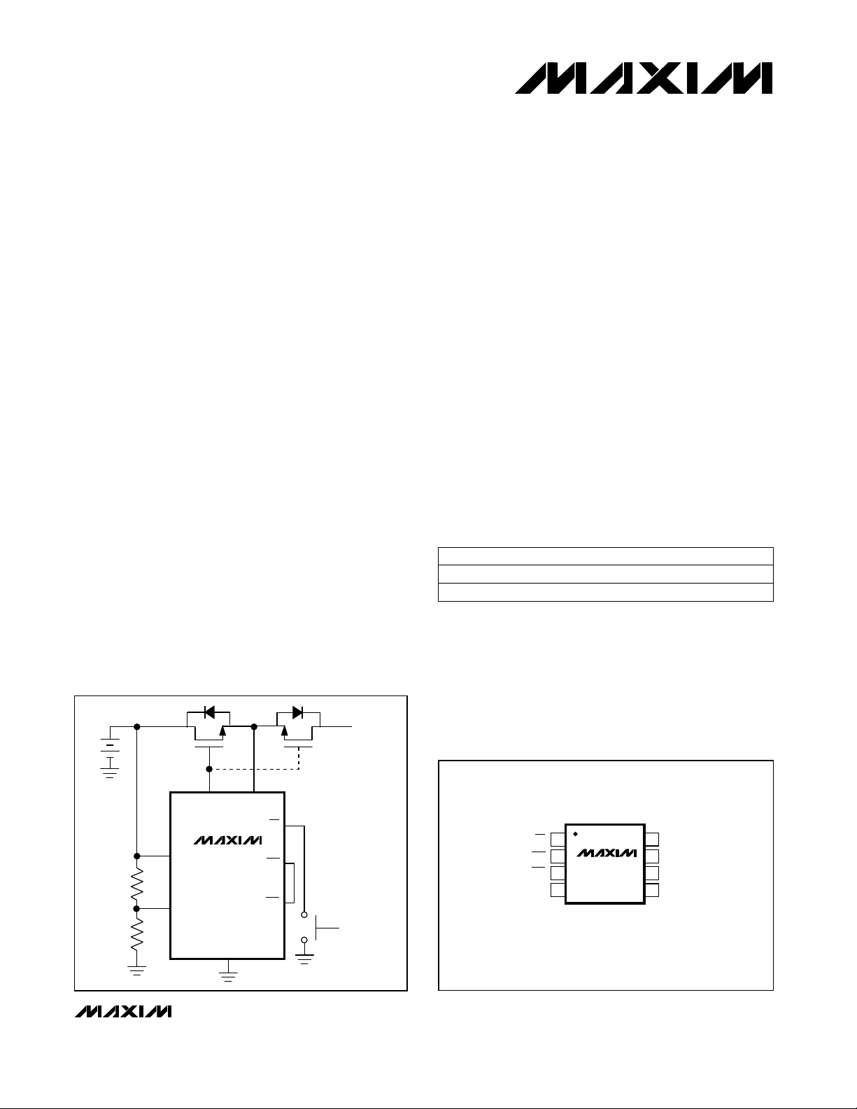
__________Typical Operating Circuit
NN
LOAD
__________________Pin Configuration
OPTIONAL FOR
REVERSE CURRENT
PROTECTION
SRCGATE
ON
MAX1614
BATT
R1
LBI
R2
GND
________________________________________________________________
OFF
LBO
TOP VIEW
ON
OFF
LBO
LBI
1
2
3
4
8
BATT
SRC
MAX1614
µMAX
Maxim Integrated Products
7
GATE
6
5
GND
1
For free samples & the latest literature: http://www.maxim-ic.com, or phone 1-800-998-8800
Page 2
High-Side, N-Channel MOSFET
OFF
Switch Driver
ABSOLUTE MAXIMUM RATINGS
BATT, SRC to GND.................................................-0.3V to +30V
GATE to SRC..........................................................-0.3V to +12V
GATE to GND.........................................................-0.3V to +36V
GATE + SRC Sink Current, Continuous.............................2.7mA
LBI, LBO, ON, OFF to GND....................................-0.3V to +12V
LBO Current..........................................................................5mA
Stresses beyond those listed under “Absolute Maximum Ratings” may cause permanent damage to the device. These are stress ratings only, and functional
operation of the device at these or any other conditions beyond those indicated in the operational sections of the specifications is not implied. Exposure to
MAX1614
absolute maximum rating conditions for extended periods may affect device reliability.
Continuous Power Dissipation (T
µMAX (derate 4.10mV/°C above +70°C) .....................330mW
Operating Temperature Range ...........................-40°C to +85°C
Junction Temperature......................................................+150°C
Storage Temperature Range.............................-65°C to +160°C
Lead Temperature (soldering, 10sec).............................+300°C
ELECTRICAL CHARACTERISTICS
(V
= 15V, TA= 0°C to +85°C, unless otherwise noted. Typical values are at TA= +25°C.)
BATT
CONDITIONS
V
- V
> 3V, SRC = BATT
SRC
= 26V, ON = OFF = unconnected,
= 1.5V
LBI
= 15V, ON = OFF = unconnected,
= 1.5V,
LBI
= 26V, ON = OFF = unconnected,
= 0A, device latched on, V
LBI
BATT
= 1.5V,
= 15V,
= 0A
= V
= V
SRC
BATT
= 15V
SRC
= 4V, device latched off
LBI
= V
BATT
/ 4
= 5V
= 26V
= 5V
= 5V,
BATT Shutdown Current
Quiescent Current
INTERNAL CHARGE PUMP
GATE Drive Voltage
LOW-BATTERY COMPARATOR
LBI Trip Level
LBI Trip Hysteresis
Minimum V
for Valid LBO
BATT
LBI Input Current
LBO Low Voltage
LBO High Leakage
CONTROL INPUTS (ON,
Input Low Voltage
Input High Voltage
Minimum Input Pulse Width
GATE
V
SHDN
I
BATT
I
SRC
BATT
I
GATE
V
BATT
I
GATE
SRC = BATT
+
V
I
GATE
= 0A, device latched off, V
= 0A, device latched on, V
BATT
SRC = BATT
Measured from GATE to SRC, V
I
V
GS
TH
GATE
Measured from GATE to SRC, V
I
= 1.5µA
GATE
V
GATE
V
GATE
LBI input falling
Tested at V
V
= 1.3V
LBI
OL
OH
LBI
I
SINK
V
LBO
= 1mA
= 11.5V
)
Tested at 2V
Tested at 0.6V
V
V
V
BATT
BATT
BATT
IL
IH
PW
= +70°C)
A
17 30
21 40
6.5 8 9.0
3
TH
UNITSMIN TYP MAXSYMBOLPARAMETER
V526BATT Operating Range
µA47I
µA
µA
V
µA15 60GATE Drive Output Current
mA0.5 2GATE Discharge Current
V1.182 1.20 1.218V
V0.02V
V0.9 4
nA10I
V0.4V
µA0.5V
µA0.5Minimum Input Pull-Up Current
µA1.5 2Maximum Input Pull-Up Current
V0.6V
V2.0V
µs0.5 1.0t
2 _______________________________________________________________________________________
Page 3
High-Side, N-Channel MOSFET
Switch Driver
ELECTRICAL CHARACTERISTICS
(V
= 15V, TA= -40°C to +85°C, unless otherwise noted.) (Note 1)
BATT
PARAMETER SYMBOL MIN TYP MAX UNITS
BATT Operating Range 5.0 26 V
BATT Shutdown Current
Quiescent Current
INTERNAL CHARGE PUMP
INTERNAL CHARGE PUMP
I
SHDN
I
BATT
I
SAC
V
- V
GATE
V
= 26V, ON = OFF = unconnected,
BATT
= 0A, device latched off, V
I
GATE
+
V
= 26V, ON = OFF = unconnected,
BATT
= 0A, device latched on, V
I
GATE
Measured from GATE to SRC, V
I
= 0A
GATE Drive Voltage V
GS
GATE Drive Output Current 15 60 µA
LOW BATTERY COMPARATOR
LOW-BATTERY COMPARATOR
LBI Trip Level V
TH
GATE
Measured from GATE to SRC, V
I
= 1.5µA, V
GATE
V
= V
GATE
LBI input falling
Note 1: Specifications to -40°C are guaranteed by design and not production tested.
CONDITIONS
> 3V, SRC = BATT
SRC
= 5.25V
SRC
= 15V
SRC
LBI
LBI
BATT
BATT
= 1.5V
= 1.5V
= 15V,
= 5.25V,
8 µA
40
6.5 9.0
3
1.176 1.20 1.224 V
MAX1614
µA
V
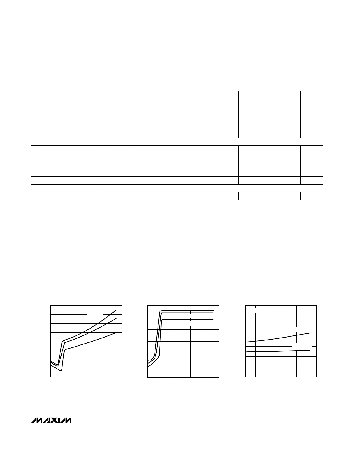
__________________________________________Typical Operating Characteristics
(TA = +25°C, unless otherwise noted.)
ON SUPPLY CURRENT
vs. V
V
BATT
BATT
TA = +85°C
20
(V)
= +25°C
T
A
T
= -40°C
A
25
MAX1614-01
4.0
3.5
3.0
2.5
2.0
SHUTDOWN CURRENT (µA)
1.5
1.0
530
10 15
22
20
18
16
14
12
SUPPLY CURRENT (µA)
10
8
6
530
10 15
_______________________________________________________________________________________ 3
OFF SUPPLY CURRENT
vs. V
BATT
TA = +85°C
TA = +25°C
= -40°C
T
A
20
V
(V)
BATT
1.30
MAX1614-02
1.28
1.26
1.24
1.22
LBI THRESHOLD (V)
1.20
1.18
25
1.16
LOW-BATTERY THRESHOLD
vs. TEMPERATURE
V
= 15V
BATT
V
RISING
LBI
V
FALLING
LBI
-40 100
-20 0
20 60
40
TEMPERATURE (°C)
80
MAX1614-05
Page 4

High-Side, N-Channel MOSFET
Switch Driver
____________________________Typical Operating Characteristics (continued)
(TA = +25°C, unless otherwise noted.)
GATE-DISCHARGE CURRENT
vs. GATE VOLTAGE
2.5
2.0
MAX1614
1.5
1.0
0.5
GATE-DISCHARGE CURRENT (mA)
0
-0.5
020
48
GATE AND SOURCE TRANSITIONS
FOR TYPICAL MOSFET LOAD
5V/div
34
T
= -40°C
A
= +25°C
T
A
TA = +85°C
12
16214610 18
V
(V)
GATE
MAX1614-04
33
32
31
30
29
28
GATE-CHARGING CURRENT (µA)
27
26
GATE-CHARGING CURRENT
vs. TEMPERATURE
V
= 15V
BATT
-40 0 80 100
40-20 6020
TEMPERATURE (°C)
MAX1614--03
GATE-CHARGING CURRENT
vs. BATT VOLTAGE
30
29
28
27
26
25
24
GATE-CHARGING CURRENT (µA)
23
22
530
10 15
V
BATT
(V)
T
A =
T
-40°C
A =
20
25
+85°C
MAX1614-06
GATE TURN-ON TRANSITION
FOR TYPICAL MOSFET LOAD
V
V
GATE
SRC
Si9936 MOSFETS
MAX1614-07
I
= 1A
LOAD
ON = GND
5V/div
0V
V
V
GATE
SRC
Si9936 MOSFETS
MAX1614-08
I
= 1A
LOAD
C
= 400pF
iss
ON = GND
V
V
OFF
1ms/div
OFF
0V
100µs/div
GATE TURN-OFF TRANSITION
FOR TYPICAL MOSFET LOAD
Si9936 MOSFETS
V
GATE
V
SRC
MAX1614-09
I
LOAD
C
iss
ON = GND
= 1A
= 400pF
5V/div
V
OFF
20µs/div
4 _______________________________________________________________________________________
Page 5

High-Side, N-Channel MOSFET
Switch Driver
______________________________________________________________Pin Description
PIN
1
2
3
ON
OFF
LBI4
GATE6
SRC7
SET Input to the On/Off Latch. Pulse ON low with OFF high to turn on the external MOSFET switch. When
both ON and OFF are low, the part is off.
RESET Input to the On/Off Latch. Pulse OFF low with ON high to turn off the external MOSFET switch. When
both ON and OFF are low, the part is off.
Open-Drain, Low-Battery Comparator Output. LBO is low when V
Low-Battery Comparator Input. LBO goes low when V
between BATT, LBI, and GND to set the battery undervoltage trip threshold (see
System GroundGND5
Gate-Drive Output. Connect to the gates of external, N-channel MOSFETs. When the MAX1614 is off, GATE
actively pulls to GND.
Source Input. Connect to the sources of external, N-channel MOSFETs. When the MAX1614 is off, SRC
actively pulls to GND.
Battery Input. Connect to a battery voltage between 5V and 26V.BATT8
_______________Detailed Description
The MAX1614 uses an internal, monolithic charge pump
and low-dropout linear regulator to supply the required
8V VGSvoltage to fully enhance an N-channel MOSFET
high-side switch (Figure 1). The charge pump typically
supplies 30µA, charging 800pF of gate capacitance in
400µs (V
add a small capacitor between the GATE and SRC
pins. When turned off, GATE and SRC pull low and typically discharge an 800pF gate capacitance in 80µs.
The MAX1614 provides separate on/off control inputs
(ON and OFF). ON and OFF connect, respectively, to
the SET and RESET inputs of an internal flip-flop. When
ON is pulsed low (with OFF = high), the internal charge
pump turns on, and GATE is pumped to 8V above SRC,
turning on the external MOSFETs. The charge pump
maintains gate drive to the external MOSFETs until OFF
is pulsed low. When this happens, the internal charge
pump turns off, and GATE discharges to ground
through an internal switch. For slower turn-on times,
simply add a small capacitor.
= 15V). For slower turn-on times, simply
BATT
__________ Applications Information
Connecting ON/
ON and OFF internally connect to 2µA max pull-up
current sources (Figure 1). The open-circuit voltage
for ON and OFF ranges from 7V to 10.5V (nominally
8.5V). Since the current sources are relatively weak,
connecting ON and OFF directly to logic powered from
OFF
to 3V or 5V Logic
FUNCTIONNAME
is below the trip point.LBO
LBI
falls below 1.20V (typ). Connect a voltage divider
LBI
lower voltages (e.g., 3V or 5V) poses no problem if the
gate outputs driving these pins can sink at least 2µA
while high.
Although the MAX1614 shutdown function was designed
to operate with a single pushbutton on/off switch, it can
also be driven by a single gate. Connect ON to GND
and drive OFF directly (Figure 2).
Typical Operating Circuit
).
Maximum Switching Rate
The MAX1614 is not intended for fast switching applications. In fact, it is specifically designed to limit the
rate of change of the load current, ∆I/∆t. The maximum
switching rate is limited by the turn-on time, which is a
function of the charge-pump output current and the
total capacitance on GATE (C
on time as a function of external MOSFET gate capacitance using the Gate Charging Current vs. V
in the
Typical Operating Characteristics
time is small compared to turn-on time, the maximum
switching rate is approximately 1/tON.
). Calculate the turn-
GATE
. Since turn-off
BATT
graph
Adding Gate Capacitance
The charge pump uses an internal monolithic transfer
capacitor to charge the external MOSFET gates.
Normally, the external MOSFET’s gate capacitance is
sufficient to serve as a reservoir capacitor. If the
MOSFETs are located at a significant distance from the
MAX1614, place a local bypass capacitor (100pF typ)
across the GATE and SRC pins. For slower turn-on
times, simply add a small capacitor between GATE and
SRC.
MAX1614
_______________________________________________________________________________________ 5
Page 6

High-Side, N-Channel MOSFET
Switch Driver
BATT
MAX1614
1.21V
LBI
LBO
P
8.5V
LDO
N
POWER-ON
RESET (BATT < 2V)
SOFT
START
1µA1µA
C
PUMP
P
N
50kHz
OSC
ON
GATE
SRC
OFF
ON
ON
OFF
STATE
0
0
OFF
0
1
1
0
1
1
GND
ON
OFF
LAST VALID
STATE
MAX1614
N
Figure 1. Functional Diagram
6 _______________________________________________________________________________________
Page 7

High-Side, N-Channel MOSFET
Switch Driver
SHUTDOWN
(CMOS OR TTL LOGIC)
Figure 2. Single-Line Shutdown Control
NN
MAX1614
OFF
GND
SRCGATE
ON
ON
LOAD
Simple Low-Battery Disconnect/Fresh
Battery Reconnect Circuit
A simple undervoltage disconnect circuit is often desirable to prevent damage to secondary batteries due to
repeated deep discharge or cell reversal. The
Operating Circuit
turns off the MAX1614, disconnecting
Typical
the battery from the load when the battery voltage
falls below the minimum battery voltage required,
(V
LOW BATT
). V
LOW BATT
= (R1 + R2) / R2 x VTHwhere
VTHis the LBI input threshold (1.20V typ). When fresh
cells are installed or the batteries are recharged, a µC
or pushbutton reconnects the load.
Using
LBO
to Generate Early
Power-Fail Interrupt
Many applications require an early warning indicating
that power is failing so that the microprocessor (µP)
can take care of any “housekeeping” functions (storing
current settings in memory, etc.) before the power fails.
Connect LBI through a resistor divider across the battery, and connect LBO to the µP nonmaskable interrupt
(NMI). Set the threshold so that LBO goes low when the
battery decays to a point where regulation begins to
degrade (Figure 4). V
LOW BATT
where VTHis the LBI input threshold (1.20V typ). Once
housekeeping is complete, the µP can turn off the load
by pulling OFF low.
= (R1 + R2) / R2 x V
TH,
MAX1614
MAX1614
BATT
R1
LBI
R2
GND
Figure 3. Single-Pushbutton On/Off Control
OFF
LBO
TO µC
On/Off Control with a
Single Pushbutton Switch
The MAX1614’s separate on and off inputs allow maximum flexibility in controlling the external MOSFETs.
Connect a pushbutton switch to the ON pin and microcontroller (µC) I/O for single-button control. Connect the
OFF pin to another µC I/O pin. On the first button
depression, the MAX1614 turns on automatically; the
signal is also detected by the µC. When the button is
depressed a second time, the µC wraps around and
turns off the MAX1614 by pulling low on the OFF pin
(Figure 3).
_______________________________________________________________________________________ 7
NN
SRCGATE
ON
MAX1614
BATT
R1
LBI
R2
GND
Figure 4. Using LBO to Generate Early Power-Fail Interrupt
OFF
LBO
LOAD
TO µC
PORT PINS
TO µC
NONMASKABLE
INTERRUPT
Page 8

High-Side, N-Channel MOSFET
Switch Driver
Increasing Low-Battery
Comparator Hysteresis
The MAX1614 contains an on-chip comparator with 2%
hysteresis for low-battery detection. If more than 2%
hysteresis is needed on the low-battery comparator and
LBO is connected to OFF, use the circuit in Figure 5 to
add hysteresis. The circuit of Figure 5 shows LBO con-
trolling an N-channel MOSFET that shorts R2 to add
positive feedback to the trip point. This is necessary to
MAX1614
prevent loading down the 1µA pull-up at OFF (Figure 1).
2N7002
(SOT23)
___________________Chip Information
TRANSISTOR COUNT: 264
SUBSTRATE CONNECTED TO GND
R1 = 909kΩ
R2, R3 = 150kΩ
= 8.5V
V
L
= 9.8V
V
H
HYSTERESIS = 6%
Figure 5. Increasing Hysteresis of the Battery Disconnect
Circuit
BATT
R1
R2N
LBI
R3
FALLING TRIP POINT V
= VTH
V
L
N
SRCGATE
MAX1614
GND
R1 + R3
( )
R3
OFF
LBO
L
ON
RISING TRIP POINT VH
= VTH
V
H
LOAD
R1 + R2 + R3
( )
R3
________________________________________________________________Package Information
DIM
C
A
0.101mm
e
A1B
E H
0.004 in
L
α
A1
C
D
H
8-PIN µMAX
MICROMAX SMALL-OUTLINE
PACKAGE
D
Maxim cannot assume responsibility for use of any circuitry other than circuitry entirely embodied in a Maxim product. No circuit patent licenses are
Maxim cannot assume responsibility for use of any circuitry other than circuitry entirely embodied in a Maxim product. No circuit patent licenses are
Maxim cannot assume responsibility for use of any circuitry other than circuitry entirely embodied in a Maxim product. No circuit patent licenses are
implied. Maxim reserves the right to change the circuitry and specifications without notice at any time.
implied. Maxim reserves the right to change the circuitry and specifications without notice at any time.
implied. Maxim reserves the right to change the circuitry and specifications without notice at any time.
8
___________________Maxim Integrated Products, 120 San Gabriel Drive, Sunnyvale, CA 94086 (408) 737-7600
8
___________________Maxim Integrated Products, 120 San Gabriel Drive, Sunnyvale, CA 94086 (408) 737-7600
8
___________________Maxim Integrated Products, 120 San Gabriel Drive, Sunnyvale, CA 94086 (408) 737-7600
© 1996 Maxim Integrated Products Printed USA is a registered trademark of Maxim Integrated Products.
© 1996 Maxim Integrated Products Printed USA is a registered trademark of Maxim Integrated Products.
© 1996 Maxim Integrated Products Printed USA is a registered trademark of Maxim Integrated Products.
INCHES MILLIMETERS
A
0.036
0.004
B
0.010
0.005
0.116
E
0.116
e
0.188
L
0.016
α
MIN
0°
MAX
0.044
0.008
0.014
0.007
0.120
0.120
0.198
0.026
6°
MIN
0.91
0.10
0.25
0.13
2.95
2.95
4.78
0.41
0°
MAX
1.11
0.20
0.36
0.18
3.05
3.05
0.650.0256
5.03
0.66
6°
21-0036D
 Loading...