

Page 1
MAX1600/MAX1603
Dual-Channel CardBus and PCMCIA VCC/VPP
Power-Switching Networks
________________________________________________________________
Maxim Integrated Products
1
For free samples & the latest literature: http://www.maxim-ic.com, or phone 1-800-998-8800.
For small orders, phone 408-737-7600 ext. 3468.
19-4752; Rev 3; 5/98
PART
MAX1600EAI
MAX1603EAI
-40°C to +85°C
-40°C to +85°C
TEMP. RANGE PIN-PACKAGE
28 SSOP
28 SSOP
General Description
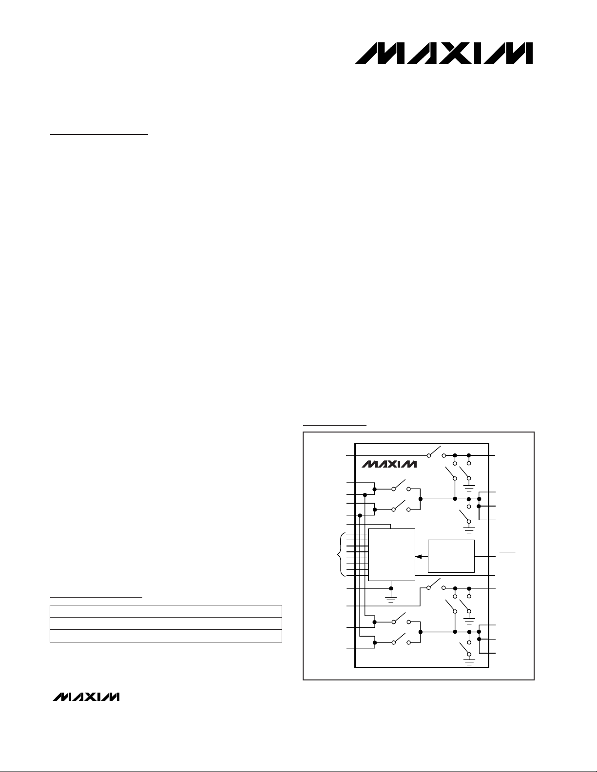
The MAX1600/MAX1603 DC power-switching ICs contain a network of low-resistance MOSFET switches that
deliver selectable VCC and VPP voltages to two
CardBus or PC Card host sockets. Key features include
ultra-low-resistance switches, small packaging, softswitching action, and compliance with PCMCIA specifications for 3V/5V switching. 3.3V-only power switching
for fast, 32-bit CardBus applications is supported in two
ways: stiff, low-resistance 3.3V switches allow high 3.3V
load currents (up to 1A); and completely independent
internal charge pumps let the 3.3V switch operate normally, even if the +5V and +12V supplies are disconnected or turned off to conserve power. The internal
charge pumps are regulating types that draw reduced
input current when the VCC switches are static. Also,
power consumption is automatically reduced to 10µA
max when the control logic inputs are programmed to
high-Z or GND states, unlike other solutions that may
require a separate shutdown-control input.
Other key features include guaranteed specifications
for output current limit level, and guaranteed specifications for output rise/fall times (in compliance with
PCMCIA specifications). Reliability is enhanced by
thermal-overload protection, accurate current limiting,
an overcurrent-fault flag output, and undervoltage lockout. The CMOS/TTL-logic interface is flexible, and can
tolerate logic input levels in excess of the positive supply rail.
The MAX1600 and MAX1603 are identical, except for
the MAX1603’s VY switch on-resistance (typically
140mΩ). The MAX1600/MAX1603 fit two complete
CardBus/ PCMCIA switches into a space-saving, narrow
(0.2in. or 5mm wide) SSOP package.
________________________Applications
Desktop Computers Data Loggers
Notebook Computers Docking Stations
Handy-Terminals PCMCIA Read/Write Drives
Ordering Information
____________________________Features
♦ Supports Two PC Card/CardBus Sockets
♦ 1A, 0.08Ω Max 3.3V VCC Switch (MAX1600 only)
1A, 0.14Ω Max 5V VCC Switch
♦ Soft Switching for Low Inrush Surge Current
♦ Overcurrent Protection
♦ Overcurrent/Thermal-Fault Flag Output
♦ Thermal Shutdown at Tj= +150°C
♦ Independent Internal Charge Pumps
♦ Break-Before-Make Switching Action
♦ 10µA Max Standby Supply Current
♦ 5V and 12V Not Required for Low-R
DS(ON)
3.3V Switching
♦ Complies with PCMCIA 3V/5V Switching
Specifications
♦ Super-Small 28-Pin SSOP Package
(0.2in. or 5mm wide)
♦ Code Compatible with:
Cirrus CL-PD67XX Family
Databook DB86184
Intel 82365SL (industry-standard coding)
DECODE
LOGIC
VY
12IN
VY
VX
VX
OVERCURRENT
AND
THERMAL
SHUTDOWN
MAX1600/MAX1603
VDD
CODE
SELECT
GND
12IN
VY
VX
VL
VPPA
VCCA
VCCA
VCCA
FAULT
CODE
VPPB
VCCB
VCCB
VCCB
CONTROL
INPUTS
Simplified Block Diagram
Pin Configuration appears on last page.
Page 2
MAX1600/MAX1603
Dual-Channel CardBus and PCMCIA VCC/VPP
Power-Switching Networks
2 _______________________________________________________________________________________
ABSOLUTE MAXIMUM RATINGS
ELECTRICAL CHARACTERISTICS
(VL = VY = 3.3V, VX = 5V, 12INA = 12INB = 12V, TA= 0°C to +85°C, unless otherwise noted. Typical values are at TA= +25°C.)
Stresses beyond those listed under “Absolute Maximum Ratings” may cause permanent damage to the device. These are stress ratings only, and functional
operation of the device at these or any other conditions beyond those indicated in the operational sections of the specifications is not implied. Exposure to
absolute maximum rating conditions for extended periods may affect device reliability.
Inputs/Outputs to GND
(VL, VX, VY, VCCA, VCCB) (Note 1)........................-0.3V, +6V
VPP Inputs/Outputs to GND
(12INA, 12INB, VPPA, VPPB) (Note 1)..................-0.3V, +15V
Logic Inputs to GND (A0VCC, A1VCC, B0VCC, B1VCC,
A0VPP, A1VPP, B0VPP, B1VPP) (Note 1) ...............-0.3V, +6V
CODE Input to GND.........................................-0.3V, (VL + 0.3V)
VCCA, VCCB Output Current (Note 2).....................................4A
VPPA, VPPB Output Current (Note 2)...............................250mA
VCCA, VCCB Short Circuit to GND............................Continuous
VPPA, VPPB Short Circuit to GND..............................Continuous
Continuous Power Dissipation (T
A
= +70°C)
SSOP (derate 9.52mW/°C above +70°C) ....................762mW
Operating Temperature Range
MAX160_EAI/MAX1603EAI..............................-40°C to +85°C
Storage Temperature Range.............................-65°C to +160°C
Lead Temperature (soldering, 10sec).............................+300°C
2.4 2.5 2.8
V
11 13
Input Voltage Range
µA25 150VL Quiescent Supply Current
µA1Standby Supply Current
µA15 10012IN_ Quiescent Supply Current
µA4 10VL Standby Supply Current
UNITSMIN TYP MAXPARAMETER
VX or VY, all switches 0V or high-Z,
control inputs = 0V or VL, TA= +25°C
1 µA12IN_ Standby Supply Current
3.0 5.5
Ω
0.06 0.08
A0 1Operating Output Current Range
Ω0.10 0.14On-Resistance, VX Switches
µA20 100VY Quiescent Supply Current
µA20 100VX Quiescent Supply Current
V/µs0.05VL Fall Rate
1.8 3.0
V
1.4 2.5 2.8
Undervoltage Lockout Threshold
5.0 8.0 10.0
VL falling edge
When using VL as shutdown pin (Note 3)
VX, VY or VL
12INA, 12INB
Any combination of VY switches on,
control inputs = 0V or VL, no VCC loads
MAX1600
VCCA or VCCB, VX = VY = 3V to 5.5V
Any combination of switches on
12INA tied to 12INB, VPPA and VPPB 12V switches on,
control inputs = 0V or VL, no VPP loads
CONDITIONS
12IN falling edge
12INA tied to 12INB, all switches 0V or high-Z,
control inputs = 0V or VL, TA= +25°C
12INA = 12INB = 0V to 13V, VX = 4.5V, VY = 0V to 5.5V,
I
SWITCH
= 1A, TA= +25°C
Any combination of VX switches on,
control inputs = 0V or high-Z, no VCC loads
12IN rising edge
VX, VY falling edge
12INA = 12INB = 0V to 13V,
VY = 3V, VX = 0V to 5.5V,
I
SWITCH
= 1A, TA= +25°C
0.14 0.24
On-Resistance, VY Switches
MAX1603
All switches 0V or high-Z,
control inputs = 0V or VL, TA= +25°C
A1.2 4Output Current Limit VCCA or VCCB
POWER-SUPPLY SECTION
VCC SWITCHES
Note 1: There are no parasitic diodes between any of these pins, so there are no power-up sequencing restrictions (for example,
logic input signals can be applied even if all of the supply voltage inputs are grounded).
Note 2: VCC and VPP outputs are internally current limited. See the
Electrical Characteristics
.
Page 3
MAX1600/MAX1603
Dual-Channel CardBus and PCMCIA VCC/VPP
Power-Switching Networks
_______________________________________________________________________________________ 3
ELECTRICAL CHARACTERISTICS (continued)
(VL = VY = 3.3V, VX = 5V, 12INA = 12INB = 12V, TA= 0°C to +85°C, unless otherwise noted. Typical values are at TA= +25°C.)
VCCA or VCCB, 0V to VX or VY, CL= 30µF,
RL= 25Ω, 50% of input to 90% of output, TA= +25°C
Hysteresis = 20°C (Note 4)
V
FAULT
= 5.5V, high state
I
SINK
= 1mA, low state
VPPA or VPPB forced to 0V, high-Z state, TA= +25°C
VCC_ or VPP_, load step to FAULT output,
50% point to 50% point (Note 3)
VPPA or VPPB < 0.4V, programmed to 0V state
VPPA or VPPB, programmed to 12V
VPPA or VPPB
12IN = 11.6V, I
SWITCH
= 100mA, TA= +25°C
Programmed to VX (5V) or VY (3.3V), TA= +25°C
VPPA or VPPB, 0V to 12IN_, CL= 0.1µF,
50% of input to 90% of output, T
A
= +25°C
CONDITIONS
°C150Thermal Shutdown Threshold
µA-0.5 0.5
FAULT Output Leakage Current
V0.4
FAULT Output Low Voltage
µs1
FAULT Signal Propagation Delay
ms1.2 30
Output Propagation Delay
Plus Rise Time
ms2 10
Output Propagation Delay
Plus Rise Time
µA10Output Leakage Current
mA10Output Sink Current
mA130 200 260Output Current Limit
mA0 120Operating Output Current Range
Ω0.70 1On-Resistance, 12V Switches
Ω1 3On-Resistance, VPP = VCC Switches
UNITSMIN TYP MAXPARAMETER
VCCA or VCCB, VX or VY to 0V, CL= 30µF,
RL= open circuit, 50% of input to 10% of output,
TA= +25°C
ms60 100
Output Propagation Delay
Plus Fall Time
VCCA or VCCB, VX or VY to 0V, CL= 1µF,
RL= 25Ω, 90% to 10% points
ms6Output Fall Time
“Databook” code
“Cirrus” code
“Intel” code
__VCC, __VPP
__VCC, __VPP
V1.2 VL - 1.2Code Input Mid-Level Voltage
VVL - 0.4 VLCode Input High Voltage
V0 0.4Code Input Low Voltage
V1.5Logic Input High Voltage
V0.6Logic Input Low Voltage
VPPA or VPPB, 0V to 12IN_, CL= 0.1µF,
10% to 90% points, TA= +25°C
µs100 800Output Rise Time
__VCC, __VPP, code µA-1 1Logic Input Bias Current
VCCA or VCCB, 0V to VX or VY, CL= 1µF,
RL= open circuit, 10% to 90% points, TA= +25°C
µs100 1200Output Rise Time
VPPA or VPPB, 12IN_ to 0V, CL= 0.1µF,
90% to 10% points
VPPA or VPPB, 12IN_ to 0V, CL= 0.1µF,
50% of input to 10% of output, TA= +25°C
ms1Output Fall Time
ms9 60
Output Propagation Delay
Plus Fall Time
VCCA or VCCB forced to 0V, high-Z state, TA= +25°C µA10Output Leakage Current
VCCA or VCCB < 0.4V, programmed to 0V state mA20Output Sink Current
VPP SWITCHES
INTERFACE AND LOGIC SECTION
Page 4
MAX1600/MAX1603
Dual-Channel CardBus and PCMCIA VCC/VPP
Power-Switching Networks
4 _______________________________________________________________________________________
ELECTRICAL CHARACTERISTICS
(VL = VY = 3.3V, VX = 5V, 12INA = 12INB = 12V, TA= -40°C to +85°C, unless otherwise noted.)
VX or VY, all switches 0V or high-Z,
control inputs = 0V or VL, TA= T
MIN
to T
MAX
12INA tied to 12INB, all switches 0V or high-Z,
control inputs = 0V or VL
All switches 0V or high-Z, control inputs = 0V or VL
V
3.0 5.5
0.6
µA100VY Quiescent Supply Current
VL falling edge, hysteresis = 1%
Logic Input Low Voltage __VCC, __VPP
VX, VY or VL
15
12INA, 12INB
µA12IN_ Standby Supply Current
1.8
µA100
Any combination of VY switches on,
control inputs = 0V or VL, no VCC loads
VX Quiescent Supply Current
V
1.4 2.9
Undervoltage Lockout Threshold
5 10
Any combination of switches on
12INA tied to 12INB, VPPA and VPB 12V switches on,
control inputs = 0V or VL, no VPP loads
CONDITIONS
12IN falling edge
2.3 2.9
V
11 13
Any combination of VX switches on,
control inputs = 0V or high-Z, no VCC loads
12IN rising edge
Input Voltage Range
VX, VY falling edge
µA150VL Quiescent Supply Current
µA15Standby Supply Current
µA10012IN_ Quiescent Supply Current
µA15VL Standby Supply Current
UNITSMIN TYP MAXPARAMETER
V1.6Logic Input High Voltage __VCC, __VPP
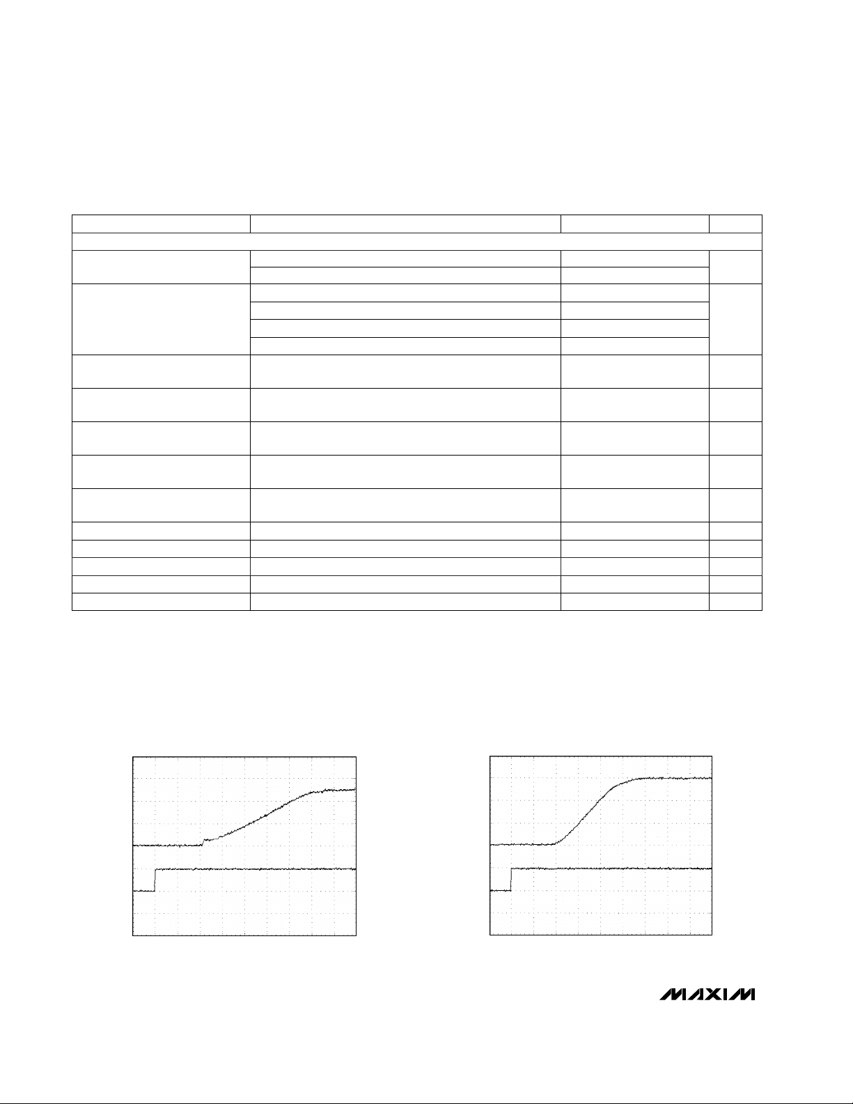
__________________________________________Typical Operating Characteristics
(VL = VY = 3.3V, VX = 5V = 12IN, TA = +25°C, unless otherwise noted.)
CL = 30µF, RL = 25Ω
VCC_ SWITCHING (RISE)
6
4
2
0
5
0
200µs/div
VCC_
(V)
CONTROL
INPUT
(V)
MAX1600/3 TOC-01
CL = 1µF, RL = ∞
VCC_ SWITCHING (RISE)
3
2
1
0
5
0
500µs/div
VCC_
(V)
CONTROL
INPUT
(V)
MAX1600/3 TOC-02
V0.4
FAULT Output Low Voltage
I
SINK
= 1mA, low state
POWER-SUPPLY SECTION
Note 3: Not production tested.
Note 4: Thermal limit not active in standby state (all switches programmed to GND or high-Z state).
Page 5

MAX1600/MAX1603
Dual-Channel CardBus and PCMCIA VCC/VPP
Power-Switching Networks
_______________________________________________________________________________________
5
_____________________________Typical Operating Characteristics (continued)
(VL = VY = 3.3V, VX = 5V = 12IN, TA = +25°C, unless otherwise noted.)
CL = 33µF, RL = ∞
VCC_ SWITCHING (FALL)
6
4
2
0
5
0
10ms/div
VCC_
(V)
CONTROL
INPUT
(V)
MAX1600/3 TOC-03
CL = 0.1µF, RL = ∞
VPP_ SWITCHING (RISE)
15
10
5
0
5
0
200µs/div
VPP_
(V)
CONTROL
INPUT
(V)
MAX1600/3 TOC-05
CL = 1µF, RL = 25
Ω
VCC_ SWITCHING (FALL)
6
4
2
0
5
0
10ms/div
VCC_
(V)
CONTROL
INPUT
(V)
MAX1600/3 TOC-04
VPP_ SWITCHING (FALL)
15
10
5
0
5
0
2ms/div
VPP_
(V)
CONTROL
INPUT
(V)
MAX1600/3 TOC-06
CL = 0.1µF, RL = ∞
CL = 1µF, RESISTIVE OVERLOAD, RL = 1Ω
VCC_ CURRENT LIMITING
4
2
0
2ms/div
VCC_
(V)
MAX1600/3 TOC-08
INPUT CURRENT (VCC OUTPUT SHORTED)
1.5
2.0
1.0
0.5
0
1ms/div
I
VY
(A)
MAX1600/3 TOC-09
Page 6

MAX1600/MAX1603
Dual-Channel CardBus and PCMCIA VCC/VPP
Power-Switching Networks
6 _______________________________________________________________________________________
_____________________________Typical Operating Characteristics (continued)
(VL = VY = 3.3V, VX = 5V = 12IN, TA = +25°C, unless otherwise noted.)
0
0 10 12
12IN SUPPLY CURRENT
vs. INPUT VOLTAGE
3
MAX1600/3 TOC-18
INPUT VOLTAGE (V)
12IN SUPPLY CURRENT (µA)
2 4 6 8
7
5
1
2
4
6
0
0 5 6
VL SUPPLY CURRENT
vs. VL INPUT VOLTAGE
30
MAX1600/3 TOC-19
INPUT VOLTAGE (V)
VL SUPPLY CURRENT (µA)
1 2 3 4
70
50
10
20
40
60
VX = VY = 0V
12IN
NORMAL
OPERATION
SHUTDOWN
CL = 1µF, RL = 50Ω
VPP_ CURRENT LIMITING
10
5
0
2ms/div
VPP_
(V)
MAX1600/3 TOC-10
RL = 0.1Ω
INPUT CURRENT (VPP OUTPUT SHORTED)
10
5
0
200
300
100
0
100µs/div
VPP_
(V)
I
12IN_
(mA)
MAX1600/3 TOC-11
CIRCUIT OF FIGURE 2
VCC_ SHUTDOWN RESPONSE
4
2
0
4
2
0
100µs/div
VL
(V)
VCC_
(V)
MAX1600/3 TOC-12
Page 7

MAX1600/MAX1603
Dual-Channel CardBus and PCMCIA VCC/VPP
Power-Switching Networks
_______________________________________________________________________________________
7
_____________________________Typical Operating Characteristics (continued)
(VL = VY = 3.3V, VX = 5V = 12IN, TA = +25°C, unless otherwise noted.)
80
30
0 1000
MAX1600
VY ON-RESISTANCE vs. CURRENT
40
70
MAX1600/3 TOC-14
CURRENT (mA)
VY R
ON
(mΩ)
200 400 600 800
60
50
35
45
75
65
55
TA = +85°C
TA = +25°C
TA = -40°C
165
115
0 1000
MAX1603
VY ON-RESISTANCE vs. CURRENT
125
155
MAX1600/3 TOC-20
CURRENT (mA)
VY R
ON
(mΩ)
200 400 600 800
145
135
120
130
160
150
140
TA = +85°C
TA = +25°C
TA = -40°C
685
0 100 120 140
12IN_ ON-RESISTANCE vs. CURRENT
700
MAX1600/3 TOC-15
CURRENT (mA)
12IN R
ON
(mΩ)
20 40 60 80
720
710
690
695
705
725
715
VPPA
VPPB
550
-40 60 80 100
12IN_ ON-RESISTANCE vs. TEMPERATURE
700
MAX1600/3 TOC-16
TEMPERATURE (°C)
12IN R
ON
(mΩ)
-20 0 20 40
900
800
600
650
750
950
850
0
0 5 6
VX, VY SUPPLY CURRENT
vs. INPUT VOLTAGE
0.3
MAX1600/3 TOC-17
INPUT VOLTAGE (V)
VX, VY SUPPLY CURRENT (µA)
1 2 3 4
0.7
0.5
0.1
0.2
0.4
0.8
0.9
0.6
VX
VY
Channel A VPP Control Input. See
Logic Truth Tables
.A1VPP2
Channel B VCC OutputsVCCB9, 18, 20
Channel B VPP OutputVPPB11
+12V Supply Voltage Input, internally connects to channel B VPP switch. Tie to VPPB if not used.12INB12
Channel A VPP OutputVPPA5
Channel A VCC OutputsVCCA7, 22, 24
+12V Supply Voltage Input, internally connects to channel A VPP switch. Tie to VPPA if not used.12INA4
PIN
GroundGND1
NAME FUNCTION
Channel A VPP Control Input. See
Logic Truth Tables
.A0VPP3
Pin Description
110
60
0 1000
VX ON-RESISTANCE
vs. VCC_ LOAD CURRENT
70
100
MAX1600/3 TOC-13
VCC_ LOAD CURRENT (mA)
VX R
ON
(mΩ)
200
400 600 800
90
80
65
75
105
95
85
TA = +85°C
TA = +25°C
TA = -40°C
VX Supply Voltage Inputs. VX pins must be connected to one another. Input range is +3V to
+5.5V. VX is normally connected to 5V.
VX6, 8, 10
Page 8

MAX1600/MAX1603
Dual-Channel CardBus and PCMCIA VCC/VPP
Power-Switching Networks
8 _______________________________________________________________________________________
Table 1. Standard “Intel” Code (82365SL),
CODE = GND
Table 2. “Cirrus” Code,
CODE = High (VL)
STBY = Standby Mode STBY = Standby Mode
MODE
ACTIVE
ACTIVE
ACTIVE
STBY
ACTIVE
ACTIVE
ACTIVE
ACTIVE
STBY
STBY
STBY
ACTIVE
ACTIVE
ACTIVE
ACTIVE
ACTIVE
_0VPP VPP_
0 12IN
1 VCC_
0 GND
1 GND
1 High-Z
0 GND
1 VCC_
0 12IN
1
0 GND
GND
0 GND
1 High-Z
0 GND
1 VCC_
0 12IN
1 High-Z
VCC_
VX
VY
VY
VY
VY
GND
VY
VX
VY
VY
VX
VX
VY
GND
GND
GND
_1VCC _1VPP
0 1
0 0
0 0
0 1
0 1
1 0
1 0
1 1
0
0 0
0
0 1
1 1
1 0
1 0
1 1
1 1
_0VCC
0
1
1
1
1
0
1
0
1
1
0
0
1
0
0
0
Pin Description (continued)
Channel B VCC Control Input. See
Logic Truth Tables.
B1VCC16
Channel B VPP Control Input. See
Logic Truth Tables.
B1VPP14
Channel A VCC Control Input. See
Logic Truth Tables.
A1VCC26
Three-Level Code-Select Input. See
Logic Truth Tables
.
Low = Standard “Intel” code
High = “Cirrus” code
Mid-supply = “Databook” code (Figure 6)
CODE25
Logic Supply-Voltage Input. Connect to the +3.3V or +5V host system supply. VL can be supplied
via the output of a CMOS-logic gate to produce an overriding shutdown. When used as a
shutdown input, VL should have a 1kΩ series resistor with a 0.1µF capacitor to ground (Figure 2).
Note that VL must be greater than undervoltage lockout for any switches to be turned on.
VL28
VY Supply Voltage Inputs. VY pins must be connected to one another. Input range is +3V to +5.5V.
VY is normally connected to 3.3V.
VY19, 21, 23
Fault-Detection Output. FAULT goes low during current limit, undervoltage lockout, or thermal
limit. FAULT is an open-drain output that requires an external pull-up resistor.
FAULT
17
Channel B VCC Control Input. See
Logic Truth Tables.
B0VCC15
Channel B VPP Control Input. See
Logic Truth Tables.
B0VPP13
PIN NAME FUNCTION
Channel A VCC Control Input. See
Logic Truth Tables.
A0VCC27
Logic Truth Tables
MODE
ACTIVE
ACTIVE
ACTIVE
STBY
ACTIVE
ACTIVE
ACTIVE
_1VCC
ACTIVE
STBY
_1VPP
0
STBY
STBY
1
0
ACTIVE
STBY
0
0
STBY
STBY
0
0
STBY
1
0
_0VPP
1
1
VPP_
0
0
1
12IN
1
0
1
VCC_
0
1
0
0
GND
1
0
High-Z
1
0
0
High-Z
0
1
1
GND
1
1
1
VCC_
0
0
1
12IN
1
0
1
0 High-Z
1
1
High-Z
0
1
High-Z
1 High-Z
0 GND
1 GND
0 GND
1 GND
VCC_
VY
VX
GND
VX
VX
High-Z
VX
VY
GND
GND
VY
VY
_0VCC
0
1
1
1
1
0
1
0
1
1
0
0
1
0
GND
0
0
High-Z
High-Z
High-Z
Page 9

MAX1600/MAX1603
Dual-Channel CardBus and PCMCIA VCC/VPP
Power-Switching Networks
_______________________________________________________________________________________ 9
Logic Truth Tables (cont.)
Table 3. “Databook” Code,
CODE = Mid-Supply (VL/2)
STBY = Standby Mode X = Don’t Care
MODE
ACTIVE
ACTIVE
ACTIVE
ACTIVE
ACTIVE
_1VCC
STBY
_1VPP
1
ACTIVE
STBY
0
1 1
1 0
0 1
1
_0VPP
1
VPP_
X VCC_
X GND
X
0
0
VCC_
X
0
12IN
X
1
0
GND
0
X
X High-Z
12IN
X GND
VCC_
VX
VY
VY
VX
VX
_0VCC
1
0
0
1
1
0
0
1
GND
VY
GND
Figure 1. Detailed Block Diagram (one channel of two)
Detailed Description
The MAX1600/MAX1603 power-switching ICs contain a
network of low-resistance MOSFET switches that deliver
selectable VCC and VPP voltages to two CardBus or
PC Card host sockets. The MAX1600/MAX1603 differ
only in the VY switch on-resistance. Figure 1 is the
detailed block diagram.
The power-input pins (VY, VX, 12IN_) are completely
independent. Low inrush current is guaranteed by controlled switch rise times. VCC’s 100µs minimum output
rise time is 100% tested with a 1µF capacitive load, and
VPP’s 1ms minimum rise time is guaranteed with a 0.1µF
load. These respective capacitive loads are chosen as
worst-case card-insertion parameters. The internal
switching control allows VCC and VPP rise times to be
1/2 MAX1600
1/2 MAX1603
VY
VB12
CHARGE
PUMP
VB3
0.08Ω*
CURRENT
LIMIT
VPPA12IN
3Ω
40Ω
VY
CHARGE
PUMP
VX
VX
CONTROL
INPUTS
VB5
CHARGE
PUMP
DECODE
LOGIC
AND UVLO
VDD
VL
0.14Ω
SHDN
CURRENT
LIMIT
CURRENT
LIMIT
THERMAL
SHUTDOWN
VCCA
VCCA
VCCA
20Ω
FAULT
GND
* 0.24Ω FOR THE MAX1603
Page 10

MAX1600/MAX1603
Dual-Channel CardBus and PCMCIA VCC/VPP
Power-Switching Networks
10 ______________________________________________________________________________________
controlled, and makes them nearly independent of resistive and capacitive loads (see rise-time photos in the
Typical Operating Characteristics
). Fall times are a
function of loading, and are compensated by internal
circuitry.
Power savings is automatic: internal charge pumps draw
very low current when the VCC switches are static.
Standby mode reduces switch supply current to 1µA.
Driving the VL pin low with an external logic gate (master
shutdown) reduces total supply current to1µA (Figure 2).
Operating Modes
The MAX1600/MAX1603 are compatible with the Cirrus
CL-PD67XX, Databook DB86184, and Intel 82365SL PC
Card Interface Controllers (PCIC). Eight control inputs
select the internal switches’ positions and the operating
modes according to the input code. Select the proper
code format for the chosen controller with the CODE
input pin (see
Pin Description
and Tables 1, 2, and 3).
CODE reconfigures the logic decoder to one of three
interface controllers:
Low = Standard “Intel” code (Figure 5)
High = “Cirrus” code (Figure 4)
Midsupply = “Databook” code (Figure 6)
An additional 1µA (3µA max) of VL supply current will
flow if CODE = midsupply (VL / 2).
The MAX1600/MAX1603 have three operating modes:
normal, standby, and shutdown. Normal mode supplies
the selected outputs with their appropriate supply voltages. Standby mode places all switches at ground,
high impedance, or a combination of the two. Shutdown
mode turns all switches off, and puts the VCC and VPP
outputs into a high-impedance state. Pull VL low to
enter shutdown mode. To ensure a 0.05V/µs fall rate on
VL, use a 1kΩ series resistor and a 0.1µF capacitor to
ground (Figure 2).
Overcurrent Protection
Peak detecting circuitry protects both the VCC and VPP
switches against overcurrent conditions. When current
through any switch exceeds the internal current limit
(4A for VCC switches and 200mA for VPP switches) the
switch turns off briefly, then turns on again at the controlled rise rate. If the overcurrent condition lasts more
than 2µs, the FAULT output goes low. FAULT is not
latched. A continuous short-circuit condition results in a
pulsed output current and a pulsed FAULT output until
thermal shutdown is reached. FAULT is open-drain and
requires an external pull-up resistor.
Thermal Shutdown
If the IC junction temperature rises above +150°C, the
thermal shutdown circuitry opens all switches, including
the GND switches, and FAULT is pulled low. When the
temperature falls below +130°C, the switches turn on
again at the controlled rise rate. If the overcurrent condition remains, the part cycles between thermal shutdown and overcurrent.
Undervoltage Lockout
If the VX or VY switch input voltage drops below 1.5V,
the associated switch turns off and FAULT goes low.
For example, if VY is 3.3V and VX is 0V, and if the interface controller selects VY, the VCCA output will be
3.3V. If VX is selected, VCCA changes to a high-impedance output and FAULT goes low.
When a voltage is initially applied to 12IN_, it must be
greater than 8V to allow the switch to operate.
Operation continues until the voltage falls below 2V (the
VPP output is high impedance).
When VL drops to less than 2.3V, all switches are
turned off and the VCC and VPP outputs are high
impedance.
MAX1600
MAX1603
1k
0.1µF
74HC04
VL
VY
VCCA
VPPA
3.3V
VPPB
VCCB
TO
SOCKETS
A AND B
Figure 2. Master Shutdown Circuit
MAX1600
MAX1603
VL
VX+5V
VY
Figure 3. Applying Power to the VL Input
Page 11

MAX1600/MAX1603
Dual-Channel CardBus and PCMCIA VCC/VPP
Power-Switching Networks
______________________________________________________________________________________ 11
A0VCC
A1VCC
A1VPP
A0VPP
B0VCC
B0VPP
B1VPP
B1VCC
5IN
12IN
3IN
0.1µF0.1µF
0.1µF
MAX1600
MAX1603
MAIN
POWER
SUPPLY
+3.3V
+5V
+12V
VPPA
VCCA
VPPB
VCCB
GND
VPP2
VPP1
VCC1
VCC2
INTERFACE
CARD DETECT
3V CARD
DETECT
SOCKET
A
CIRRUS LOGIC
CL-PD6720
CL-PD6722
CL-PD6729
A_SLOT_VCC
PCMCIA A
INTERFACE
PCMCIA B
INTERFACE
A_-CD [2:1]
B_-CD [2:1]
B_5V_DET
A_5V_DET
B_SLOT_VCC
VPP2
VPP1
VCC1
VCC2
INTERFACE
CARD DETECT
3V CARD
DETECT
SOCKET
B
A_-VCC_3
A_-VCC_5
A_VPP_PGM
A_VPP_VCC
B_-VCC_3
B_-VCC_5
B_VPP_PGM
B_VPP_VCC
HOST I/O
CONTROLLER
VIDEO
CONTROLLER
A_VPP_VALID B_VPP_VALID GND
N.C. N.C.
ISA_VCC
+5V
VDD
VDD
ISA/PCI
INTERFACE
ISA/PCI IBUS
VL CODE FAULT
N.C.
0.1µF 0.1µF
0.1µF0.1µF
17
51
17
51
43
(2)
(
~ 60)
(
~ 60)
(2)
43
Figure 4. Application with Cirrus Logic Interface
B: VPP_ENO
B: VPP_EN1
B: VCC_ENO
B: VCC_EN1
A: VPP_ENO
A: VPP_EN1
A: VCC_ENO
A: VCC_EN1
VL
VY
VX
12IN
CODE
B0VPP
B1VPP
B0VCC
B1VCC
A0VPP
A1VPP
A0VCC
A1VCC
VPPA VCCA SOCKET
INTERFACE
GND
VPPB VCCB
V
CC
MAX1600
MAX1603
82365SL DF
+3.3V
+5V
+12V
TO
SOCKETS
A AND B
TO SOCKETS A AND B
ISA
BUS
SOCKET B
Figure 5. Application with Intel Interface
Applications Information
Supply Bypassing
Bypass the VY, VX, and 12IN_ inputs with ceramic 0.1µF
capacitors. Bypass the VCC_ and VPP_ outputs with a
0.1µF capacitor for noise reduction and ESD protection.
Power-Up
Apply power to the VL input before any of the switch
inputs. If VX, VY, or 12IN receive power before VL rises
above 2.8V, the supply current may be artificially high
(about 5mA). When the voltage on VL is greater than
2.8V, the part consumes its specified 24µA. To avoid
power sequencing, diode-OR VX and VY to VL through
a 1kΩ resistor (Figure 3). Take care not to allow VL to
drop below the 2.8V maximum undervoltage lockout
threshold.
Page 12

MAX1600/MAX1603
Dual-Channel CardBus and PCMCIA VCC/VPP
Power-Switching Networks
Maxim cannot assume responsibility for use of any circuitry other than circuitry entirely embodied in a Maxim product. No circuit patent licenses are
implied. Maxim reserves the right to change the circuitry and specifications without notice at any time.
12
____________________Maxim Integrated Products, 120 San Gabriel Drive, Sunnyvale, CA 94086 408-737-7600
© 1998 Maxim Integrated Products Printed USA is a registered trademark of Maxim Integrated Products.
__________________Pin Configuration
28
27
26
25
24
23
22
21
20
19
18
17
16
15
1
2
3
4
5
6
7
8
9
10
11
12
13
14
VL
A0VCC
A1VCC
CODE
VCCA
VY
VCCA
VY
VCCB
VY
VCCB
FAULT
B1VCC
B0VCC
GND
A1VPP
A0VPP
12INA
VPPA
VX
VCCA
VX
VCCB
VX
VPPB
12INB
B0VPP
B1VPP
SSOP
TOP VIEW
MAX1600
MAX1603
___________________Chip Information
TRANSISTOR COUNT: 4372
________________________________________________________Package Information
B:_VCTL1
B:_VCTL2
B:_VCTL0
A:_VCTL1
A:_VCTL2
A:_VCTL0
VL
VY
VX
12IN
CODE
B0VPP
B1VPP
B0VCC
B1VCC
A0VPP
A1VPP
A0VCC
A1VCC
VPPA VCCA SOCKET
INTERFACE
GND
VPPB VCCB
V
CC
MAX1600
MAX1603
DB87144
+3.3V
+5V
+12V
TO
SOCKETS
A AND B
TO SOCKETS A AND B
NOTE: A0VPP AND B0VPP, PINS 3 AND 13
ON THE MAX1600, ARE TIED TO GND.
1M
1M
Figure 6. Block Diagram of the Databook DB87144 PCI to
CardBus Controller Interface to the MAX1600.
SSOP.EPS
 Loading...