

Page 1
For free samples & the latest literature: http://www.maxim-ic.com, or phone 1-800-998-8800.
For small orders, phone 408-737-7600 ext. 3468.
________________General Description
The MAX1457 is a highly integrated analog-sensor signal processor optimized for piezoresistive sensor calibration and compensation. It includes a programmable
current source for sensor excitation, a 3-bit programmable-gain amplifier (PGA), a 12-bit ADC, five 16-bit
DACs, and an uncommitted op amp. Achieving a total
error factor within 0.1% of the sensor’s repeatability
errors, the MAX1457 compensates offset, full-span output (FSO), offset TC, FSO TC, and full-span output nonlinearity of silicon piezoresistive sensors.
The MAX1457 calibrates and compensates first-order
temperature errors by adjusting the offset and span of
the input signal via digital-to-analog converters (DACs),
thereby eliminating quantization noise. If needed, residual higher-order errors are then compensated using linear interpolation of the first-order coefficients stored in
a look-up table (in external EEPROM).
The MAX1457 integrates three traditional sensormanufacturing operations into one automated process:
• Pretest: Data acquisition of sensor performance under
the control of a host test computer.
• Calibration and Compensation: Computation and storage
(in an external EEPROM) of calibration and compensation
coefficients determined from transducer pretest data.
• Final Test: Verification of transducer calibration and
compensation, without removal from a pretest socket.
Analog outputs are provided for both pressure and temperature. A general-purpose, uncommitted op amp is also
included on-chip to increase the overall circuit gain, or to
facilitate the implementation of a 2-wire, 4–20mA transmitter. The serial interface is compatible with MicroWire™
and SPI™, and directly connects to an external EEPROM.
Additionally, built-in testability features of the MAX1457
facilitate manufacturing and calibration of multiple sensor
modules, thus lowering manufacturing cost.
Although optimized for use with piezoresistive sensors,
the MAX1457 may also be used with other resistive
sensor types (i.e., accelerometers and strain gauges)
with the addition of a few external components.
_______________________Customization
Maxim can customize the MAX1457 for unique requirements. With a dedicated cell library of more than 90
sensor-specific functional blocks, Maxim can quickly provide customized MAX1457 solutions. Contact Maxim for
additional information.
____________________________Features
♦ High Accuracy (within ±0.1% of sensor’s
repeatable errors)
♦ Compensates Offset, Offset TC, FSO, FSO TC,
Temperature/Pressure Nonlinearity
♦ Rail-to-Rail
®
Analog Output for Calibrated,
Temperature-Compensated Pressure
Measurements
♦ Programmable Sensor Excitation Current
♦ SPI/MicroWire-Compatible Serial Interface
♦ Fast Signal-Path Settling Time (<1ms)
♦ Accepts Sensor Outputs from 5mV/V to 30mV/V
♦ Pin-Compatible with MCA7707
MAX1457
0.1%-Accurate Signal Conditioner
for Piezoresistive Sensor Compensation
________________________________________________________________
Maxim Integrated Products
1
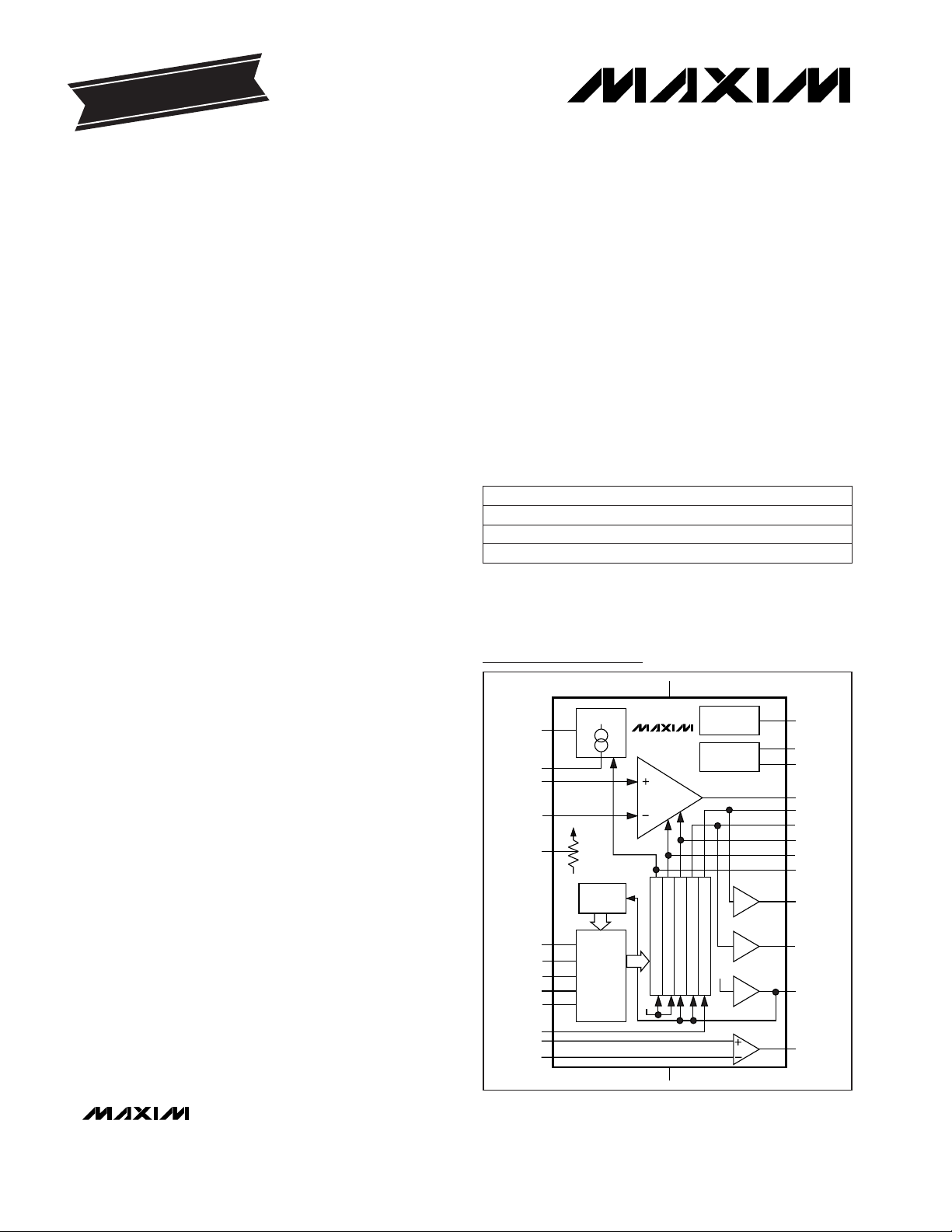
MAX1457
BIAS
GENERATOR
OSCILLATOR
16-BIT DAC - OFFSET TC
16-BIT DAC - OFFSET
16-BIT DAC - FSO
16-BIT DAC - FSO TC
16-BIT DAC - FSO LINEARITY
FSOTCDAC
OTCDAC
OFSTDAC
FSODAC
LINDAC
LINOUT
FSOTCOUT
VBBUF
V
BDRIVE
A = 1
A = 1
A = 1
AMPOUT
V
SS
VOUT
NBIAS
V
DD
FADJ
FOUT
SERIAL
EEPROM
INTERFACE
AGND
PGA
MCS
V
DD
ECS
ECLK
EDI
EDO
LINDACREF
AMP+
AMP-
BDRIVE
ISRC
INM
INP
V
SS
V
DD
12-BIT ADC
V
DD
19-1342; Rev 1; 8/98
PART
MAX1457CWI
MAX1457CCJ 0°C to +70°C
0°C to +70°C
TEMP. RANGE PIN-PACKAGE
28 Wide SO
32 TQFP
EVALUATION KIT
AVAILABLE
_______________Ordering Information
Ordering Information continued at end of data sheet.
Note:
Contact the factory for customized solutions.
*
Dice are tested at TA= +25°C.
Pin Configurations appear at end of data sheet.
MAX1457C/D 0°C to +70°C Dice*
Rail-to-Rail is a registered trademark of Nippon Motorola, Ltd.
SPI is a trademark of Motorola, Inc.
MicroWire is a trademark of National Semiconductor Corp.
Functional Diagram
Page 2

MAX1457
0.1%-Accurate Signal Conditioner
for Piezoresistive Sensor Compensation
2 _______________________________________________________________________________________
ABSOLUTE MAXIMUM RATINGS
ELECTRICAL CHARACTERISTICS
(VDD= +5V, VSS= 0V, TA= +25°C, unless otherwise noted.)
Stresses beyond those listed under “Absolute Maximum Ratings” may cause permanent damage to the device. These are stress ratings only, and functional
operation of the device at these or any other conditions beyond those indicated in the operational sections of the specifications is not implied. Exposure to
absolute maximum rating conditions for extended periods may affect device reliability.
Supply Voltage, VDDto VSS......................................-0.3V to +6V
All other pins....................................(V
SS
- 0.3V) to (VDD+ 0.3V)
Continuous Power Dissipation (T
A
= +70°C)
28-Pin Wide SO (derate 12.50mW/°C above +70°C) ..........1W
32-Pin TQFP (derate 11.1mW/°C above +70°C)...........889mW
Operating Temperature Ranges
MAX1457C_ _ ......................................................0°C to +70°C
MAX1457A_ _ .................................................-40°C to +125°C
Storage Temperature Range.............................-65°C to +150°C
Lead Temperature (soldering, 10sec).............................+300°C
Reference voltage = 5.000V
R
BIAS
= 400kΩ, f
CLK
= 100kHz (Note 1)
Gain = 54, DC to 10Hz, sensor impedance =
5kΩ, full-span output = 4V
V
OUT
= (VSS+ 0.25V) to (VDD- 0.25V)
(Note 5)
(Note 4)
5kΩ load to VSSor V
DD
From VSSto V
DD
f
CLK
= 100kHz, to 63% of final value
(Notes 2, 3)
CONDITIONS
µV200DAC Voltage Resolution
VVSS+ 1.3 VDD- 1.3V
ISRC
Current-Source Reference Input
Voltage Range
VVSS+ 1.3 VDD- 1.3V
BR
Bridge Voltage Swing
mA0.1 0.5 2.0I
BR
Bridge Current Range
%FSO0.0025Output Noise
mA
-1.0 1.0
(sink) (source)
Output Current Range
V
VSS+ 0.02 VDD- 0.02
Output Voltage Swing
ppm/°C±50Differential Signal Gain Tempco
V/V54 to 306Differential Signal Gain Range
mA2.0 2.6I
DD
Supply Current
V4.5 5 5.5V
DD
Supply Voltage
mV/V5 to 30
Input-Referred Adjustable
Full-Span Output Range
mV±100
Input-Referred Adjustable
Offset Range
dB90CMRRCommon-Mode Rejection Ratio
ms1Output Step-Response Time
MΩ
1
MΩ
1R
IN
Input Impedance
µV/°C±0.5Input-Referred Offset Tempco
%V
DD
0.01Amplifier Gain Nonlinearity
UNITSMIN TYP MAXSYMBOLPARAMETER
Output filter capacitor = 0.1µF, f
CLK
= 100kHz LSB2Differential Nonlinearity
Bits16DAC Resolution
VSS+ 0.25 VDD- 0.25
TA= T
MIN
to T
MAX
V/V49 54 60Minimum Differential Signal Gain
GENERAL CHARACTERISTICS
ANALOG INPUT (PGA)
ANALOG OUTPUT (PGA)
DIGITAL-TO-ANALOG CONVERTERS
CURRENT SOURCE
No load
Page 3

MAX1457
0.1%-Accurate Signal Conditioner
for Piezoresistive Sensor Compensation
_______________________________________________________________________________________ 3
Note 1: Circuit of Figure 5 with current source turned off. This value is adjustable through a bias resistor and represents the IC cur-
rent consumption. This excludes the 93C66 EEPROM average current, which is approximately 13µA at a refresh rate of 3Hz
(f
CLK
= 100kHz).
Note 2: Temperature errors for the entire range are compensated together with the sensor errors.
Note 3: The sensor and the MAX1457 must always be at the same temperature during calibration and use.
Note 4: This is the maximum allowable sensor offset at minimum gain (54V/V).
Note 5: This is the sensor’s sensitivity normalized to its drive voltage, assuming a desired full-span output of 4V and a bridge volt-
age of 2.5V. Lower sensitivities can be accommodated by using the auxiliary op amp. Higher sensitivities can be accommodated by operating at lower bridge voltages.
ELECTRICAL CHARACTERISTICS (continued)
(VDD= +5V, VSS= 0V, TA= +25°C, unless otherwise noted.)
VBR= 2.5V to 3.5V, f
CLK
= 100kHz
V
OUT
= (VSS+ 0.25V) to (VDD- 0.25V)
(VIN- V
OUT
) at VIN= 2.5V,
R
BIAS
= 400kΩ (no load)
5kΩ load to VSSor V
DD
R
BIAS
= 400kΩ, VIN= 2.5V (no load)
R
BIAS
= 400kΩ, VIN= 2.5V,
V
OUT
= 2.5V ±20mV
f
CLK
= 100kHz
R
BIAS
= 400kΩ
R
BIAS
= 400kΩ (no load)
CONDITIONS
mA
-1.0 1.0
(sink) (source)
Output Current Range
V
VSS+ 0.02 VDD- 0.02
Output Voltage Swing
mV-20 20
Offset Voltage (as unity-gain
follower)
dB60A
V
Open-Loop Gain
VVSS+ 1.3 VDD- 1.2CMR
Input Common-Mode
Voltage Range
LSB2ADC Differential Nonlinearity
mV-20 20V
OFS
Offset Voltage
µA-50 50Current Drive
ms160Conversion Time
Bits12ADC Resolution
VVSS+ 1.3 VDD- 1.3Voltage Swing
UNITSMIN TYP MAXSYMBOLPARAMETER
VSS+ 0.25 VDD- 0.25
ANALOG-TO-DIGITAL CONVERTER
UNCOMMITTED OP AMP
OUTPUTS (LINDAC, FSOTCDAC)
No load
Page 4

MAX1457
0.1%-Accurate Signal Conditioner
for Piezoresistive Sensor Compensation
4 _______________________________________________________________________________________
______________________________________________________________Pin Description
1 28
Positive Sensor Input. Input impedance >1MΩ. Rail-to-rail input range.
2 29
Negative Sensor Input. Input impedance >1MΩ. Rail-to-rail input range.
3 30 Positive Input of General-Purpose Operational Amplifier
4 31 Negative Input of General-Purpose Operational Amplifier
—
4, 16,
22, 32
Not internally connected.
7 3
PGA Output Voltage. Connect a 0.1µF capacitor from VOUT to VSS. High impedance when
MCS is low.
6 2 Sensor Excitation Current. This pin drives a nominal 0.5mA through the sensor.
5 1 Output of General-Purpose Operational Amplifier. High impedance when MCS is low.
12 9 Reference Input to FSO Linearity DAC. Normally tied to VOUT.
11 8
Buffered FSO Linearity DAC Output. Use a resistor (R
LIN
) greater than 100kΩ, from LINOUT
to ISRC to correct second order FSO nonlinearity errors. Leave unconnected if not
correcting second order FSO nonlinearity errors.
10 7 Buffered Bridge Voltage (the voltage at BDRIVE). Leave unconnected if unused.
9 6
Buffered FSO TC DAC Output. Tie to ISRC with a resistor (R
STC
≥ 50kΩ).
8 5
Current-Source Reference. Connect a 50kΩ resistor from ISRC to VSS.
INP
INM
AMP+
AMP-
N.C.
VOUT
BDRIVE
AMPOUT
LINDACREF
LINOUT
VBBUF
FSOTCOUT
ISRC
13 10 FSO Linearity DAC Output Voltage. Connect 0.1µF capacitor from LINDAC to VSS.LINDAC
14 11 Negative Power Supply InputV
SS
15 12 OFFSET TC DAC Output Voltage. Connect a 0.1µF capacitor from OTCDAC to VSS.OTCDAC
16 13 FSO DAC Output Voltage. Connect a 0.1µF capacitor from FSODAC to VSS.FSODAC
17 14 FSO TC DAC Output Voltage. Connect a 0.1µF capacitor from FSOTCDAC to VSS.FSOTCDAC
18 15 OFFSET DAC Output Voltage. Connect a 0.1µF capacitor from OFSTDAC to VSS.OFSTDAC
19 17
Serial Input (data from EEPROM), active high. CMOS logic-level input pin through which the
MAX1457’s internal registers are updated with EEPROM coefficients. Disabled when MCS is
low.
EDO
20 18
Serial Output (data to EEPROM), active high. CMOS logic-level output pin through which
the MAX1457 gives external commands to the EEPROM. Temperature-compensation data
is available through this pin. Becomes high impedance when MCS is low.
EDI
21 19 CMOS Logic-Level Clock Output for external EEPROM. High impedance when MCS is low.ECLK
22 20
Chip-Select Output for external EEPROM. CMOS logic-level output pin through which the
MAX1457 enables/disables EEPROM operation. High impedance when MCS is low.
ECS
23 21 Frequency Output. Internal oscillator output signal. Normally left open.FOUT
24 23
Frequency Adjust. Connect to VSSwith a 1.5MΩ resistor (R
OSC
) to set internal oscillator fre-
quency to 100kHz. Connect a 0.1µF bypass capacitor from FADJ to V
SS
.
FADJ
PIN
FUNCTIONNAME
25 24
Master Chip Select. The MAX1457 is selected when MCS is high. Leave unconnected for
normal operation (internally pulled up to VDDwith 1MΩ resistor). External 5kΩ pull-up may
be required in noisy environments.
MCS
26 25
Bias Setting Pin. Connect to VDDwith a 400kΩ resistor (R
BIAS
). Connect a 0.1µF bypass
capacitor from NBIAS to V
SS
.
NBIAS
27 26 Mid-Supply Reference for Analog Circuitry. Connect a 0.1µF capacitor from VSSto AGND.AGND
28 27 Positive Power-Supply Input. Connect a 0.1µF capacitor from VDDto VSS.V
DD
TQFPSO
Page 5

MAX1457
0.1%-Accurate Signal Conditioner
for Piezoresistive Sensor Compensation
_______________________________________________________________________________________ 5
_______________Detailed Description
The MAX1457 provides an analog amplification path for
the sensor signal and a digital path for calibration and
temperature correction. Calibration and correction are
achieved by varying the offset and gain of a programmable-gain amplifier (PGA) and by varying the sensor
bridge current. The PGA utilizes a switched-capacitor
CMOS technology, with an input-referred offset trimming range of ±100mV (20mV/V) and an approximate
3µV (input referred, at minimum gain of 54V/V) resolution (16 bits). The PGA provides eight gain values from
54V/V to 306V/V. The bridge current source is programmable from 0.1mA to 2mA, with a 15nA step size.
The MAX1457 uses five 16-bit DACs with calibration
coefficients stored in a low-cost external EEPROM. This
memory (an external 4096-bit EEPROM) contains the
following calibration coefficients as 16-bit words:
• FSO (full-span output)
• FSO TC (including nonlinearities)
• Offset
• Offset TC (including nonlinearities)
• Pressure nonlinearity
Figure 1 shows a typical pressure-sensor output and
defines the offset, full-scale, and full-span output values
as a function of voltage.
Offset Correction
Initial offset calibration is accomplished by reading a
16-bit word (coefficient) from the EEPROM and writing it
to the OFFSET DAC. The resulting voltage (OFSTDAC)
is fed into a summing junction at the PGA output for
compensating the sensor offset with a resolution of
±0.2mV (±0.005% FSO).
VOLTAGE
PRESSURE
FULL-SCALE (FS)
FULL-SPAN OUTPUT (FSO)
OFFSET
Figure 1. Typical Pressure-Sensor Output
V
BR
T
V
BR
I
BR
R
STC
V
DD
EDIECS
ECLK
TO/FROM
EXTERNAL EEPROM
EDO
EEPROM
INTERFACE
ADC
BDRIVE
12 16
OUTPUT
PGA
TEMPERATURE-
DEPENDENT VOLTAGE
OFFSET TC
DAC REFERENCE VOLTAGE
FSO TC
DAC
Σ
16
A = 1
Figure 2. Simplified Diagram of Temperature Error Correction
Page 6

MAX1457
FSO Calibration
Two adjustments are required for FSO calibration. First
set the coarse gain by digitally selecting the PGA gain.
Then calibrate the bridge current by writing a 16-bit
calibration coefficient word to the FSO DAC. These two
adjustments result in a calibration resolution of ±0.2mV
(±0.005% FSO).
Linear Temperature Compensation
Temperature errors are compensated by writing 16-bit
calibration coefficients into the OFFSET TC DAC and
the FSO TC DAC (changing the current-source value
through resistive feedback from the FSOTCDAC pin to
the ISRC pin). The piezoresistive sensor is powered by
a current source resulting in a temperature-dependent
bridge voltage. The reference inputs of the OFFSET TC
DAC and FSO TC DAC are connected to the bridge
voltage. For a fixed digital word, the DAC output voltages track the bridge voltage as it varies with temperature (quasi-linearly).
Multislope Temperature Compensation
The MAX1457 utilizes multislope temperature compensation, allowing for compensation of arbitrary error
curves restricted only by the available adjustment
range and the shape of the temperature signal.
The MAX1457 offers a maximum of 120 calibration
points (each consisting of one OFFSET TC coefficient
and one FSO TC coefficient) over the operating temperature range. Each 16-bit calibration coefficient provides
compensation of the output (either offset or FSO) with
±0.2mV (0.005% FSO) resolution. A 12-bit ADC measures the temperature-dependent bridge voltage
(BDRIVE) and selects (by addressing the EEPROM) the
corresponding offset and FSO calibration data within a
specific narrow temperature span (e.g., ≅ 1°C). The
120-segment compensation enables the MAX1457 to
compensate temperature errors for a broad range of
sensors (Figure 2).
Calculate the correction coefficients by curve-fitting to
sensor-error test data. More test points allow for better
curve-fit accuracy but result in increased test overhead. The remaining error is further affected by the
slope of the temperature errors. For example, correcting a 6% nonlinearity over temperature with 60 segments (half of the available calibration points) with
perfect curve fitting yields an error on the order of 0.1%
(6%/60). Figure 3 illustrates this compensation.
0.1%-Accurate Signal Conditioner
for Piezoresistive Sensor Compensation
6 _______________________________________________________________________________________
PRESSURE
PRESSURE
PRESSURE
TEMPERATURE
a) UNCOMPENSATED SENSOR ERROR
SMALL
NONLINEARITY ERROR
TEMPERATURE
b) RESULTANT ERROR AFTER LINEAR COMPENSATION
SMALL
NONLINEARITY ERROR
TEMPERATURE
c) RESULTANT ERROR AFTER MULTISLOPE COMPENSATION
Figure 3. Multislope Temperature Compensation
Page 7

Pressure Nonlinearity Correction
The MAX1457 corrects pressure nonlinearity in an analog fashion by providing a resistive feedback path
(resistor R
LIN
in Figure 4) from a buffered main output
(LINOUT pin) to the current source (ISRC pin). The
feedback coefficient is then set by writing a 16-bit word
to the FSO LIN DAC.
For many silicon sensors, this type of nonlinearity correction may reduce sensor nonlinearity by an order of
magnitude.
_____________Applications Information
Ratiometric Output Configuration
Ratiometric output configuration provides an output that
is proportional to the power-supply voltage. When used
with ratiometric ADCs, this output provides digital pressure values independent of supply voltage.
The MAX1457 has been designed to provide a highperformance ratiometric output with a minimum number
of external components (Figure 5). These external components typically include an external EEPROM (93C66),
decoupling capacitors, and resistors.
2-Wire, 4–20mA Configuration
In this configuration, a 4mA current is used to power a
transducer, and an incremental current of 0 to 16mA
proportional to the measured pressure is transmitted
over the same pair of wires. Current output enables
long-distance transmission without a loss of accuracy
due to cable resistance.
Only a few components (Figure 6) are required to build
a 4–20mA output configuration. A low-quiescent-current voltage regulator with a built-in bandgap reference
(such as the REF02) should be used. Since the
MAX1457 performs temperature and gain compensation of the circuit, the temperature stability and calibration accuracy of the reference voltage is of secondary
importance.
The external transistor forms the controllable current
loop. The MAX1457 controls the voltage across resistor
R
A
. With RA= 50Ω, a 0.2V to 1.0V range would be
required during the calibration procedure. If needed,
the PGA output can be divided using resistors RBand
RC.
For overvoltage protection, place a Zener diode across
V
IN-
and V
IN+
(Figure 6). A feedthrough capacitor
across the inputs reduces EMI/RFI.
Test System Configuration
The MAX1457 is designed to support an automated
production pressure-temperature test system with integrated calibration and temperature compensation.
Figure 7 shows the implementation concept for a lowcost test system capable of testing up to five transducer modules connected in parallel. Three-state outputs
on the MAX1457 allow for parallel connection of transducers.
The test system shown in Figure 7 includes a dedicated
test bus consisting of six wires (the capacitive loading
of each transducer module should not exceed the
EEPROM fan-out specifications):
• Two power-supply lines
• One analog output voltage line from the transducers
to a system digital voltmeter
• Three MicroWire/SPI interface lines: EDI (data-in),
EDO (data-out), and ECLK (clock)
For simultaneous testing of more than five transducer
modules, use buffers to prevent overloading the data bus.
A digital multiplexer controls the two chip-select signals
for each transducer:
• Module Select (MCS) places the selected module
into an active state, enabling operation and compensation
• EEPROM Select (ECS) enables writing to the trans-
ducer’s EEPROM
MAX1457
0.1%-Accurate Signal Conditioner
for Piezoresistive Sensor Compensation
_______________________________________________________________________________________ 7
V
BR
V
OUT
I
BR
R
LIN
V
DD
PGA
FSO
LIN
DAC
111...1
16 BIT
Figure 4. Pressure Nonlinearity Correction
Page 8

MAX1457
Sensor Compensation Overview
Compensation requires an examination of the sensor
performance over the operating pressure and temperature range. Use two test pressures (e.g., zero and fullspan) and two temperatures. More test pressures and
temperatures will result in greater accuracy. A simple
compensation procedure can be summarized as follows:
Set reference temperature (e.g., +25°C):
1) Initialize each transducer by loading its EEPROM with
default coefficients (e.g., based on mean values of
offset, FSO, and bridge resistance) to prevent gross
overload of the MAX1457.
2) Set the initial bridge voltage (with the FSO DAC) to
half the supply voltage. The bridge voltage can be
measured by the MAX1457 and returned to the test
computer via the serial interface or by using the system digital voltmeter to measure the voltage on either
BDRIVE or VBBUF.
3) Calibrate the transducer’s output offset and FSO
using the OFFSET and FSO DACs, respectively.
4) Store calibration data in the test computer.
Set next test temperature:
5) Calibrate offset and FSO using the OFFSET TC and
FSO TC DACs, respectively.
6) Store calibration data in the test computer.
Repeat steps 5 and 6 for each required test temperature.
0.1%-Accurate Signal Conditioner
for Piezoresistive Sensor Compensation
8 _______________________________________________________________________________________
MAX1457
CURRENT
SOURCE
BIAS
GENERATOR
OSCILLATOR
16-BIT DAC - OFFSET TC
16-BIT DAC - OFFSET
16-BIT DAC - FSO
16-BIT DAC - FSO TC
16-BIT DAC - FSO LIN
FSOTCDAC
OTCDAC
OFSTDAC
FSODAC
LINDAC
LINOUT
FSOTCOUT
VBBUF
A = 1
A = 1
V
BDRIVE
V
DD
A = 1
OP AMP
AMPOUT
V
SS
VOUT
NBIAS
R
OSC
1.5M
0.1µF
0.1µF
0.1µF
5 x 0.1µF
R
BIAS
400k
V
DD
FADJ
FOUT
SERIAL
EEPROM
INTERFACE
12-BIT ADC
AGND
SENSOR
0.1µF
+5V
+5V
V
DD
V
SS
5k*
+5V
0.1µF
0.1µF
*OPTIONAL PULL-UP RESISTOR
MCS
ECS
ECLK
EDI
EDO
LINDACREF
AMP+
AMP-
CS
CLK
DI
DO
V
DD
EEPROM
93C66 SO-8
ORG
V
SS
BDRIVE
ISRC
R
ISRC
50k
PGA
V
DD
R
STC
R
LIN
(OPTIONAL)
INM
INP
VOUT
Figure 5. Basic Ratiometric Output Configuration
Page 9

MAX1457
0.1%-Accurate Signal Conditioner
for Piezoresistive Sensor Compensation
_______________________________________________________________________________________ 9
MAX1457
BIAS
GENERATOR
OSCILLATOR
16-BIT DAC - OFFSET TC
16-BIT DAC - OFFSET
16-BIT DAC - FSO
16-BIT DAC - FSO TC
16-BIT DAC - FSO LIN
FSOTCDAC
OTCDAC
OFSTDAC
FSODAC
LINDAC
LINOUT
FSOTCOUT
VBBUF
V
BDRIVE
R
B
R
D
OPTIONAL FEEDTHROUGH
CAPACITOR FOR
EMI/RFI PROTECTION
A = 1
A = 1
A = 1
OP AMP
AMPOUT
V
SS
R
C
R
OFST
VOUT
NBIAS
R
OSC
1.5M
R
A
50Ω
(TYP)
0.1µF
0.1µF
0.1µF
5 x 0.1µF
R
BIAS
400k
V
DD
FADJ
FOUT
SERIAL
EEPROM
INTERFACE
12-BIT ADC
AGND
SENSOR
0.1µF
0.1µF
*OPTIONAL PULL-UP RESISTOR
MCS
ECS
ECLK
EDI
EDO
LINDACREF
AMP+
AMP-
+5V
V
SS
EEPROM
93C66 SO-8
BDRIVE
ISRC
10µF
R
ISRC
50k
R
STC
50Ω
R
LIN
(OPTIONAL)
INM
0.1µF
INP
PGA
V
DD
VIN
VIN+
GND
REF02
VOUT
VIN-
CS
+5V
5k*
CLK
DI
DO
V
DD
ORG
V
SS
Figure 6. Basic 2-Wire 4–20mA Configuration
Page 10

MAX1457
7) Perform curve-fitting to test data.
8) Based on a curve-fit algorithm, calculate up to 120
sets of offset and FSO correcting values.
9) Download correction coefficients to transducer
EEPROM.
10) Perform a final test.
The resulting transducer temperature errors are limited by
the following factors:
• Number of selected segments for compensation (up to
120).
• Accuracy of the curve fitting, which depends on the
algorithm used, the number of test temperatures, and
the sensor temperature error’s shape.
• Repeatability of the sensor performance. This will limit
the MAX1457’s accuracy.
Sensor Calibration and
Compensation Example
Calibration and compensation requirements for a sensor involve conversion of the sensor-specific performance into a normalized output curve. An example of
the MAX1457’s capabilities is shown in Table 1.
As shown in Table 1, a repeatable piezoresistive sensor
with an initial offset of 16.4mV and FSO of 55.8mV was
converted into a compensated transducer (utilizing the
piezoresistive sensor with the MAX1457) with an offset
of 0.500V and a span of 4.000V. Nonlinear sensor offset
and FSO temperature errors, which were on the order
of 4% to 5% FSO, were reduced to under ±0.1% FSO.
The graphs in Figure 8 show the output of the uncompensated sensor and the output of the compensated
transducer.
0.1%-Accurate Signal Conditioner
for Piezoresistive Sensor Compensation
10 ______________________________________________________________________________________
MAX1457
EDO
V
OUT
V
DD
MCS
MODULE 1
EEPROM
EDI
ECLK
ECS
V
SS
V
SS
V
DD
V
DD
V
SS
TEST
OVEN
MAX1457
EDO
V
OUT
MCS
MODULE 2
EEPROM
EDI
ECLK
EDI
EDO
VOUT
DIGITAL
MULTIPLEXER
+5V
ECS1
ECS[1:N], MCS[1:N]
ECS2MCS1
MCS2
ECS N MCS N
ECLK
ECS
MAX1457
EDO
V
OUT
MCS
MODULE N
EEPROM
EDI
ECLK
ECS
• • •
• • •
• • •
• • •
• • •
• • •
• • •
DVM
Figure 7. Automated Test System Concept
Page 11

______________________________________________________________________________________ 11
MAX1457
0.1%-Accurate Signal Conditioner
for Piezoresistive Sensor Compensation
V
OUT
(mV)
V
OUT
(V)
PRESSURE (kPa)
UNCOMPENSATED RAW SENSOR OUTPUT
0
40
80
120
160
0 4020 60 80 100
PRESSURE (kPa)
0 4020 60 80 100
COMPENSATED TRANSDUCER
0
1
2
3
4
5
ERROR (% FSO)
ERROR (% FSO)
TEMPERATURE (°C)
UNCOMPENSATED SENSOR TEMPERATURE ERROR
-20
-10
10
0
20
30
-50 50
FSO
FSO
0 100 150 -50 500 100 150
TEMPERATURE (°C)
COMPENSATED TRANSDUCER ERROR
-0.15
-0.10
-0.05
0
0.05
0.10
0.15
OFFSET
TA = +25°C
17mV ≤ V
OUT
≤ 73mV
TA = +25°C
0.5V ≤ V
OUT
≤ 4.5V
OFFSET
Figure 8. Comparison of an Uncompensated Sensor (left) and a Compensated Transducer (right)
Typical Uncompensated Input (Sensor)
Offset . . . . . . . . . . . . . . . . . . . . . . . . . .±100% FSO
FSO . . . . . . . . . . . . . . . . . . . . . .20mV/V to 30mV/V
Offset TC . . . . . . . . . . . . . . . . . . . . . . . . .20% FSO
Offset TC Nonlinearity . . . . . . . . . . . . . . . .4% FSO
FSO TC . . . . . . . . . . . . . . . . . . . . . . . . . .-20% FSO
FSO TC Nonlinearity . . . . . . . . . . . . . . . . . .5% FSO
Typical Compensated Transducer Output
Temperature Range . . . . . . . . . . .-40°C to +125°C
V
OUT
. . . . . . . . . . . . . . . .ratiometric to VDDat 5.0V
Offset at +25°C . . . . . . . . . . . . . . .0.500V ± 200µV
FSO at +25°C . . . . . . . . . . . . . . . . .4.000V ±200µV
Offset Accuracy Over
Temperature Range . . . . . . . . . .±4mV (0.1% FSO)
FSO Accuracy Over
Temperature Range . . . . . . . . ..±4mV (0.1% FSO)
Table 1. MAX1457 Sensor Calibration and Compensation
Page 12

MAX1457 Evaluation
___________________ Development Kit
To expedite the development of MAX1457-based transducers and test systems, Maxim has produced a
MAX1457 evaluation kit (EV kit). First-time users of the
MAX1457 are strongly encouraged to use this kit.
The kit is designed to facilitate manual programming of
the MAX1457 with a sensor. It includes the following:
1) Evaluation board (EV board) with a silicon pressure
sensor, ready for customer evaluation.
2) Design/applications manual, which describes in detail
the architecture and functionality of the MAX1457.
This manual was developed for test engineers familiar
with data acquisition of sensor data and provides
sensor-compensation algorithms and test procedures.
3) MAX1457 communication software, which enables
programming of the MAX1457 from a computer keyboard (IBM compatible), one module at a time.
4) Interface adapter and cable, which allows the connection of the EV board to a PC parallel port.
MAX1457
0.1%-Accurate Signal Conditioner
for Piezoresistive Sensor Compensation
Maxim cannot assume responsibility for use of any circuitry other than circuitry entirely embodied in a Maxim product. No circuit patent licenses are
implied. Maxim reserves the right to change the circuitry and specifications without notice at any time.
12
____________________Maxim Integrated Products, 120 San Gabriel Drive, Sunnyvale, CA 94086 408-737-7600
© 1998 Maxim Integrated Products Printed USA is a registered trademark of Maxim Integrated Products.
TRANSISTOR COUNT: 17534
SUBSTRATE CONNECTED TO V
SS
Chip Information
Ordering Information (continued)
Pin Configurations
PART
MAX1457AWI
MAX1457ACJ -40°C to +125°C
-40°C to +125°C
TEMP. RANGE PIN-PACKAGE
28 Wide SO
32 TQFP
TOP VIEW
TOP VIEW
AMP-
AMP+
INM
293031
MAX1457
SS
OTCDAC
TQFP
INP
28
13
FSODAC
VDDAGND
27
14
FSOTCDAC
26
15
OFSTDAC
25
1611 12
NBIAS
N.C.
24 MCS
FADJ
23
22
N.C.
21
FOUT
20
ECS
19
ECLK
18
EDI
17
EDO
INP
INM
AMP+
AMP-
AMPOUT
BDRIVE
VOUT
ISRC
FSOTCOUT
VBBUF
LINOUT
LINDACREF
LINDAC
V
28
27
26
25
24
23
22
21
20
19
18
17
16
15
V
DD
AGND
NBIAS
MCS
FADJ
FOUT
ECS
ECLK
EDI
EDO
OFSTDAC
FSOTCDAC
FSODAC
OTCDAC
BDRIVE
VOUT
N.C.
ISRC
FSOTCOUT
VBBUF
1
2
3
4
5
MAX1457
6
7
8
9
10
11
12
13
14
SS
N.C.
32
1AMPOUT
2
3
4
5
6
7
8LINOUT
10
9
V
LINDAC
LINDACREF
SO
 Loading...