

Page 1
General Description
The MAX13410E–MAX13415E are half-duplex RS-485-/RS422-compatible transceivers optimized for isolated applications. These devices feature an internal low-dropout
regulator (LDO), one driver, and one receiver. The internal LDO allows the part to operate from an unregulated
power supply of up to 28V. The AutoDirection feature
reduces the number of optical isolators needed in isolated applications. Other features include enhanced ESD
protection, fail-safe circuitry, slew-rate limiting, and fullspeed operation.
The MAX13410E–MAX13415E internal LDO generates a
5V ±10% power supply that is used to power its internal
circuitry. The MAX13412E–MAX13415E bring the 5V to an
output V
REG
that allows the user to power additional
external circuitry with up to 20mA to further reduce external components. The MAX13410E/MAX13411E do not
have a 5V output and come in industry-compatible
pinouts. This allows easy replacement in existing designs.
The MAX13410E–MAX13415E feature a 1/8-unit load
receiver input impedance, allowing up to 256 transceivers on the bus. All driver outputs are ESD protected
using the Human Body Model. These devices also
include fail-safe circuitry (MAX13410E/MAX13411E/
MAX13414E/MAX13415E only), guaranteeing a logichigh receiver output when the receiver inputs are open
or shorted. The receiver outputs a logic-high when the
transmitter on the terminated bus is disabled (high
impedance).
The MAX13412E/MAX13413E feature Maxim’s proprietary AutoDirection control. This architecture eliminates
the need for the DE and RE control signals. In isolated
applications, this reduces the cost and size of the system by reducing the number of optical isolators required.
The MAX13410E/MAX13412E/MAX13414E feature
reduced slew-rate drivers that minimize EMI and reduce
reflections caused by improperly terminated cables,
allowing error-free transmission up to 500kbps. The
MAX13411E/MAX13413E/MAX13415E are not slew-rate
limited, allowing transmit speeds up to 16Mbps.
The MAX13410E–MAX13415E are available in an 8-pin
SO package with an exposed paddle to improve power
dissipation, and operate over the extended -40°C to
+85°C temperature range.
Features
♦ Wide +6V to +28V Input Supply Range
♦ +5V Output Supplies Up to 20mA to External
Circuitry
♦ Internal LDO
♦ Low 65µA (typ) Shutdown Supply Current
♦ Extended ESD Protection
±15kV Human Body Model (MAX13412E/
MAX13413E)
±14kV Human Body Model (MAX13410E/
MAX13411E)
♦ 1/8-Unit Load, Allowing Up to 256 Transceivers on
the Bus
♦ -40°C to +85°C Operating Temperature Range
♦ Fail-Safe
♦ Slew-Rate Limited and Full-Speed Versions
♦ Up to 16Mbps Data Rate on Full-Speed Versions
Applications
-
MAX13410E–MAX13415E
RS-485 Transceiver with Integrated Low-Dropout
Regulator and AutoDirection Control
________________________________________________________________
Maxim Integrated Products
1
19-1058; Rev 1; 8/09
For pricing, delivery, and ordering information, please contact Maxim Direct at 1-888-629-4642,
or visit Maxim’s website at www.maxim-ic.com.
Ordering Information/Selector Guide
Note: All devices operate over the -40°C to +85°C operating
temperature range.
+
Denotes a lead(Pb)-free/RoHS-compliant package.
*
EP = Exposed pad.
Ordering Information/Selector Guide continued at end of data
sheet.
Isolated RS-485 Interfaces
Utility Meters
Industrial Equipment
Telecomm Equipment
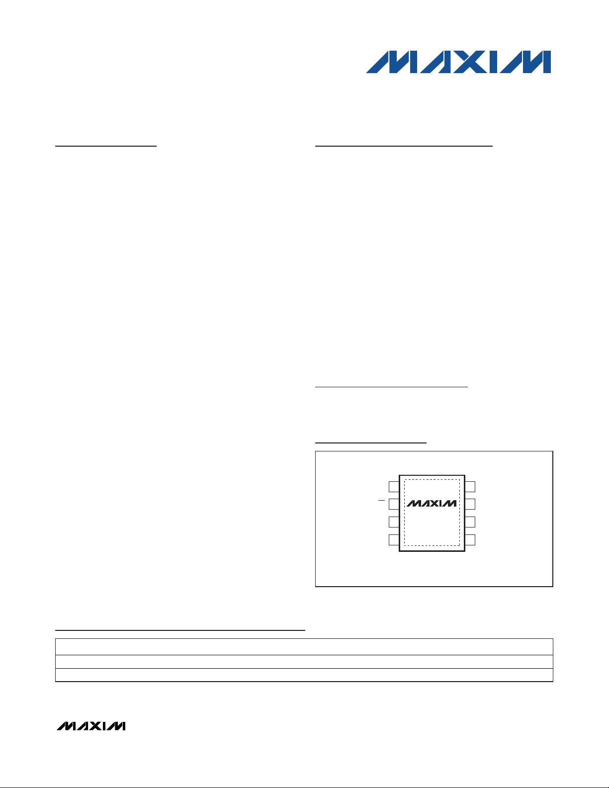
Pin Configurations
Pin Configurations continued at end of data sheet.
TOP VIEW
1
RO
+
87V
CC
2
MAX13410E
3
DE
4
MAX13411E
*EP
BRE
A
6
GNDDI
5
*EXPOSED PAD CONNECTED TO GROUND
SO
PART PIN-PACKAGE AutoDirection DATA RATE (max) 5V LDO OUTPUT
MAX13410EESA+ 8 SO-EP* No 500 kbps No
MAX13411EESA+ 8 SO-EP* No 16Mbps No
Page 2
MAX13410E–MAX13415E
RS-485 Transceiver with Integrated Low-Dropout
Regulator and AutoDirection Control
2 _______________________________________________________________________________________
ABSOLUTE MAXIMUM RATINGS
Stresses beyond those listed under “Absolute Maximum Ratings” may cause permanent damage to the device. These are stress ratings only, and functional
operation of the device at these or any other conditions beyond those indicated in the operational sections of the specifications is not implied. Exposure to
absolute maximum rating conditions for extended periods may affect device reliability.
(All voltages referenced to GND.)
V
CC
.........................................................................-0.3V to +30V
RE, DE/RE, DE, DI, RO, V
REG
..................................-0.3V to +6V
A, B............................................................................-8V to +13V
Short-Circuit Duration (RO, A, B) to GND ................. Continuous
Continuous Power Dissipation (T
A
= +70°C)
8-Pin SO-EP (derate 19.2mW/°C above +70°C) ........1539mW
Operating Temperature Range ...........................-40°C to +85°C
Storage Temperature Range ............................-65°C to +150°C
Junction Temperature......................................................+150°C
θ
JA
(Note 1)...................................................................52.0°C/W
θ
JC
(Note 1).....................................................................6.0°C/W
Lead Temperature (soldering, 10s) ................................+300°C
Note 1: Package thermal resistances were obtained using the method described in JEDEC specificactions JESD51-7 using a four layer board.
For detailed information on package consitencies refer to www.maxim-ic/thermal-tutorial.
ELECTRICAL CHARACTERISTICS
(VCC= +6.0V to +28V, TA= T
MIN
to T
MAX
, unless otherwise noted. Typical values are at VCC= +7.5V, CS= 1µF, and TA= +25°C.) (Note 2)
Supply Voltage V
LDO Output Voltage V
LDO Output Current I
LDO Dropout Voltage V
PARAMETER SYMBOL CONDITIONS MIN TYP MAX UNITS
Minimum Bypass Capacitor on V
Supply Current I
Shutdown Current I
Thermal-Shutdown Threshold T
Thermal-Shutdown Threshold
Hysteresis
DRIVER
Change in Magnitude of Differential
Output Voltage
Driver Common-Mode Output Voltage V
Change In Magnitude of CommonMode Voltage
Input High Voltage V
Input Low Voltage V
Input Current I
Driver-Disable Threshold V
(Note 3) 6.0 28.0 V
CC
VCC = +7.5V, I
VCC = +28V, I
VCC > +7.5V 20
VCC = +5V, I
DO
Guaranteed by design,
S
MAX13412E–MAX13415E
RE, DE = high/no load
(MAX13410E/MAX13411E)
CC
RE, DE/RE = high, DI = low/no load
(MAX13412E–MAX13415E)
DE = low, RE = high
(MAX13410E/MAX13411E)
TS
R
= 100Ω, Figure 1 2.0 5.5
DIFF
R
= 54Ω, Figure 1 1.5 5.5Differential Driver Output V
OD
OD
OC
OC
IH
IL
IN
DT
DIFF
No load 5.5
R
= 100Ω or 54Ω, Figure 1 0.2 V
DIFF
R
= 100Ω or 54Ω, Figure 1 1 3 V
DIFF
R
= 100Ω or 54Ω, Figure 1 0.2 V
DIFF
DI, DE, RE, DE/RE 2.0 V
DI, DE, RE, DE/RE 0.8 V
DI, DE, RE, DE/RE ±1 µA
TA = +25°C (MAX13412E/MAX13413E) 0.6 1.0 V
REG
REG
REG
C
SHDN
T
TSH
ΔV
ΔV
= 20mA 4.5 5 5.5
LOAD
= 0mA 4.5 5 5.5
LOAD
= 20mA 0.5 V
OUT
1µF
10
10
45 µA
+150 °C
15 °C
V
mA
mA
V
Page 3
MAX13410E–MAX13415E
RS-485 Transceiver with Integrated Low-Dropout
Regulator and AutoDirection Control
_______________________________________________________________________________________ 3
SWITCHING CHARACTERISTICS–MAX13410E
(VCC= +6.0V to +28V, TA= T
MIN
to T
MAX
, unless otherwise noted. Typical values are at VCC= +7.5V, CS= 1µF, and TA= +25°C.) (Note 2)
)
)
ELECTRICAL CHARACTERISTICS (continued)
(VCC= +6.0V to +28V, TA= T
MIN
to T
MAX
, unless otherwise noted. Typical values are at VCC= +7.5V, CS= 1µF, and TA= +25°C.) (Note 2)
PARAMETER SYMBOL CONDITIONS MIN TYP MAX UNITS
Driver Short-Circuit Output Current I
Driver Short-Circuit-Foldback Output
Current
RECEIVER
Input Current (A and B) I
Receiver Differential Threshold
Voltage
Receiver Input Hysteresis ΔV
Output High Voltage V
Output Low Voltage V
Thr ee- S tate O utp ut C ur r ent at Recei ver I
Receiver-Input Resistance R
Receiver-Output Short-Circuit Current I
ESD PROTECTION
ESD Protection (A, B)
ESD Protection (A, B)
ESD Protection (All Other Pins) Human Body Model ±2
OSD
I
OSDF
A, B
V
TH
OH
OL
OZR
OSR
0V < V
-7V < V
(VCC - 1V) < V
-7V < V
RE, DE, DE/RE =
GND, V
-7V < VCM < +12V
(MAX13410E/MAX13411E)
-7V < VLM < +12V
(MAX13412E/MAX13413E)
VA + VB = 0V 15 mV
TH
IO = -1mA, VA - VB > V
IO = +1mA, VA - VB < -V
0 < VO < V
-7V < VCM < +12V 96 kΩ
IN
0V < VRO < V
< +12V +250
OUT
< 0V -250
OUT
< +12V 20
OUT
< 0V -20
OUT
VIN = +12V 125
CC
= GND
V
= -7V -100
IN
-200 -50
-100 100
V
TH
TH
REG
REG
- 0.6 V
REG
±8 ±95
Human Body Model
(MAX13412E/MAX13413E)
Human Body Model
(MAX13410E/MAX13411E)
mA
mA
µA
mV
0.4 V
0.01 ±1 µA
mA
±15 kV
±14 kV
kV
PARAMETER SYMBOL CONDITIONS MIN TYP MAX UNITS
DRIVER
Driver Propagation Delay
Driver Differential Output
Rise or Fall Time
Driver Differential Output Skew
- t
|t
DPLH
DPHL
|
Maximum Data Rate f
Driver Enable from Shutdown to
Output High
Driver Enable from Shutdown to
Output Low
t
DPLH
t
DPHL
t
HL
t
LH
t
DSKEW
MAX
t
DZH(SHDN
t
DZL(SHDN
R
= 54Ω, CL = 50pF,
DIFF
Figures 2a and 3a
R
= 54Ω, CL = 50pF,
DIFF
Figures 2a and 3a
R
= 54Ω, CL = 50pF,
DIFF
Figures 2a and 3a
S2 closed, Figure 4,
R
= 500Ω, CL = 100pF
L
S2 closed, Figure 4,
R
= 500Ω, CL = 100pF
L
150 1000
150 1000
250 900
250 900
ns
ns
140 ns
500 kbps
11 µs
6µs
Page 4
MAX13410E–MAX13415E
RS-485 Transceiver with Integrated Low-Dropout
Regulator and AutoDirection Control
4 _______________________________________________________________________________________
)
)
SWITCHING CHARACTERISTICS–MAX13411E
(VCC= +6.0V to +28V, TA= T
MIN
to T
MAX
, unless otherwise noted. Typical values are at VCC= +7.5V, CS= 1µF, and TA= +25°C.) (Note 2)
)
)
SWITCHING CHARACTERISTICS–MAX13410E (continued)
(VCC= +6.0V to +28V, TA= T
MIN
to T
MAX
, unless otherwise noted. Typical values are at VCC= +7.5V, CS= 1µF, and TA= +25°C.) (Note 2)
PARAMETER SYMBOL CONDITIONS MIN TYP MAX UNITS
Driver Enable to Output High t
Driver Enable to Output Low t
Driver Disable from Output High t
Driver Disable from Output Low t
Time to Shutdown t
RECEIVER
Receiver Propagation Delay
Receiver Output Skew t
Maximum Data Rate f
Receiver Enable to Output High t
Receiver Enable to Output Low t
Receiver Disable Time from High t
Receiver Disable Time from Low t
Receiver Enable from Shutdown to
Output High
Receiver Enable from Shutdown to
Output Low
DZH
DZL
DHZ
DLZ
SHDN
t
RPLH
t
RPHL
RSKEW
MAX
RZH
RZL
RZH
RLZ
t
RZH(SHDN
t
RZL(SHDN
S2 closed, Figure 4,
R
= 500Ω, CL = 100pF
L
S1 closed, Figure 4,
R
= 500Ω, CL = 100pF
L
S2 closed, Figure 4,
R
= 500Ω, CL = 100pF
L
S1 closed, Figure 4,
R
= 500Ω, CL = 100pF
L
50 340 700 ns
CL = 15pF (at RO), Figures 5 and 6
CL = 15pF (at RO), Figures 5 and 6 30 ns
500 kbps
S2 closed, Figure 7, CL = 15pF 50 ns
S1 closed, Figure 7, CL = 15pF 50 ns
S2 closed, Figure 7, CL = 15pF 50 ns
S1 closed, Figure 7, CL = 15pF 50 ns
S2 closed, Figure 7, CL = 15pF 14 µs
S1 closed, Figure 7, CL = 15pF 3.5 µs
2500 ns
2500 ns
100 ns
100 ns
200
200
ns
PARAMETER SYMBOL CONDITIONS MIN TYP MAX UNITS
DRIVER
Driver Propagation Delay
Driver Differential Output
Rise or Fall Time
Driver Differential Output Skew
- t
|t
DPLH
DPHL
|
Maximum Data Rate f
Driver Enable from Shutdown to
Output High
Driver Enable from Shutdown to
Output Low
Driver Enable to Output High t
t
DPLH
t
DPHL
t
HL
t
LH
t
DSKEW
MAX
t
DZH(SHDN
t
DZL(SHDN
DZH
R
= 54Ω, CL = 50pF, Figures 2a
DIFF
and 3a
R
= 54Ω, CL = 50pF, Figures 2a
DIFF
and 3a
R
= 54Ω, CL = 50pF, Figures 2a
DIFF
and 3a
S2 closed, Figure 4,
R
= 500Ω, CL = 100pF
L
S2 closed, Figure 4,
R
= 500Ω, CL = 100pF
L
S2 closed, Figure 4,
R
= 500Ω, CL = 100pF
L
16 Mbps
50
50
15
15
ns
ns
8ns
11 µs
6µs
70 ns
Page 5
MAX13410E–MAX13415E
RS-485 Transceiver with Integrated Low-Dropout
Regulator and AutoDirection Control
_______________________________________________________________________________________ 5
SWITCHING CHARACTERISTICS–MAX13411E (continued)
(VCC= +6.0V to +28V, TA= T
MIN
to T
MAX
, unless otherwise noted. Typical values are at VCC= +7.5V, CS= 1µF, and TA= +25°C.) (Note 2)
)
)
SWITCHING CHARACTERISTICS–MAX13412E
(VCC= +6.0V to +28V, TA= T
MIN
to T
MAX
, unless otherwise noted. Typical values are at VCC= +7.5V, CS= 1µF, and TA= +25°C.) (Note 2)
PARAMETER SYMBOL CONDITIONS MIN TYP MAX UNITS
Driver Enable to Output Low t
Driver Disable from Output High t
Driver Disable from Output Low t
RECEIVER
Receiver Propagation Delay
Receiver Output Skew t
Maximum Data Rate f
Receiver Enable to Output High t
Receiver Enable to Output Low t
Receiver Disable Time from High t
Receiver Disable Time from Low t
Receiver Enable from Shutdown to
Output High
Receiver Enable from Shutdown to
Output Low
DZL
DHZ
DLZ
t
RPLH
t
RPHL
RSKEW
MAX
RZH
RZL
RZH
RLZ
t
RZH(SHDN
t
RZL(SHDN
S1 closed, Figure 4,
R
= 500Ω, CL = 100pF
L
S2 closed, Figure 4,
R
= 500Ω, CL = 100pF
L
S1 closed, Figure 4,
R
= 500Ω, CL = 100pF
L
CL = 15pF (at RO), Figures 5 and 6
CL = 15pF (at RO), Figures 5 and 6 8 ns
S2 closed, Figure 7, CL = 15pF 50 ns
S1 closed, Figure 7, CL = 15pF 50 ns
S2 closed, Figure 7 , CL = 15pF 50 ns
S1 closed, Figure 7, CL = 15pF 50 ns
S2 closed, Figure 7, CL = 15pF 14 µs
S1 closed, Figure 7, CL = 15pF 3.5 µs
70 ns
50 ns
50 ns
75
75
16 Mbps
ns
PARAMETER SYMBOL CONDITIONS MIN TYP MAX UNITS
DRIVER
Driver Propagation Delay
Driver Differential Output
Rise or Fall Time
Maximum Data Rate f
Driver Disable Delay t
RECEIVER
Receiver Propagation Delay
Receiver Output Skew t
Maximum Data Rate f
Receiver Enable to Output High t
Receiver Enable to Output Low t
t
DPLH
t
DPHL
t
HL
t
LH
MAX
DDD
t
RPLH
t
RPHL
RSKEW
MAX
RZH
RZL
RL = 110Ω, CL = 50pF, Figures 2b
and 3b
RL = 110Ω, CL = 50pF, Figures 2b
and 3b
RL = 110Ω, CL = 50pF, Figure 3b 2500 ns
CL = 15pF, Figures 5 and 6
CL = 15pF, Figures 5 and 6 30 ns
S2 closed, Figure 7, CL = 15pF 50 ns
S1 closed, Figure 7, CL = 15pF 50 ns
200 1000
200 1000
250 900
250 900
500 kbps
200
200
500 kbps
ns
ns
ns
Page 6
MAX13410E–MAX13415E
RS-485 Transceiver with Integrated Low-Dropout
Regulator and AutoDirection Control
6 _______________________________________________________________________________________
SWITCHING CHARACTERISTICS–MAX13412E (continued)
(VCC= +6.0V to +28V, TA= T
MIN
to T
MAX
, unless otherwise noted. Typical values are at VCC= +7.5V, CS= 1µF, and TA= +25°C.) (Note 2)
SWITCHING CHARACTERISTICS–MAX13413E
(VCC= +6.0V to +28V, TA= T
MIN
to T
MAX
, unless otherwise noted. Typical values are at VCC= +7.5V, CS= 1µF, and TA= +25°C.) (Note 2)
SWITCHING CHARACTERISTICS–MAX13414E
(VCC= +6.0V to +28V, TA= T
MIN
to T
MAX
, unless otherwise noted. Typical values are at VCC= +7.5V, CS= 1µF, and TA= +25°C.) (Note 2)
PARAMETER SYMBOL CONDITIONS MIN TYP MAX UNITS
Receiver Disable Time from Low t
Receiver Disable Time from High t
Receiver Enable Delay t
PARAMETER SYMBOL CONDITIONS MIN TYP MAX UNITS
DRIVER
Driver Propagation Delay
Driver Differential Output
Rise or Fall Time
Maximum Data Rate f
Driver Disable Delay t
RECEIVER
Receiver Propagation Delay
Receiver Output Skew t
Maximum Data Rate f
Receiver Enable to Output High t
Receiver Enable to Output Low t
Receiver Disable Time from Low t
Receiver Disable Time from High t
Receiver Enable Delay t
RLZ
RZH
RED
t
DPLH
t
DPHL
t
HL
t
LH
MAX
DDD
t
RPLH
t
RPHL
RSKEW
MAX
RZH
RZL
RLZ
RZH
RED
S1 closed, Figure 7, CL = 15pF 50 ns
S2 closed, Figure 7, CL = 15pF 50 ns
RL = 110Ω, CL = 50pF, Figure 3 2500 ns
RL = 110Ω, CL = 50pF, Figures 2b
and 3b
RL = 110Ω, CL = 50pF, Figures 2b
and 3b
16 Mbps
RL = 110Ω, CL = 50pF, Figure 3b 70 ns
CL = 15pF, Figures 5 and 6
CL = 15pF, Figures 5 and 6 13 ns
16 Mbps
S2 closed, Figure 7, CL = 15pF 50 ns
S1 closed, Figure 7, CL = 15pF 50 ns
S1 closed, Figure 7, CL = 15pF 50 ns
S2 closed, Figure 7, CL = 15pF 50 ns
RL = 110Ω, Figure 3, CL = 50pF 70 ns
50
50
15
15
80
80
ns
ns
ns
PARAMETER SYMBOL CONDITIONS MIN TYP MAX UNITS
DRIVER
Driver Propagation Delay
Driver Differential Output
Rise or Fall Time
Driver Differential Output Skew
|t
- t
DPHL
|
DPLH
t
DPLH
t
DPHL
t
HL
t
LH
t
DSKEW
R
= 54Ω, CL = 50pF, Figures 2a
DIFF
and 3a
R
= 54Ω, CL = 50pF, Figures 2a
DIFF
and 3a
R
= 54Ω, CL = 50pF, Figures 2a
DIFF
and 3a
200 1000
200 1000
250 900
250 900
ns
ns
140 ns
Page 7
MAX13410E–MAX13415E
RS-485 Transceiver with Integrated Low-Dropout
Regulator and AutoDirection Control
_______________________________________________________________________________________ 7
SWITCHING CHARACTERISTICS–MAX13414E (continued)
(VCC= +6.0V to +28V, TA= T
MIN
to T
MAX
, unless otherwise noted. Typical values are at VCC= +7.5V, CS= 1µF, and TA= +25°C.) (Note 2)
SWITCHING CHARACTERISTICS–MAX13415E
(VCC= +6.0V to +28V, TA= T
MIN
to T
MAX
, unless otherwise noted. Typical values are at VCC= +7.5V, CS= 1µF, and TA= +25°C.) (Note 2)
PARAMETER SYMBOL CONDITIONS MIN TYP MAX UNITS
Maximum Data Rate f
Driver Enable to Output High t
Driver Enable to Output Low t
Driver Disable from Output High t
Driver Disable from Output Low t
RECEIVER
Receiver Propagation Delay
Receiver Output Skew t
Maximum Data Rate f
Receiver Enable to Output High t
Receiver Enable to Output Low t
Receiver Disable Time from Low t
Receiver Disable Time from High t
MAX
DZH
DZL
DHZ
DLZ
t
RPLH
t
RPHL
RSKEW
MAX
RZH
RZL
RLZ
RZH
S2 closed, Figure 4,
= 500Ω CL = 100pF
R
L
S1 closed, Figure 4,
= 500Ω CL = 100pF
R
L
S2 closed, Figure 4,
= 500Ω, CL = 100pF
R
L
S1 closed, Figure 4,
= 500Ω, CL = 100pF
R
L
CL = 15pF (at RO), Figures 5 and 6
CL = 15pF (at RO), Figures 5 and 6 30 ns
S2 closed, Figure 7, CL = 15pF 50 ns
S1 closed, Figure 7, CL = 15pF 50 ns
S1 closed, Figure 7, CL = 15pF 50 ns
S2 closed, Figure 7, CL = 15pF 50 ns
500 kbps
2500 ns
2500 ns
100 ns
100 ns
200
200
ns
500 kbps
PARAMETER SYMBOL CONDITIONS MIN TYP MAX UNITS
DRIVER
Driver Propagation Delay
Driver Differential Output
Rise or Fall Time
Driver Differential Output Skew
|t
- t
DPHL
|
DPLH
Maximum Data Rate f
Driver Enable to Output High t
Driver Enable to Output Low t
Driver Disable from Output High t
t
DPLH
t
DPHL
t
HL
t
LH
t
DSKEW
MAX
DZH
DZL
DHZ
R
= 54Ω, CL = 50pF, Figures 2a
DIFF
and 3a
R
= 54Ω, CL = 50pF, Figures 2a
DIFF
and 3a
R
= 54Ω, CL = 50pF, Figures 2a
DIFF
and 3a
S2 closed, Figure 4,
= 500Ω, CL = 15pF
R
L
S1 closed, Figure 4,
= 500Ω, CL = 15pF
R
L
S2 closed, Figure 4,
= 500Ω, CL = 15pF
R
L
50
50
15
15
ns
ns
8ns
16 Mbps
70 ns
70 ns
50 ns
Page 8
MAX13410E–MAX13415E
RS-485 Transceiver with Integrated Low-Dropout
Regulator and AutoDirection Control
8 _______________________________________________________________________________________
SWITCHING CHARACTERISTICS–MAX13415E (continued)
(VCC= +6.0V to +28V, TA= T
MIN
to T
MAX
, unless otherwise noted. Typical values are at VCC= +7.5V, CS= 1µF, and TA= +25°C.) (Note 2)
Note 2: CSis the compensation capacitor on V
REG
for the MAX13412E–MAX13415E versions. CSmust have an ESR value of 20mΩ or less.
Note 3: Parameters are guaranteed for +6.0V ≤ V
CC
≤ +28V.
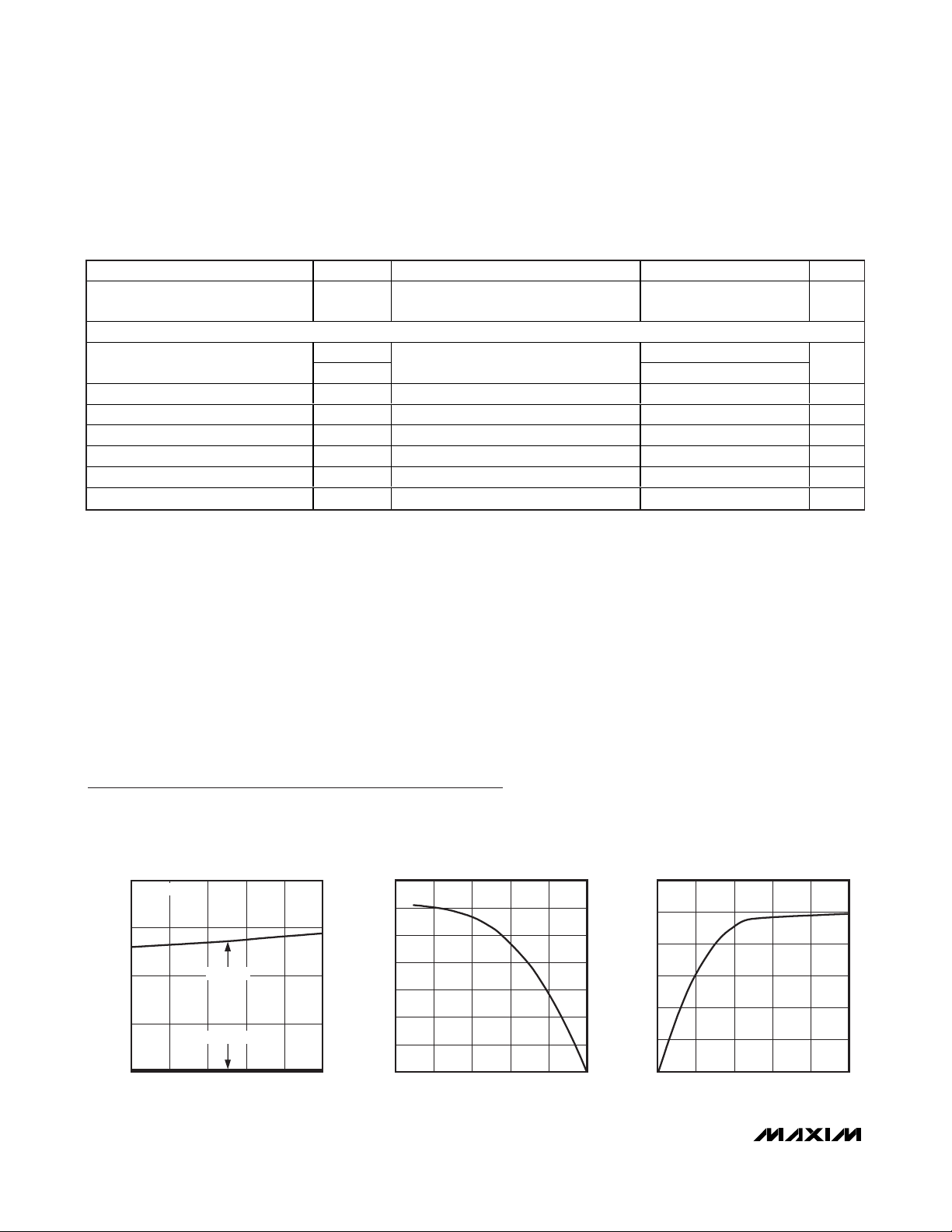
Typical Operating Characteristics
(VCC= +7.5V, TA= +25°C, unless otherwise noted.)
PARAMETER SYMBOL CONDITIONS MIN TYP MAX UNITS
Driver Disable from Output Low t
RECEIVER
Receiver Propagation Delay
Receiver Output Skew t
Maximum Data Rate f
Receiver Enable to Output High t
Receiver Enable to Output Low t
Receiver Disable Time from Low t
Receiver Disable Time from High t
DLZ
t
RPLH
t
RPHL
RSKEW
MAX
RZH
RZL
RLZ
RZH
S1 closed, Figure 4,
= 500Ω, CL = 15pF
R
L
CL = 15pF (at RO), Figures 5 and 6
CL = 15pF (at RO), Figures 5 and 6 8 ns
16 Mbps
S2 closed, Figure 7, CL = 15pF 50 ns
S1 closed, Figure 7, CL = 15pF 50 ns
S1 closed, Figure 7, CL = 15pF 50 ns
S2 closed, Figure 7, CL = 15pF 50 ns
50 ns
75
75
ns
SUPPLY CURRENT
vs. TEMPERATURE
8.0
NO LOAD
6.0
4.0
SUPPLY CURRENT (mA)
2.0
DE = HIGH
DE = LOW
MAX13410E-15E toc01
OUTPUT CURRENT (mA)
vs. RECEIVER OUTPUT HIGH VOLTAGE
35
30
25
20
15
10
5
OUTPUT CURRENT
OUTPUT CURRENT
60
50
MAX13410E-15E toc02
40
30
20
OUTPUT CURRENT (mA)
10
vs. RECEIVER OUTPUT LOW VOLTAGE
MAX13410E-15E toc03
0
-40 10-15 35 60 85
TEMPERATURE (°C)
0
021345
OUTPUT HIGH VOLTAGE (V)
0
05
OUTPUT LOW VOLTAGE (V)
2134
Page 9

MAX13410E–MAX13415E
RS-485 Transceiver with Integrated Low-Dropout
Regulator and AutoDirection Control
_______________________________________________________________________________________
9
Typical Operating Characteristics (continued)
(VCC= +7.5V, TA= +25°C, unless otherwise noted.)
RECEIVER OUTPUT HIGH VOLTAGE
IO = +1mA
R
= 54Ω
DIFF
vs. TEMPERATURE
MAX13410E-15E toc04
OUTPUT LOW VOLTAGE (V)
TEMPERATURE (°C)
vs. TEMPERATURE
120
100
MAX13410E-15E toc07
OUTPUT CURRENT (mA)
TEMPERATURE (°C)
5.4
5.2
5.0
4.8
4.6
4.4
OUTPUT HIGH VOLTAGE (V)
4.2
4.0
-40 10-15 35 60 85
DRIVER DIFFERENTIAL OUTPUT VOLTAGE
4.0
3.5
3.0
2.5
2.0
1.5
1.0
DIFFERENTIAL OUTPUT VOLTAGE (V)
0.5
0
-40 10-15 35 60 85
RECEIVER OUTPUT LOW VOLTAGE
vs. TEMPERATURE
0.5
IO = -1mA
0.4
0.3
0.2
0.1
0
-40 10-15 35 60 85
TEMPERATURE (°C)
OUTPUT CURRENT
vs. TRANSMITTER OUTPUT HIGH VOLTAGE
80
60
40
20
0
-7 -5 -4 -3-6 -2 0-1 12345
OUTPUT HIGH VOLTAGE (V)
80
60
MAX13410E-15E toc05
40
OUTPUT CURRENT (mA)
20
120
100
MAX13410E-15E toc08
80
60
40
OUTPUT CURRENT (mA)
20
DIFFERENTIAL OUTPUT CURRENT
vs. DIFFERENTIAL OUTPUT VOLTAGE
0
021 345
OUTPUT VOLTAGE (V)
OUTPUT CURRENT
vs. TRANSMITTER OUTPUT LOW VOLTAGE
0
0462 8 10 12
OUTPUT LOW VOLTAGE (V)
MAX13410E-15E toc06
MAX13410E-15E toc09
SHUTDOWN CURRENT
vs. TEMPERATURE
100
90
80
70
60
50
40
30
SHUTDOWN CURRENT (μA)
20
10
0
-40 10-15 35 60 85
TEMPERATURE (°C)
DRIVER PROPAGATION vs. TEMPERATURE
700
RL = 110Ω
600
MAX13410E-15E toc10
500
400
300
200
DRIVER PROPAGATION DELAY (ns)
100
0
-40 10-15 35 60 85
(MAX13412E)
t
RPLH
t
RPHL
TEMPERATURE (°C)
DRIVER PROPAGATION vs. TEMPERATURE
40
RL = 110Ω
35
30
MAX13410E-15E toc11
25
20
15
10
DRIVER PROPAGATION DELAY (ns)
5
0
-40 10-15 35 60 85
(MAX13413E)
t
RPHL
t
RPLH
TEMPERATURE (°C)
MAX13410E-15E toc12
Page 10

MAX13410E–MAX13415E
RS-485 Transceiver with Integrated Low-Dropout
Regulator and AutoDirection Control
10 ______________________________________________________________________________________
Typical Operating Characteristics (continued)
(VCC= +7.5V, TA= +25°C, unless otherwise noted.)
RECEIVER PROPAGATION vs.TEMPERATURE
(MAX13410E/MAX13412E)
60
t
45
30
15
RECEIVER PROPAGATION DELAY (ns)
0
-40 10-15 35 60 85
RPHL
t
RPLH
TEMPERATURE (°C)
MAX13410E-15E toc13
DRIVER PROPAGATION (16kbps)
(MAX13413E)
MAX13410E-15E toc16
DI
2V/div
A - B
5V/div
RECEIVER PROPAGATION vs.TEMPERATURE
(MAX13411E/MAX13413E)
60
45
30
15
RECEIVER PROPAGATION DELAY (ns)
0
-40 10-15 35 60 85
TEMPERATURE (°C)
RECEIVER PROPAGATION (16kbps)
(MAX13413E)
t
RPHL
t
RPLH
MAX13410E-15E toc17
MAX13410E-15E toc14
A
2V/div
B
2V/div
RO
2V/div
DRIVER PROPAGATION (250kbps)
(MAX13412E)
1μs/div
MAX13410E-15E toc15
DRIVING A LARGE CAPACITIVE LOAD 16nF
(19.2kbps) (MAX13412E)
MAX13410E-15E toc18
DI
2V/div
A - B
5V/div
DI
2V/div
A - B
2V/div
20ns/div
DRIVING A LARGE CAPACITIVE LOAD 16nF
(1Mbps) (MAX13413E)
400ns/div
MAX13410E-15E toc19
DI
2V/div
A - B
5V/div
20ns/div
DRIVING A LARGE CAPACITIVE LOAD 16nF
(50kbps) (MAX13413E)
1μs/div
MAX13410E-15E toc20
10μs/div
DI
2V/div
A - B
2V/div
Page 11

MAX13410E–MAX13415E
RS-485 Transceiver with Integrated Low-Dropout
Regulator and AutoDirection Control
______________________________________________________________________________________ 11
Figure 1. Driver DC Test Load
Figure 3a. Driver Propagation Delays
Test Circuits and Waveforms
Figure 2a. Driver-Timing Test Circuit
Figure 2b. Driver-Timing Test Circuit
A
V
OD
B
5V
DE
A
DI
B
/ 2
R
DIFF
C
L
V
R
/ 2
OC
DIFF
R
L
A
V
ID
R
DIFF
C
L
DI
V
ID
B
V
REG
GND
R
C
L
L
5V
DI
0
B
A
1/2 V
V
O
V
O
V
0
DIFF
-V
O
LH
10%
f = 1MHz, tLH ≤ 3ns, tHL ≤ 3ns
B
DPHL
1.5V
1/2 V
t
DPHL
90%
t
HLt
|
O
10%
1.5V
t
DPLH
O
= VA - V
V
DIFF
90%
t
= |t
DPLH
- t
DSKEW
Page 12

MAX13410E–MAX13415E
RS-485 Transceiver with Integrated Low-Dropout
Regulator and AutoDirection Control
12 ______________________________________________________________________________________
Test Circuits and Waveforms (continued)
Figure 3b. Driver Propagation Delays
Figure 4. Driver Enable and Disable Times
Figure 5. Receiver-Propagation-Delay Test Circuit
f = 1MHz, tLH ≤ 3ns, tHL ≤ 3ns
RE = V
5V
DI
0
B
V
O
A
1/2 V
1.5V
O
CC
t
DPLH
t
DPHL
1.5V
1/2 V
O
RO
O
V
O
V
DIFF
0
-V
O
OUTPUT
UNDER TEST
500Ω
C
L
(RO PULLED LOW)
10%
t
LH
5V
S
1
S
2
t
, t
DDD
RED
90%
V
CC
DE
0
A, B
V
OL
A, B
0
V
DIFF
= VA - V
1.5V
2.3V
2.3V
B
t
DZL(SHDN)
t
DZH(SHDN)
90%
t
HL
OUTPUT NORMALLY LOW
OUTPUT NORMALLY HIGH
10%
1.5V
t
DLZ
V
+ 0.5V
OL
V
OH
+ 0.5V
V
OH
t
DHZ
B
RECEIVER
ATE
V
ID
R
OUTPUT
A
Page 13

MAX13410E–MAX13415E
RS-485 Transceiver with Integrated Low-Dropout
Regulator and AutoDirection Control
______________________________________________________________________________________ 13
Test Circuits and Waveforms (continued)
Figure 6. Receiver Propagation Delays
Figure 7. Receiver Enable and Disable Times
A
B
V
OH
RO
V
OL
C
L
15pF
1kΩ
RO
S
1
S
2
f = 1MHz, t
t
RPHL
1.5V
V
REG
RE
0
V
REG
RO
5V
0
V
REG
RO
0
DI = 0V
≤ 3ns, tHL ≤ 3ns
LH
t
= | t
RSKEW
RPHL
1.5V
t
RZL(SHDN)
2.3V
2.3V
t
RZH(SHDN)
1V
-1V
t
RPLH
1.5V
- t
RPLH |
1.5V
, t
RZL
OUTPUT NORMALLY LOW
OUTPUT NORMALLY HIGH
, t
t
RZH
t
RHZ
+ 0.5V
V
OH
+ 0.5V
V
OH
RHZ
Page 14

MAX13410E–MAX13415E
RS-485 Transceiver with Integrated Low-Dropout
Regulator and AutoDirection Control
14 ______________________________________________________________________________________
Pin Description
PIN
MAX13410E/
MAX13411E
NAME FUNCTION
1—1RO
Receiver Output. When receiver is enabled and V
A
- VB ≥ -50mV,
RO is high. If V
A
- VB ≤ -200mV, RO is low. Note: RO is referenced to
the LDO output (V
REG
).
2——RE
Receiver Output Enable. Drive RE low to enable RO. Drive RE high to
disable the RO output and put the RO output in a high-impedance
state.
3——DE
D r i ver Outp ut E nab l e. D r i ve D E l ow to p ut the d r i ver outp ut i n thr ee- state.
D r i ve D E hi g h to enab l e the d r i ver .
444DI
Driver Input. Drive DI low to force the noninverting output low and the
inverting output high. Drive DI high to force the noninverting output
high and inverting output low. DI is an input to the internal state
machine that automatically enables and disables the driver (for the
MAX13412E/MAX13413E). See the function tables and General
Description for more information.
5 5 5 GND Ground
6 6 6 A Noninverting Receiver Input and Noninverting Driver Output
7 7 7 B Inverting Receiver Input and Inverting Driver Output
888V
CC
Positive Supply. Bypass VCC with a 0.1µF ceramic capacitor to GND.
—1—RO
Receiver Output. When receiver is enabled and V
A
- VB ≥ -100mV,
RO is high. If V
A
- VB ≤ -100mV, RO is low. Note: RO is referenced to
the LDO output (V
REG
).
—2—RE
Receiver Output Enable. Drive RE low to force the RO output to be
enabled. Drive RE high to let the AutoDirection circuit control RO.
—3 3V
REG
LDO Output. V
REG
is fixed at +5V. Bypass V
REG
with a low ESR
(20mΩ or less) and a 1µF (min) ceramic capacitor.
— — 2 DE/RE
Receiver and Driver Output Enable. Drive DE/RE low to enable RO
and disable the driver. Drive DE/RE high to disable RO and enable
the driver.
EP EP EP EP
Exposed Pad. EP is internally connected to GND. For enhanced
thermal dissipation, connect EP to a copper area as large as
possible. Do not use EP as a sole ground connection.
MAX13412E/
MAX13413E
MAX13414E/
MAX13415E
Page 15

MAX13410E–MAX13415E
RS-485 Transceiver with Integrated Low-Dropout
Regulator and AutoDirection Control
______________________________________________________________________________________ 15
Function Tables for the MAX13410E/MAX13411E
X
= Don’t care, shutdown mode, driver, and receiver outputs are in high impedance.
Function Tables for the MAX13414E/MAX13415E
X
= Don’t care, shutdown mode, driver, and receiver outputs are in high impedance.
Function Tables for the MAX13412E/MAX13413E
X
= Don’t care, shutdown mode, driver, and receiver outputs are in high impedance.
TRANSMITTING
INPUT OUTPUT
RE DE DI B A
X11 0 1
X10 1 0
0 0 X High impedance High impedance
1 0 X High impedance (shutdown)
RE DE A - B RO
0X > -50mV 1
0X < -200mV 0
0 X Open/Short 1
1 1 X High impedance
10 X
INPUT OUTPUT
RECEIVING
TRANSMITTING
INPUTS OUTPUTS
DI A - B > V
0 X Turn driver ON 0 1
1 False If driver was OFF, keep it OFF High impedance High impedance
1 False If driver was ON, keep it ON 1 0
1 True Turn driver OFF High impedance High impedance
DT
ACTION A B
High impedance
(shutdown)
RECEIVING
INPUTS OUTPUT
RE A - B DRIVER STATE RECEIVER STATE RO
0 > -100mV X ON 1
0 < -100mV X ON 0
1 X ON OFF High impedance
1 > -100mV OFF ON 1
1 < -100mV OFF ON 0
TRANSMITTING
INPUT OUTPUT
DE/RE DI B A
0 X High impedance High impedance
11 0 1
10 1 0
DE/RE A - B RO
INPUT OUTPUT
0 > -50mV 1
0 < -200mV 0
0 Open/Short 1
1 X High impedance
RECEIVING
Page 16

MAX13410E–MAX13415E
Detailed Description
The MAX13410E–MAX13415E are half-duplex RS-485/
RS-422-compatible transceivers optimized for isolated
applications. These devices feature an internal LDO regulator, one driver, and one receiver. The internal LDO
allows the part to operate from an unregulated +6V to
+28V power supply. The AutoDirection feature reduces
the number of optical isolators needed in isolated applications. Other features include ±15kV ESD protection
(MAX13412E/MAX13413E only), ±14kV (MAX13410E/
MAX13411E only) fail-safe circuitry, slew-rate limiting, and
full-speed operation.
The MAX13410E–MAX13415E internal LDO generates a
5V ±10% power supply that is used to power its internal
circuitry. The MAX13412E–MAX13415E bring the 5V to an
output V
REG
that allows the user to power additional external circuitry with up to 20mA to further reduce external
components. The MAX13410E/MAX13411E do not have a
5V output and come in industry-compatible pinouts. This
allows easy replacement in existing designs.
The MAX13412E/MAX13413E feature Maxim’s proprietary AutoDirection control. This architecture eliminates
the need for the DE and RE control signals. In isolated
applications, this reduces the cost and size of the system by reducing the number of optical isolators required.
The MAX13410E/MAX13412E/MAX13414E feature
reduced slew-rate drivers that minimize EMI and reduce
reflections caused by improperly terminated cables,
allowing error-free transmission up to 500kbps. The
MAX13411E/MAX13413E/MAX13415E are not slew-rate
limited, allowing transmit speeds up to 16Mbps.
The MAX13410E–MAX13415E feature a 1/8-unit load
receiver input impedance, allowing up to 256 transceivers on the bus. All driver outputs are protected to
±15kV ESD using the Human Body Model. These
devices also include fail-safe circuitry, MAX13410E/
MAX13411E/MAX13414E/MAX13415E, guaranteeing a
logic-high receiver output when the receiver inputs are
open or shorted. The receiver outputs a logic-high
when the transmitter on the terminated bus is disabled
(high impedance).
Internal Low-Dropout Regulator
The MAX13410E–MAX13415E include an internal lowdropout regulator that allows it to operate from input voltages of up to +28V. The internal LDO has a set output
voltage of 5V ±10% that is used to power the internal circuitry of the device. The MAX13412E–MAX13415E offer
the LDO output at the V
REG
output. This allows additional
external circuitry to be powered without the need for
additional external regulators. The V
REG
output can
source up to 20mA.
When using these devices with high input voltages and
heavily loaded networks, special care must be taken
that the power dissipation rating of the package and
the maximum die temperature of the device is not
exceeded. Die temperature of the part can be calculated using the equation:
T
DIE
= [(
θ
JC
+
θ
CA
) x P
DISS
] + T
AMBIENT
, where
T
DIE
= Temperature of the Die
θ
JC
= 6.0°C/W = Junction-to-Case Thermal Resist-
ance
θ
CA
= Case-to-Ambient Thermal Resistance
θ
JA
=
θ
JC
+
θ
CA
= 52.0°C/W = Junction-to-Ambient
Thermal Resistance
P
DISS
= (ICC- VCC) + [(VCC- V
REG
) x I
REG
)] + [(VCC-
VOD) x I
DRIVER
] = Power Dissipation of the Part
T
AMBIENT
= Ambient Temperature
VCC= Voltage on the VCCInput
ICC= Current in to V
CC
V
REG
= Voltage on the V
REG
Output
I
REG
= Current Drawn from the V
REG
Output
VOD= Voltage at the Driver Output (|VA- VB|)
I
DRIVER
= Current Driven Out of the Driver. Typically,
this is the current through the termination resistor.
The absolute maximum rating of the die temperature of
the MAX13410E–MAX13415E is +150°C. To protect the
part from overheating, there is an internal thermal shutdown that shuts down the part when the die temperature reaches +150°C. To prevent damage to the part,
and to prevent the part from entering thermal shutdown,
keep the die temperature below +150°C, plus some
margin. The circuit designer can minimize the die temperature by controlling the following parameters:
•V
CC
•I
REG
•
θ
CA
Measuring the VCCCurrent
Measured current at the VCCpin is a function of the
quiescent current of the part, the amount of current that
the drivers must supply to the load, and in the case of
the MAX13412E–MAX13415E, the load on the V
REG
output. In most cases, the load that the drivers must
supply will be the termination resistor(s). Ideally, the termination resistance should match the characteristic
impedance of the cable and is usually not a parameter
the circuit designer can easily change. In some lowspeed, short-cable applications, proper termination
RS-485 Transceiver with Integrated Low-Dropout
Regulator and AutoDirection Control
16 ______________________________________________________________________________________
Page 17

may not be necessary. In these cases, the drive current
can be reduced to minimize the die temperature.
Minimizing the load on the V
REG
output lowers the
power dissipation of the part and ultimately reduces the
maximum die temperature.
θθ
CA
θ
CA
is the thermal resistance from case to ambient and
is independent of the MAX13410E–MAX13415E.
θ
CA
is
primarily a characteristic of the circuit-board design. The
largest contributing factor of
θ
CA
will be the size and
weight of the copper connected to the exposed paddle
of the MAX13410E–MAX13415E. Lower the thermal
resistance by using as large a pad as possible.
Additionally, vias can be used to connect the pad to
other ground planes in the circuit board.
Note that
θ
JC
is the thermal resistance of the part from
junction-to-case temperature and is fixed at 6.0°C/W. It is
solely based on the die and package characteristics of
MAX13410E–MAX13415E
RS-485 Transceiver with Integrated Low-Dropout
Regulator and AutoDirection Control
______________________________________________________________________________________ 17
Functional Diagrams
Functional Diagram for the MAX13410E/MAX13411E/MAX13414E/MAX13415E
Functional Diagram for the MAX13412E/MAX13413E
DERO3
1
2
4
MAX13410E
MAX13411E
+
R
1
RO
2
LDO
87V
CC
BRE
6
A
D
5
GNDDI
RO
V
REG
V
MAX13412E
MAX13413E
RE
REG
V
REG
R
RE
1
2
3
4
+
-
+
LDO
MAX13414E
MAX13415E
R
D
LDO
87V
CC
BDE/RE
6
A
5
GNDDI
V
8
CC
3
V
REG
STATE
RI
MACHINE
DI
4
DI
7
GND
B
6
A
5
-
V
COM
DT
+
DE
V
REG
D
Page 18

MAX13410E–MAX13415E
the MAX13410E–MAX13415E. The circuit-board designer
has no control over this parameter.
Fail Safe
The MAX13410E/MAX13411E/MAX13414E/MAX13415E
guarantee a logic-high receiver output when the receiver inputs are shorted or open, or when they are connected to a terminated transmission line with all drivers
disabled. This is done by setting the receiver input
threshold between -50mV and -200mV. If the differential
receiver input voltage (A - B) is greater than or equal to
-50mV, RO is logic-high. If (A - B) is less than or equal
to -200mV, RO is logic-low. In the case of a terminated
bus with all transmitters disabled, the receiver’s differential input voltage is pulled to 0 by the termination.
With the receiver thresholds of the MAX13410E/
MAX13411E/MAX13414E/MAX13415E, the result is a
logic-high with a 50mV minimum noise margin. Unlike
previous fail-safe devices, the -50mV to -200mV threshold complies with the ±200mV EIA/TIA-485 standard.
AutoDirection Circuitry
The AutoDirection circuitry in the MAX13412E/
MAX13413E is a technique to minimize the number of
signals needed to drive the part. This is especially useful
in very low cost, isolated systems. In a typical isolated
system, an optocoupler is used for each control signal to
cross the isolation barrier. These optocouplers add cost,
size and consume power. Without the AutoDirection circuitry, three to four optocouplers may be required for
each transceiver. With the AutoDirection circuitry, the
number of optocouplers can be reduced to two.
Typical RS-485 transceivers have four signals on the
control side of the part. These are RO (receiver output),
RE (receiver enable), DE (driver enable), and DI (driver
input). In some cases, DE and RE may be connected
together to reduce the number of control signals to
three. In half-duplex systems, the RE and DE signals
determine if the part is transmitting or receiving. When
the part is receiving, the transmitter is in a high-impedance state. In a fully compliant RS-485 system, all three
or four signals are required. However, with careful
design and Maxim’s AutoDirection feature, the number
of control signals can be reduced to just RO and DI in
an RS-485 compatible system. This feature assumes the
DI input idles in the high state while the receiver portion
of the MAX13412E/MAX13413E is active. It also requires
an external pullup resistor on A and pulldown resistor on
B (see the typical application circuit, Figure 10). The following is a description of how AutoDirection works.
When DI is low, the MAX13412E/MAX13413E always
drive the bus low. When DI transitions from a low to a
high, the drivers actively drive the output until (A - B) >
VDT. Once (A - B) is greater than VDT, the drivers are
disabled, letting the pullup/pulldown resistors hold the
A and B lines in the correct state. This allows other
transmitters on the bus to pull the bus low.
Pullup and Pulldown Resistors
The pullup and pulldown resistors on the A and B lines
are required for proper operation of the MAX13412E
and MAX13413E, although their exact value is not critical. They function to hold the bus in the high state (A - B
> 200mV) when all the transmitters are in a high-impedance state due to either a shutdown condition or
AutoDirection. Determining the best value to use for
these resistors depends on many factors, such as termination resistor values, noise, number of transceivers on
the bus, etc. Size these resistors so that, under all conditions, (A - B) > 200mV for ALL receivers on the bus.
Idle State
When not transmitting data, the MAX13412E/
MAX13413E require the DI input to be driven high to
remain in the idle state. A conventional RS-485 transceiver has DE and RE inputs that are used to enable
and disable the driver and receiver. However, the
MAX13412E/MAX13413E do not have a DE input, and
instead use an internal state machine to enable and
disable the drivers. DI must be driven high to go to the
idle state.
Enhanced ESD Protection
As with all Maxim devices, ESD-protection structures are
incorporated on all pins to protect against electrostatic
discharges encountered during handling and assembly.
The driver outputs and receiver inputs of the MAX13410E–
MAX13415E have extra protection against static electricity.
Maxim’s engineers have developed state-of-the-art structures to protect these pins against ESD of ±15kV
(MAX13412E/MAX13413E) and ±14kV (MAX13410E/
MAX13411E) without damage. The ESD structures withstand high ESD in all states: normal operation, shutdown,
and powered down. After an ESD event, the MAX13410E–
MAX13415E keep working without latchup or damage.
ESD protection can be tested in various ways. The transmitter outputs and receiver inputs of the MAX13410E–
MAX13415E are characterized for protection to the
following limits:
±15kV using the Human Body Model (MAX13412E/
MAX13413E)
±14kV using the Human Body Model (MAX13410E/
MAX13411E)
RS-485 Transceiver with Integrated Low-Dropout
Regulator and AutoDirection Control
18 ______________________________________________________________________________________
Page 19

ESD Test Conditions
ESD performance depends on a variety of conditions.
Contact Maxim for a reliability report that documents
test setup, test methodology, and test results.
Human Body Model
Figure 8a shows the Human Body Model, and Figure
8b shows the current waveform it generates when discharged into a low impedance. This model consists of
a 100pF capacitor charged to the ESD voltage of interest, which is then discharged into the test device
through a 1.5kΩ resistor.
Applications Information
Typical Applications
The MAX13410E–MAX13415E transceivers are designed
for half-duplex, bidirectional data communications on
multipoint bus transmission lines. To minimize reflections,
terminate the line at both ends in its characteristic
impedance, and keep stub lengths off the main line as
short as possible. The slew-rate-limited MAX13410E/
MAX13412E/MAX13414E are more tolerant of imperfect
termination.
Typical Application Circuit for the
MAX13410E and MAX13411E
This application circuit shows the MAX13410E/
MAX13411E being used in an isolated application (see
Figure 9). The MAX13410E/MAX13411E use the industrystandard pin out but do not have a V
REG
output for
biasing external circuitry. The positive temperature coefficient (PTC) and transient voltage suppressor (TVS)
clamp circuit on the RS-485 outputs are intended to provide overvoltage fault protection and are optional based
on the requirements of the design.
Typical Application Circuit for the
MAX13412E and MAX13413E
This application circuit shows the MAX13412E and
MAX13413E being used in an isolated application
where the AutoDirection feature is implemented to
reduce the number of optical isolators to two (see
Figure 10). The MAX13412E/MAX13413E provide a
V
REG
output that can be used to power external circuit-
ry up to 20mA.
Typical Application Circuit for the
MAX13414E and MAX13415E
This application circuit shows the MAX13414E/
MAX13415E being used in an isolated application using
an unregulated power supply with three optical isolators
(see Figure 11). The MAX13414E/MAX13415E provide a
V
REG
output that can be used to power external circuitry
up to 20mA.
256 Transceivers on the Bus
The RS-485 standard specifies the load each receiver
places on the bus in terms of unit loads. An RS-485compliant transmitter can drive 32 one-unit load
receivers when used with a 120Ω cable that is terminated on both ends over a -7V to +12V common-mode
range. The MAX13410E–MAX13415E are specified as
1/8 unit loads. This means a compliant transmitter can
drive up to 256 devices of the MAX13410E–MAX13415E.
Reducing the common mode, and/or changing the characteristic impedance of the cable, changes the maximum number of receivers that can be used. Refer to the
TIA/EIA-485 specification for further details.
Proper Termination and Cabling/
Wiring Configurations
When the data rates for RS-485 are high relative to the
cable length it is driving, the system is subject to proper
MAX13410E–MAX13415E
RS-485 Transceiver with Integrated Low-Dropout
Regulator and AutoDirection Control
______________________________________________________________________________________ 19
Figure 8a. Human Body ESD Test Model
Figure 8b. Human Body Current Waveform
R
C
1MΩ
CHARGE-CURRENT-
LIMIT RESISTOR
HIGH-
VOLTAGE
DC
SOURCE
100pF
C
s
R
D
1500Ω
DISCHARGE
RESISTANCE
STORAGE
CAPACITOR
DEVICE
UNDER
TEST
IP 100%
90%
AMPS
36.8%
10%
0
0
t
RL
TIME
CURRENT WAVEFORM
I
r
t
DL
PEAK-TO-PEAK RINGING
(NOT DRAWN TO SCALE)
Page 20

MAX13410E–MAX13415E
transmission line design. In most cases, a single, controlled-impedance cable or trace should be used and
should be properly terminated on both ends with the
characteristic impedance of the cable/trace. RS-485
transceivers should be connected to the cable/ traces
with minimum-length wires to prevent stubs. Star configurations and improperly terminated cables can cause
data loss. Refer to the
Application Notes
section of the
Maxim website or to TIA/EIA publication TSB-89-A for
further information. While proper termination is always
desirable, in some cases, such as when data rates are
very low, it may be desirable and advantageous to not
properly terminate the cables. In such cases, it is up to
the designer to ensure that the improper termination
and resultant reflections (etc.) will not corrupt the data.
Reduced EMI and Reflections
The MAX13410E/MAX13412E/MAX13414E feature
reduced slew-rate drivers that minimize EMI and reduce
reflections caused by improperly terminated cables,
allowing error-free data transmission up to 500kbps.
Low-Power Shutdown Mode
Low-power shutdown mode is initiated in the
MAX13410E/MAX13411E by driving DE low and driving
RE high. In shutdown, the devices draw 65µA (typ) of
supply current.
The devices are guaranteed not to enter shutdown if
DE is low (while RE is high) for less than 50ns. If the
inputs are in this state for at least 700ns, the devices
are guaranteed to enter shutdown.
Enable times t
ZH
and tZL(see the switching characteristics table) assume the devices were not in a low-power
shutdown state. Enable times t
ZH(SHDN)
and t
ZL(SHDN)
assume the devices were in shutdown state. It takes drivers and receivers longer to become enabled from lowpower shutdown mode (t
ZH(SHDN)
, t
ZL(SHDN)
) than from
driver/receiver disable mode (tZH, tZL).
Line Length
The Telecommunications Industry Association (TIA) published the document TSB-89-A:
Application Guidelines
for TIA/EIA-485-A
, which is a good reference for deter-
mining maximum data rate vs. line length.
Isolated RS-485 Interface
An isolated RS-485 interface electrically isolates different
nodes on the bus to protect the bus from problems due
to high common-mode voltages that exceed the RS-485
common-mode voltage range, conductive noise, and
RS-485 Transceiver with Integrated Low-Dropout
Regulator and AutoDirection Control
20 ______________________________________________________________________________________
Figure 9. Typical Application Circuit for the MAX13410E/MAX13411E
R
t
UNREGULATED ISOLATED
+
RO
1
RE
2
POWER SUPPLY
R
LDO
ISO_V
V
CC
8
B
7
CC
0.1μF
V
SYS
MCU AND
RELATED
CIRCUITRY
ISO_V
ISO_V
CC
N
CC
ISO_V
CC
DE
3
DI
4
D
MAX13410E
MAX13411E
A
6
GND
5
R
t
Page 21

ground loops. The typical application circuits show an
isolated RS-485 interface using the MAX13410E–
MAX13415E. The transceiver is powered separately from
the controlling circuitry. The AutoDirection feature of the
MAX13412E/MAX13413E (see the
AutoDirection Circuitry
section) requires only two optocouplers to electrically
isolate the transceiver.
An isolated RS-485 interface electrically isolates different nodes on the bus to protect the bus from problems
due to high common-mode voltages that exceed the
RS-485 common-mode voltage range. An isolated RS485 interface has two additional design challenges not
normally associated with RS-485 design. These are 1)
isolating the control signals and 2) getting isolated
power to the transceiver. Optical isolators are the most
common way of getting the control signals across the
isolation barrier.
Isolated power is typically done using a transformer in
either a push-pull or flyback configuration. The MAX845
is an example of an inexpensive, unregulated push-pull
converter (see Figure 12). While in theory, the output of
an unregulated push-pull converter is predictable, the
output voltage can vary significantly due to the non-ideal
characteristics of the transformer, load variations, and
temperature drift of the diodes, etc. Variances of ±20%
or more would not be uncommon. This would require the
addition of a linear regulator to get standard RS-485
transceivers to work. Since the MAX13410E–
MAX13415E have the linear regulator built in, this external regulator and its associated cost and size penalties
are not necessary. A nominal +7.5V output with a ±20%
tolerance would provide a +6V to +9V supply voltage.
This is well within the operating range of the
MAX13410E–MAX13415E. If the output tolerance is even
greater than ±20%, adjust the design of the power supply for a higher output voltage to ensure the minimum
input voltage requirements are met.
Flyback converters are typically regulated. A TL431 type
error amplifier and an optical isolator usually close the
loop. The MAX5021 is an example of a small, inexpensive, flyback controller (see Figure 13). While the primary output of the flyback converter is tightly regulated,
secondary outputs will not be. As with the unregulated
push-pull converter, the MAX13410E–MAX13415E are
ideally suited for use with these secondary outputs.
MAX13410E–MAX13415E
RS-485 Transceiver with Integrated Low-Dropout
Regulator and AutoDirection Control
Figure 10. Typical Application Circuit for the MAX13412E/MAX13413E
______________________________________________________________________________________ 21
ISO_V
MCU AND
RELATED
CIRCUITRY
CC
V
SYS
ISO_V
CC
ISO_V
CC
ISO_V
CC
C
1μF
V
SYS
S
RO
1
RE
2
V
REG
3
DI
4
UNREGULATED ISOLATED
+
DETECT
CIRCUIT
POWER SUPPLY
R
D
MAX13412E
MAX13413E
LDO
R
t
V
CC
8
7
6
5
B
A
GND
0.1μF
ISO_V
CC
R
t
Page 22

MAX13410E–MAX13415E
RS-485 Transceiver with Integrated Low-Dropout
Regulator and AutoDirection Control
22 ______________________________________________________________________________________
Figure 11. Typical Application Circuit for the MAX13414E/MAX13415E
Figure 12. Using the MAX845 to Obtain an Isolated Power Supply
Figure 13. The MAX5021 and MAX5022 provide an isolated
power supply with tighter regulation due to feedback using an
opto-isolator coupler.
R
t
ISO_V
MCU AND
RELATED
CIRCUITRY
CC
V
SYS
ISO_V
CC
V
SYS
ISO_V
CC
V
SYS
ISO_V
C
S
DE/RE
CC
RO
1
2
V
REG
3
1μF
DI
4
UNREGULATED ISOLATED
POWER SUPPLY
+
R
D
LDO
MAX13414E
MAX13415E
V
CC
8
7
6
5
0.1μF
B
A
GND
V
5V
ON / OFF
46
SD
MAX845
3
FREQUENCY
SELECT
GND1 GND2
27
IN
C1
V
CC
1
D1
8
D2FS
CR1
T1
CR2
OUTPUT
5V AT 150mA
C2
C3
R
t
V
SUPPLY
V
OUT
V
IN
V
CC
MAX5021/
MAX5022
OPTO NDRV
CS
GND
Page 23

MAX13410E–MAX13415E
RS-485 Transceiver with Integrated Low-Dropout
Regulator and AutoDirection Control
______________________________________________________________________________________ 23
Ordering Information/Selector Guide (continued)
Note: All devices operate over the -40°C to +85°C operating
temperature range.
+
Denotes a lead(Pb)-free/RoHS-compliant package.
*
EP = Exposed pad.
**
Future product—contact factory for availability.
Pin Configurations (continued)
Chip Information
PROCESS TECHNOLOGY: BiCMOS
PACKAGE TYPE PACKAGE CODE DOCUMENT NO.
8 SO-EP S8E+14
21-0111
Package Information
For the latest package outline information and land patterns,
go to www.maxim-ic.com/packages
. Note that a “+”, “#”, or
“-” in the package code indicates RoHS status only. Package
drawings may show a different suffix character, but the drawing
pertains to the package regardless of RoHS status.
TOP VIEW
*EXPOSED PAD CONNECTED TO GROUND
+
1
RO
2
MAX13412E
3
V
REG
MAX13413E
4
SO
*EP
87V
6
5
CC
BRE
A
GNDDI
V
REG
+
1
RO
2
MAX13414E
3
MAX13415E
4
SO
*EP
87V
6
5
CC
BDE/RE
A
GNDDI
PART PIN-PACKAGE AutoDirection DATA RATE (max) 5V LDO OUTPUT
MAX13412EESA+ 8 SO-EP* Yes 500kbps Yes
MAX13413EESA+ 8 SO-EP* Yes 16Mbps Yes
MAX13414EESA+** 8 SO-EP* No 500 kbps Yes
MAX13415EESA+** 8 SO-EP* No 16Mbps Yes
Page 24

MAX13410E–MAX13415E
RS-485 Transceiver with Integrated Low-Dropout
Regulator and AutoDirection Control
Maxim cannot assume responsibility for use of any circuitry other than circuitry entirely embodied in a Maxim product. No circuit patent licenses are
implied. Maxim reserves the right to change the circuitry and specifications without notice at any time.
24
____________________Maxim Integrated Products, 120 San Gabriel Drive, Sunnyvale, CA 94086 408-737-7600
© 2009 Maxim Integrated Products Maxim is a registered trademark of Maxim Integrated Products, Inc.
Revision History
REVISION
NUMBER
0 11/07 Initial release. —
1 8/09 Replaced Figure 9. 20
REVISION
DATE
DESCRIPTION
PAGES
CHANGED
 Loading...