

Page 1
General Description
The MAX13041 ±80V fault-protected, high-speed controller area network (CAN) transceiver is ideal for highspeed automotive network applications where high
reliability and advanced power management are
required. The device links a CAN protocol controller to
the physical bus wires of the controller area network
and allows communication at speeds up to 1Mbps.
The extended fault-protected voltage range of ±80V on
CAN bus lines allows for use in +12V or +42V automotive, and higher voltage +24V and +36V mid-heavy truck
applications. Advanced power management features
make the MAX13041 ideal for automotive electronic control unit (ECU) modules that are permanently supplied by
battery, regardless of the ignition switch position (clamp30, Type-A modules). The device controls one or more
external voltage regulators to provide a low-power sleep
mode for an entire clamp-30 node. Wake-on CAN capability allows the MAX13041 to restore power to the node
upon detection of CAN bus activity.
The MAX13041 is functionally compatible with the
Philips TJA1041A and is a pin-to-pin replacement with
improved performance. The MAX13041 is available in a
14-pin SO package, and operates over the -40°C to
+125°C automotive temperature range.
Applications
+12V Automotive—Clamp 30 Modules
+42V Automotive—Clamp 30 Modules
+24V Mid-Heavy Truck—Clamp 30 Modules
Military and Commercial Aircraft
Features
♦ Functionally Compatible Pin-to-Pin Replacement
for the Philips TJA1041A
♦ ±12kV HBM ESD Protection on CANH, CANL
♦ ±80V Fault Protection on CANH, CANL, SPLIT;
Up to +76V Operation on V
BAT
♦ Fully Compatible with the ISO11898 Standard
♦ Low V
BAT
Supply Current in Standby and Sleep
Modes (18µA Typical)
♦ Voltage Level Translation for Interfacing with
+2.8V to +5.5V CAN Protocol Controllers
♦ Recessive Bus Stabilization (SPLIT)
♦ Allows Implementation of Large Networks
MAX13041
±80V Fault-Protected High-Speed CAN Transceiver
with Low-Power Management and Wake-On CAN
________________________________________________________________
Maxim Integrated Products
1
19-0747; Rev 1; 11/07
For pricing, delivery, and ordering information, please contact Maxim Direct at 1-888-629-4642,
or visit Maxim’s website at www.maxim-ic.com.
Ordering Information
V
I/O
V
CC
V
BAT
TXD
RXD
ERR
STB
CANH
CANL
EN
GND
INH
SPLIT
WAKE
BAT
C
SPLIT
60Ω
+3.3V
+5V
60Ω
+3.3V
CAN PROTOCOL
CONTROLLER
10kΩ
33kΩ
MAX13041
Typical Operating Circuit
+
Denotes a lead-free package.
Pin Configuration appears at end of data sheet.
PART
MAX13041ASD+
TEMP
RANGE
-40°C to
+125°C
PINPACKAGE
14 SOIC S14M-7
PKG
CODE
Page 2

MAX13041
±80V Fault-Protected High-Speed CAN Transceiver
with Low-Power Management and Wake-On CAN
2 _______________________________________________________________________________________
ABSOLUTE MAXIMUM RATINGS
Stresses beyond those listed under “Absolute Maximum Ratings” may cause permanent damage to the device. These are stress ratings only, and functional
operation of the device at these or any other conditions beyond those indicated in the operational sections of the specifications is not implied. Exposure to
absolute maximum rating conditions for extended periods may affect device reliability.
(All voltages referenced to GND.)
V
CC
, V
I/O
...................................................................-0.3V to +6V
V
BAT
........................................................................-0.3V to +80V
TXD, RXD, STB, EN, ERR .........................................-0.3V to +6V
INH, WAKE................................................-0.3V to (V
BAT
+ 0.3V)
CANH, CANL, SPLIT ................................0V to ±80V continuous
Continuous Power Dissipation (T
A
= +70°C)
14-Pin SO (derate 8.3mW/°C above +70°C).................667mW
Operating Temperature Range .........................-40°C to +125°C
Storage Temperature Range .............................-65°C to +150°C
Junction Temperature......................................................+150°C
Lead Temperature (soldering, 10s) .................................+300°C
ELECTRICAL CHARACTERISTICS
(VCC= +4.75V to +5.25V, V
I/O
= +2.8V to VCC, V
BAT
= +5V to +76V, TA= T
MIN
to T
MAX
, RL= 60Ω, unless otherwise noted. Typical
values are at V
CC
= +5V, V
I/O
= +3.3V, V
BAT
= +12V and TA= +25°C.) (Notes 1, 2)
)
)
)
)
PARAMETER SYMBOL CONDITIONS MIN TYP MAX UNITS
VCC Input Voltage V
V
Input Voltage V
I/O
Input Voltage V
V
BAT
VCC Undervoltage Detection
Level for Forced Sleep Mode
V
Undervoltage Detection
I/O
Level for Forced Sleep Mode
V
Voltage Level for Failsafe
BAT
Fallback Mode
V
Voltage Level for Setting
BAT
PWON Flag
VCC Input Current I
V
Input Current I
I/O
V
V
V
V
BAT(PWON
CC
I/O
BAT
CC(SLEEP
I/O(SLEEP
BAT(STBY
Operating range 4.75 5.25 V
Operating range 2.80 5.25 V
Operating range 5 76 V
VCC = +5V (fail-safe) 2.75 3.3 4.50 V
VCC = 0V 2.5 3.3 4.1 V
CC
Normal mode, V
Normal or PWON/listen-only mode,
V
= V
TXD
(recessive)
I/O
TXD
Standby or sleep mode 1.8 8 µA
I/O
Normal mode, V
Normal or PWON/listen-only mode,
= V
V
TXD
(recessive)
I/O
TXD
Standby or sleep mode, V
= 0V (dominant) 55 80
= 0V (dominant) 230 700
= V
TXD
I/O
2.75 3.3 4.50 V
0.5 1.5 2.0 V
610
15
0.7 3
mA
µA
Page 3

MAX13041
±80V Fault-Protected High-Speed CAN Transceiver
with Low-Power Management and Wake-On CAN
_______________________________________________________________________________________ 3
ELECTRICAL CHARACTERISTICS (continued)
(VCC= +4.75V to +5.25V, V
I/O
= +2.8V to VCC, V
BAT
= +5V to +76V, TA= T
MIN
to T
MAX
, RL= 60Ω, unless otherwise noted. Typical
values are at V
CC
= +5V, V
I/O
= +3.3V, V
BAT
= +12V and TA= +25°C.) (Notes 1, 2)
PARAMETER SYMBOL CONDITIONS MIN TYP MAX UNITS
Input Current I
BAT
TRANSMITTER DATA INPUT (TXD)
High-Level Input Voltage V
Low-Level Input Voltage V
High-Level Input Current I
Low-Level Input Current I
Input Capacitance C
RECEIVER DATA OUTPUT (RXD)
High-Level Output Current I
Low-Level Output Current I
STANDBY AND ENABLE CONTROL INPUTS (STB AND EN)
High-Level Input Voltage V
Low-Level Input Voltage V
High-Level Input Current I
Low-Level Input Current I
ERROR AND POWER-ON INDICATION OUTPUT (ERR)
High-Level Output Current I
Low-Level Output Current I
LOCAL WAKE-UP INPUT (WAKE)
High-Level Input Current I
Low-Level Input Current I
Threshold Voltage V
INHIBIT OUTPUT (INH)
High-Level Voltage Drop ΔV
Leakage Current | IL | Sleep mode 0 5 µA
Normal or PWON/listen-only mode,
V
= +5V to +76V
BAT
BAT
IH
IL
OH
OL
IH
IL
OH
OL
IH
IL
TH
IH
IL
I
IH
IL
H
S tand b y m od e, V
Sleep mode, V
= V
V
WAKE
V
TXD
V
TXD
V
RXD
V
RXD
V
STB
V
STB
V
ERR
V
ERR
V
WAKE
V
WAKE
V
STB
I
INH
BAT
= V
I/O
= 0.3 V
= V
I/O
= +0.4V, V
= VEN = 0.7 V
= VEN = 0V -1 0 +1 µA
= V
I/O
= +0.4V 0.10 0.2 0.35 mA
= V
BAT
= V
BAT
= 0V
= -0.18mA 0.05 0.2 0.80 V
= V
IN H
= VCC = V
INH
= +12V
I/O
- 0.4V, V
- 0.4V, V
TXD
I/O
= V
I/O
I/O
- 1.9V -1 -5 -10 µA
- 3.2V 1 5 10 µA
20 40
= V
I/O
BAT
= 0V,
= + 12V 18 28V
18 28
0.7 x
V
I/O
V
+
I/O
0.3
WAK E
0.3
V
I/O
-5 0 +5 µA
-70 -250 -500 µA
5pF
= V
CC
, bus dominant 2 5 12 mA
I/O
-1 -3 -6 mA
0.7 x
V
I/O
V
+
I/O
0.3
0.3
V
I/O
1 4 10 µA
= V
CC
-4 -20 -50 µA
V
BAT
- 3.2
V
BAT
- 2.5
V
BAT
- 1.9
µA
V
V
V
V
V
Page 4

MAX13041
±80V Fault-Protected High-Speed CAN Transceiver
with Low-Power Management and Wake-On CAN
4 _______________________________________________________________________________________
ELECTRICAL CHARACTERISTICS (continued)
(VCC= +4.75V to +5.25V, V
I/O
= +2.8V to VCC, V
BAT
= +5V to +76V, TA= T
MIN
to T
MAX
, RL= 60Ω, unless otherwise noted. Typical
values are at V
CC
= +5V, V
I/O
= +3.3V, V
BAT
= +12V and TA= +25°C.) (Notes 1, 2)
)
)
)
)
)
)
PARAMETER SYMBOL CONDITIONS MIN TYP MAX UNITS
BUS LINES (CANH AND CANL)
Dominant Output Voltage V
Differential Bus Output Voltage
- V
(V
CANH
CANL
)
Recessive Output Voltage V
Short-Circuit Current I
Detectable Short-Circuit
Resistance Among Bus Lines
, V
V
BAT
and GND
CC,
Recessive Output Current I
Differential Receiver Threshold
Voltage
Differential Receiver Hysteresis
Voltage
Input Leakage Current I
Common-Mode Input Resistance R
Common-Mode Input Resistance
Matching
Differential Input Resistance R
Common-Mode Input
Capacitance
Differential Input Capacitance C
ESD Protection Human Body Model (HBM) ±12 kV
COMMON-MODE STABILIZATION (SPLIT)
Output Voltage V
Leakage Current | IL |
THERMAL PROTECTION
Thermal Shutdown Threshold T
Thermal Shutdown Hysteresis T
V
O(DOM)VTXD
O(DIF)(BUS
= 0V
V
= 0V, 45Ω < RL < 65Ω 1.50 3.0 V
TXD
V
= V
TXD
, no load -50 +50 mV
I/O
Normal or PWON/listen-only mode;
= V
O(RECES
V
TXD
, no load
I/O
Standby or sleep mode, no load -0.1 0 +0.1 V
V
O(SC)
R
SC(BUS
O(RECES
V
DIF(TH)
= 0V
TXD
Normal mode 0 50 Ω
-40V < V
-12V < V
CANH, VCANL
, V
CANH
CANL
normal or PWON/listen-only mode
-12V < V
CANH
, V
CANL
standby or sleep mode
V
HYS(DIF
I(CM)
R
I(CM)(M
I(DIF)
C
I(CM)
I(DIF)
LI
O
Normal or PWON/listen-only mode
-12V < V
VCC = 0V; V
CANH
; V
CANH
CANL
Standby or normal mode (Note 4) 15 25 35 kΩ
V
= V
CANH
CANL
Standby or normal mode 25 50 75 kΩ
V
= V
TXD
CC
V
= V
TXD
CC
Normal or PWON/listen-only mode
-500µA < I
SPLIT
< +500µA
Standby or sleep mode
-40V < V
J(SD)
J(SD)HYST
SPLIT
< +40V
CANH 3.00 3.7 4.25
CANL 0.50 1.3 1.75
2 2.4 3 V
CANH, V
CANL, V
(Note 3)
= -5V -45 66 -95
CANH
= +40V
CANL
45 70 100
< +40V -3.1 +3.1 mA
= V
< +12V,
< +12V,
< +12V
= +5V 200 280 µA
CANL
0.5 0.7 0.9 V
0.50 0.76 1.15 V
60 mV
-3 0 +3 %
20 pF
10 pF
V
0.3
CC
V
0.5
CC
0.7
V
CC
05µA
165 °C
10 °C
V
mA
V
Page 5

MAX13041
±80V Fault-Protected High-Speed CAN Transceiver
with Low-Power Management and Wake-On CAN
_______________________________________________________________________________________ 5
TIMING CHARACTERISTICS
(VCC= +4.75V to +5.25V, V
I/O
= +2.8V to VCC, V
BAT
= +5V to +76V, TA= T
MIN
to T
MAX
, RL= 60Ω, unless otherwise noted. Typical
values are at V
CC
= +5V, V
I/O
= +3.3V, V
BAT
= +12V and TA= +25°C.) (Note 2)
)
)
)
)
Note 1: Positive current flows into the device.
Note 2: Limits over the operating temperature range are tested at worst-case supply voltage and compliant over the complete voltage
range.
Note 3: Current measured at +20V and guaranteed by design up to +40V.
Note 4: Common-mode voltage range ±40V.
Note 5: A remote wake-on CAN request is generated upon the detection of two dominant bus cycles, each followed by a recessive
bus cycle.
Delay TXD to Bus Active t
Delay TXD to Bus Inactive t
Delay Bus Active to RXD t
Delay Bus Inactive to RXD t
Undervoltage Detection Time on
V
and V
CC
TXD Dominant Timeout t
Bus Dominant Timeout t
Minimum Hold Time
of Go-to-Sleep Command
Dominant Time for Wake-Up
Through Bus
Minimum Wake-Up Time After
Receiving a Falling or Rising
Edge on WAKE
PARAMETER SYMBOL CONDITIONS MIN TYP MAX UNITS
I/O
D(TXD-BUSON
D(TXD-BUSOFF
D(BUSON-RXD
D(BUSOFF-RXD
Normal mode (Figures 1 and 2) 46 100 ns
Normal mode (Figures 1 and 2) 60 100 ns
Normal or PWON/listen-only mode
(Figures 1 and 2)
Normal or PWON/listen-only mode
(Figures 1 and 2)
t
UV(VCC)
t
DOM(TXD)
DOM(BUS)
t
BUSDOM
UV(VI/O)
t
H(MIN)
t
WAKE
,
V
= +12V 5.0 8.4 12.5 ms
BAT
V
= 0V 300 610 1000 µs
TXD
V
O(DIF)BUS
V
BAT
Standby or sleep mode, V
CANL = 0V, CANH pulse 0V to +2V
(Note 5)
Standby or sleep mode; V
> 0.9V 300 620 1000 µs
= +12V 17 34 56 µs
59 115 ns
60 160 ns
= +12V,
BAT
= +12V 5 25 50 µs
BAT
0.9 2 5.0 µs
Page 6
MAX13041
±80V Fault-Protected High-Speed CAN Transceiver
with Low-Power Management and Wake-On CAN
6 _______________________________________________________________________________________
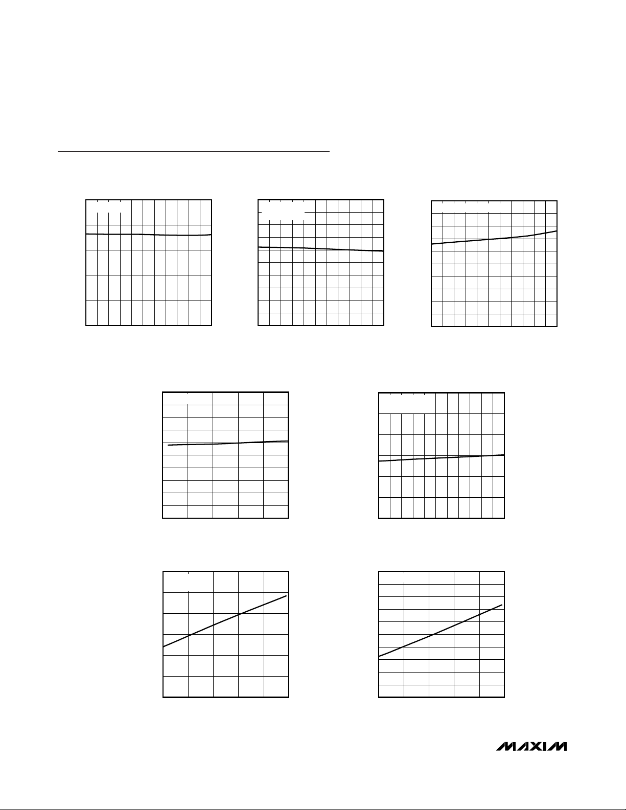
Typical Operating Characteristics
(VCC= +5V, V
I/O
= +3.3V. V
BAT
= +12V, RL= 60Ω, C
SPLIT
= 4700pF, TA = +25°C, unless otherwise noted.)
I
BAT
SUPPLY CURRENT
vs. TEMPERATURE
TEMPERATURE (°C)
I
BAT
(μA)
MAX13041 toc01
-40 -25 -10 5 20 35 50 65 80 95 110 125
0
5
10
15
20
25
SLEEP MODE
ICC SUPPLY CURRENT
vs. TEMPERATURE
TEMPERATURE (°C)
I
CC
(mA)
MAX13041 toc02
-40 -25 -10 5 20 35 50 65 80 95 110 125
0
5
10
15
20
25
30
35
40
45
50
NORMAL MODE
f
TXD
= 1Mbps
ICC SUPPLY CURRENT
vs. TEMPERATURE
TEMPERATURE (°C)
I
CC
(mA)
MAX13041 toc03
-40 -25 -10 5 20 35 50 65 80 95 110 125
0
1
2
3
4
5
6
7
8
9
10
PWON/LISTEN-ONLY MODE
ICC SUPPLY CURRENT
vs. TXD FREQUENCY
TXD FREQUENCY (kHz)
I
CC
(mA)
MAX13041 toc04
0 100 200 300 400 500
0
5
10
15
20
25
30
35
40
45
50
NORMAL MODE
I
I/O
SUPPLY CURRENT
vs. TEMPERATURE
TEMPERATURE (°C)
I
I/O
SUPPLY CURRENT (μA)
MAX13041 toc05
-40 -25 -10 5 20 35 50 65 80 95 110 125
0
50
100
150
200
250
300
NORMAL MODE
f
TXD
= 1Mbps
I
I/O
SUPPLY CURRENT vs. V
I/O
V
I/O
(V)
I
I/O
(5μA)
MAX13041 toc06
2.8 3.3 3.8 4.3 4.8 5.3
0
50
100
150
200
250
300
NORMAL MODE
f
TXD
= 1Mbps
I
I/O
SUPPLY CURRENT vs. V
I/O
V
I/O
(V)
I
I/O
(μA)
MAX13041 toc07
2.8 3.3 3.8 4.3 4.8 5.3
0
0.2
0.4
0.6
0.8
1.0
1.2
1.4
1.6
1.8
2.0
SLEEP MODE
Page 7
MAX13041
±80V Fault-Protected High-Speed CAN Transceiver
with Low-Power Management and Wake-On CAN
_______________________________________________________________________________________ 7
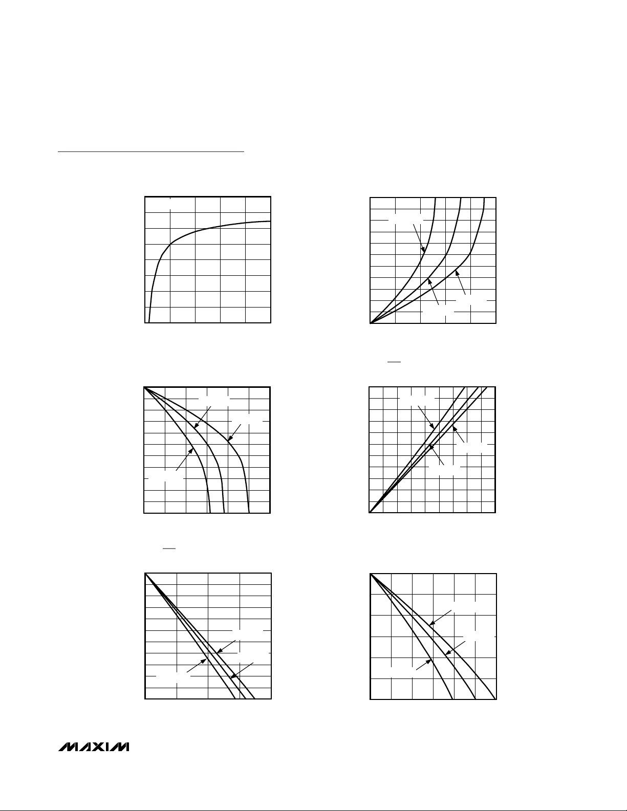
Typical Operating Characteristics (continued)
(VCC= +5V, V
I/O
= +3.3V. V
BAT
= +12V, RL= 60Ω, C
SPLIT
= 4700pF, TA = +25°C, unless otherwise noted.)
DIFFERENTIAL OUTPUT VOLTAGE
vs. LOAD RESISTANCE
3.6
NORMAL MODE
3.4
3.2
3.0
2.8
2.6
2.4
DIFFERENTIAL OUTPUT VOLTAGE (V)
2.2
2.0
0 200 400 600 800 1000
LOAD RESISTANCE (Ω)
RXD OUTPUT VOLTAGE HIGH
vs. OUTPUT CURRENT
3.3
3.0
2.7
2.4
2.1
1.8
1.5
1.2
TA = +125°C
0.9
OUTPUT VOLTAGE HIGH (V)
0.6
0.3
0
024681012
OUTPUT CURRENT (mA)
TA = +25°C
TA = -40°C
MAX13041 toc08
MAX13041 toc10
3.3
3.0
2.7
2.4
2.1
1.8
1.5
1.2
0.9
OUTPUT VOLTAGE LOW (V)
0.6
0.3
3.3
3.0
2.7
2.4
2.1
1.8
1.5
1.2
0.9
OUTPUT VOLTAGE LOW (V)
0.6
0.3
RXD OUTPUT VOLTAGE LOW
vs. OUTPUT CURRENT
TA = +125°C
TA = -40°C
TA = +25°C
0
0 5 10 15 20 25
OUTPUT CURRENT (mA)
ERR OUTPUT VOLTAGE LOW
vs. OUTPUT CURRENT
TA = +125°C
TA = -40°C
TA = +25°C
0
0 0.2 0.4 0.6 0.8 1.0 1.2 1.4 1.6 1.8
OUTPUT CURRENT (mA)
MAX13041 toc09
MAX13041 toc11
ERR OUTPUT VOLTAGE HIGH
vs. OUTPUT CURRENT
3.3
3.0
2.7
2.4
2.1
1.8
1.5
1.2
0.9
OUTPUT VOLTAGE HIGH (V)
0.6
TA = +125°C
0.3
0
0 50 100 150 200
OUTPUT CURRENT (μA)
TA = -40°C
TA = +25°C
MAX13041 toc12
12
10
8
6
INH VOLTAGE (V)
4
2
0
024681012
INH VOLTAGE
vs. SOURCE CURRENT
MAX13014 toc13
TA = -40°C
TA = +25°C
TA = +125°C
SOURCE CURRENT (mA)
Page 8

MAX13041
±80V Fault-Protected High-Speed CAN Transceiver
with Low-Power Management and Wake-On CAN
8 _______________________________________________________________________________________
Typical Operating Characteristics (continued)
(VCC= +5V, V
I/O
= +3.3V. V
BAT
= +12V, RL= 60Ω, C
SPLIT
= 4700pF, TA = +25°C, unless otherwise noted.)
INH VOLTAGE vs. TEMPERATURE
TEMPERATURE (°C)
INH VOLTAGE (V)
MAX13041 toc14
-40 -25 -10 5 20 35 50 65 80 95 110 125
10.0
10.2
10.4
10.6
10.8
11.0
11.2
11.4
11.6
11.8
12.0
I
INH
= 1mA
CAN-RXD PROPAGATION DELAY
vs. TEMPERATURE
TEMPERATURE (°C)
CAN-RXD PROP DELAY (ns)
MAX13041 toc15
-40 -25 -10 5 20 35 50 65 80 95 110 125
0
10
20
30
40
50
60
70
80
90
100
0.0
0.2
0.6
0.4
0.8
2.0
-40
20
5
65
95
125
SPLIT LEAKAGE
vs. TEMPERATURE
MAX13041 toc19
TEMPERATURE (°C)
SPLIT LEAKAGE (μA)
110
80
50
35
-10
-25
1.0
1.2
1.4
1.6
1.8
V
SPLIT
= +12V
TXD-CAN PROPAGATION DELAY
100
vs. TEMPERATURE
90
80
70
60
50
40
30
TXD-CAN PROP DELAY (ns)
20
10
0
-40 -25 -10 5 20 35 50 65 80 95 110 125
TEMPERATURE (°C)
MAX13041 toc16
TXD-CAN PROPAGATION DELAY
C
= 47μF
SPLIT
200ns/div
MAX13041 toc17
TXD
2V/div
CANH
1V/div
CANL
1V/div
CAN-RXD PROPAGATION DELAY
C
= 47μF
SPLIT
200ns/div
MAX13041 toc18
RXD
2V/div
CANH
1V/div
CANL
1V/div
Page 9

MAX13041
±80V Fault-Protected High-Speed CAN Transceiver
with Low-Power Management and Wake-On CAN
_______________________________________________________________________________________ 9
Pin Description
PIN NAME DESCRIPTION
1 TXD Data Transmit Input, CMOS Compatible. TXD is internally pulled up to V
2 GND Ground
3V
4 RXD Data Receive Output, CMOS Compatible
5V
6EN
7 INH Inhibit Output. INH controls one or more external voltage regulators.
8 ERR Error Output, Active Low. ERR indicates errors and displays status of internal flags.
9 WAKE Local Wake-Up Input. Present a voltage transition on WAKE to generate a local wake-up event.
10 V
11 SPLIT
12 CANL Low-Level CAN Differential Bus Line
13 CANH High-Level CAN Differential Bus Line
14 STB
CC
I/O
BAT
Supply Voltage +4.75V to +5.25V. Bypass V
possible to the device.
Supply Voltage for I/O Level Translation, +2.8V < V
to ground with a 0.1µF ceramic capacitor as close as possible to the device.
V
I/O
Enable Input. Control the operating mode by driving EN logic-high or logic-low (see Table 1 and
Figure 4.)
Battery Voltage Input. Bypass V
the device.
Split Termination Voltage Output. Connect SPLIT to the center node of two 60Ω termination resistors
to provide common-mode voltage stabilization (see Figure 3). SPLIT outputs a voltage of V
Standby Input, Active Low. Drive STB logic-high or logic-low to control the operating mode (see Table
1 and Figure 4.)
to ground with a 0.1µF ceramic capacitor as close as possible to
BAT
to ground with a 0.1µF ceramic capacitor as close as
CC
< VCC (see the Level Shifting section). Bypass
I/O
I/O
.
CC
/2.
Page 10

MAX13041
±80V Fault-Protected High-Speed CAN Transceiver
with Low-Power Management and Wake-On CAN
10 ______________________________________________________________________________________
Timing Diagrams
Figure 1. Timing Diagram
Figure 2. Test Circuit for Timing Characteristics
TXD
CANH
CANL
+5V
V
t
D(TXD-BUSON)
V
I(DIF)(BUS)
47μF
+
I(DIF)(BUS)
RXD
100nF
= V
CANH
- V
CANL
TXD
EN
STB
WAKE
DOMINANT
0.3 V
I/O
t
D(BUSON - RXD)
V
I/O
MAX13041
GND
0.9V
0.5V
RECESSIVE
HIGH
0.7 V
I/O
LOW
t
D(TXD-BUSOFF)
t
D(BUSOFF - RXD)
+12V
+
10μF
V
V
BAT
CC
CANH
60Ω
CANL
SPLIT
ERR
INH
RXD
100pF
15pF
Page 11

Detailed Description
The MAX13041 ±80V fault-protected, high-speed CAN
transceiver is intended for high-speed industrial and
automotive network applications where high reliability
and advanced power management are required. The
device links a CAN protocol controller to the physical
bus wires of the controller area network (CAN) and
allows communication at speeds up to 1Mbps. Built-in
level shifting allows for direct connection to protocol controllers operating from lower voltages. The extended
fault-protected voltage range of ±80V on CAN bus lines
allows for use in +12V or +42V automotive, and higher
voltage +24V and +36V heavy-duty truck applications.
Advanced power management features make the
MAX13041 ideal for automotive electronic control unit
(ECU) modules that are permanently supplied by battery, regardless of the ignition switch position (clamp30, type-A modules). The device controls one or more
external voltage regulators to provide a low-power
sleep mode for an entire clamp-30 node. Wake-on CAN
capability allows the MAX13041 to restore power to the
node upon detection of CAN bus activity. The
MAX13041 is functionally compatible with the Philips
TJA1041A and is a pin-to-pin replacement with
improved performance.
CAN Interface
The ISO11898 specification describes the physical
layer of a controller area network (CAN). A CAN implementation is comprised of multiple transceiver modules
linked by a pair of bus wires. Communication between
modules occurs through transmission and reception of
differential logic states on the bus lines. Two complimentary logic states are defined by ISO11898. A dominant state results when the differential voltage on the
CAN bus lines is greater than 0.9V. A recessive bus
state results when the differential voltage is less than
0.5V (Figure 1). The CAN bus exhibits a wired-AND
characteristic, meaning the bus is only recessive when
all connected transmitters are recessive. Any transmitter asserting a dominant logic state forces the entire
CAN bus dominant.
The MAX13041 accepts logic-level data from the CAN
protocol controller on TXD. Drive TXD low to assert a
dominant state on the CAN bus. Drive TXD high to
release the CAN bus to a recessive state. TXD is internally pulled up to V
I/O
. The state of the CAN bus is presented to the protocol controller as a logic level on
RXD. The MAX13041 receiver remains active during
transmission to allow for the bit-wise arbitration scheme
specified by the CAN protocol.
Level Shifting
The MAX13041 provides level shifting on TXD, RXD,
EN, STB, WAKE and ERR for compatibility with lowervoltage protocol controllers. Set the interface logic levels for TXD, RXD, EN, STB, WAKE, and ERR by
connecting V
I/O
to the supply voltage of a CAN protocol
controller, or another voltage from +2.8V to +5.25V.
Split-Termination and Common-Mode
Voltage Stabilization
The CAN bus specification requires a total bus load resistance of 60Ω. Each end of the bus should be terminated
with 120Ω, the characteristic impedance of the bus line.
Electromagnetic emission (EME) is reduced by a split-termination method, whereby each end of the bus line is terminated by 120Ω split into two 60Ω resistors in series
(see Figure 3). A bypass capacitor shunts noise to
ground from the node connecting the 60Ω resistors.
When the CAN bus is recessive, the common-mode
voltage is pulled low by the leakage current from inactive modules. When the CAN bus subsequently goes
dominant, the proper common-mode voltage is
restored by the transmitting device. A common-mode
voltage step results, generating excessive EME. To mitigate this problem, the common-mode voltage of the
bus is forced to VCC/2 by biasing the split-termination
node (see Figure 3). During normal and PWON/listenonly modes, a stabilized DC voltage of VCC/2 is present
on SPLIT. Connect SPLIT to the node connecting the
two 60Ω termination resistors to stabilize the commonmode voltage of the bus and prevent EME from common-mode voltage steps.
Power-Management Operating Modes
The MAX13041 provides advanced power management
for a clamp-30 node by controlling one or more external
voltage regulators. Five operating modes provide different functionality to minimize power consumption.
MAX13041
±80V Fault-Protected High-Speed CAN Transceiver
with Low-Power Management and Wake-On CAN
______________________________________________________________________________________ 11
Figure 3. Biased Split Termination
CANH
R
T
60Ω
SPLIT
C
SPLIT
CANL
R
T
60Ω
Page 12

MAX13041
In the lowest-power mode, the MAX13041 disables external voltage regulators to provide a sleep mode for the
entire node. The MAX13041 restores power to the node
upon a logic transition on WAKE or detection of CAN
bus activity.
The operating mode is determined by an internal state
machine controlled by EN and STB, as well as several
internal flags (see Table 1 and Figure 4).
Normal Mode
The MAX13041 provides full bidirectional CAN communication in normal mode. Drive TXD to transmit data on
the differential CAN bus lines CANH and CANL. The
CAN bus state is presented on RXD, a level-shifted
logic output. SPLIT is biased to VCC/2 to allow CAN bus
common-mode stabilization. INH is logic-high, enabling
one or more external voltage regulators (see Table 1).
PWON/Listen-Only Mode
In PWON/listen-only mode, the CAN transmitter is disabled. The CAN receiver remains active and the CAN
bus state is presented on RXD, a level-shifted logic output. As in normal mode, SPLIT is biased to VCC/2 to
allow CAN bus common-mode stabilization. INH is
logic-high, enabling one or more external voltage regulators (see Table 1).
Standby Mode
Standby mode is the first low-power operating mode.
The CAN transmitter and receiver are disabled, and a
low-power receiver is enabled to monitor the CAN bus
for activity. To reduce power consumption, commonmode stabilization is disabled. SPLIT becomes high
impedance, and CANH and CANL are biased to
ground by the termination resistors. INH remains logichigh, enabling one or more external voltage regulators
(see Table 1).
Go-to-Sleep Command Mode
Go-to-sleep command mode is part of the controlled
sequence for entering sleep mode. The MAX13041
remains in go-to-sleep command mode for a hold time of
56µs (max), and subsequently enters sleep mode if no
wake events are detected. During the hold time, if the
state of EN or STB changes, or if the UV
BAT
, PWON, or
wake-up flags are set, the go-to-sleep sequence is
aborted. During go-to-sleep command mode, functionality is the same as in standby mode.
Sleep Mode
Sleep mode is the lowest-power operating mode. The
CAN transmitter and receiver are disabled, and a lowpower receiver is enabled to monitor the CAN bus for
±80V Fault-Protected High-Speed CAN Transceiver
with Low-Power Management and Wake-On CAN
12 ______________________________________________________________________________________
Table 1. Operating Modes
Note 6: Setting the PWON or wake-up flags clears UVNOM flag.
Note 7: The MAX13041 enters sleep mode from any other mode when UVNOM is set. INH becomes high impedance.
Note 8: When go-to-sleep command mode is selected for longer than tH(MIN), the MAX13041 enters sleep mode.
INH becomes high impedance.
Note 9: PWON and wake-up flags are cleared upon entering normal mode.
CONTROL PINS INTERNAL FLAGS
STB EN UV
XX
L H CLEAR CLEAR
H L CLEAR CLEAR X PWON/LISTEN-ONLY H
H H CLEAR CLEAR X NORMAL (Note 9) H
NOM
SET X X SLEEP (Notes 6, 7) FLOATING
CLEAR SET
UV
BAT
PWON, WAKE-UP
EITHER FLAG SET STANDBY H
BOTH FLAGS CLEAR STANDBY FROM ANY OTHER MODE H
EITHER FLAG SET STANDBY H
BOTH FLAGS CLEAR
EITHER FLAG SET STANDBY H
BOTH FLAGS CLEAR
NO CHANGE FROM SLEEP MODE FLOATINGL L CLEAR CLEAR
STANDBY FROM ANY OTHER MODE H
NO CHANGE FROM SLEEP MODE FLOATING
GO-TO-SLEEP COMMAND MODE FROM
ANY OTHER MODE (Note 7)
OPERATING MODE INH
H
Page 13

activity. To reduce power consumption, common-mode
stabilization is disabled. SPLIT becomes high impedance, and CANH and CANL are biased to ground by
the termination resistors. INH goes high impedance,
disabling one or more external voltage regulators (see
Table 1.)
Flag Signaling
The MAX13041 uses a set of seven internal flags for
system diagnosis and to indicate faults. Five of the
flags are available at different times to the CAN protocol controller on ERR. A logic-low on ERR indicates a
set flag or a fault (see Table 3.) Allow ERR to stabilize
for at least 8µs after changing operating modes.
Supply Undervoltage: UV
NOM
UV
NOM
is set when supply voltage on VCCdrops below
V
CC(SLEEP)
for longer than t
UV(Vcc),
or when voltage on
V
I/O
drops below V
I/O(SLEEP)
for longer than t
UV(VI/O)
.
When UV
NOM
is set, the MAX13041 enters low-power
sleep mode to reduce power consumption. The device
remains in sleep mode for a minimum waiting time
before allowing the UV
NOM
flag to be cleared. This
waiting time is determined by the same timer used for
setting UV
NOM(tUV(VCC)
or t
UV(VIO)
.) UV
NOM
is cleared
by a local wake-up request triggered by a level change
on WAKE or by a wake-on-CAN event. UV
NOM
is also
cleared by setting the PWON flag.
V
BAT
Undervoltage: UV
BAT
UV
BAT
is set when the voltage on V
BAT
drops below
V
BAT(STB)
. When UV
BAT
is set, the MAX13041 enters
standby mode to reduce power consumption. UV
BAT
is
cleared when the voltage on V
BAT
is restored and
exceeds V
BAT(STB)
. Upon clearing UV
BAT
, the
MAX13041 returns to the operating mode determined
by EN and STB.
Power-On Flag: PWON
PWON indicates the MAX13041 is in a power-on state.
PWON is set when V
BAT
has dropped below V
BAT(STB)
and has subsequently recovered. This condition occurs
MAX13041
±80V Fault-Protected High-Speed CAN Transceiver
with Low-Power Management and Wake-On CAN
______________________________________________________________________________________ 13
Figure 4. State Diagram
STB = H AND EN = H
STB = H
AND EN = L
STANDBY MODE
STB = L
AND
(EN = L OR
FLAG SET)
STB = H
AND EN = L
STB = H AND EN = L
STB = L
AND EN = L
STB = L AND EN = H
AND FLAGS CLEARED
STB = L AND
(EN = L OR FLAG SET)
STB = H
AND EN = H
STB = L AND EN = H
AND FLAGS CLEARED
NORMAL MODEPWON/LISTEN-ONLY MODE
STB = H
AND EN = H
STB = L
AND EN = H
GO-TO-SLEEP COMMAND MODE
STB = L AND
FLAG SET
LOGIC STATE OF EN OR STB
SETTING PWON AND/OR WAKE-UP FLAG.
PWON AND WAKE-UP FLAG BOTH CLEARED.
STB = H AND EN = L
AND UV
CLEARED
NOM
NOTES: H AND L ARE
FLAG SET =
FLAGS CLEARED
SLEEP MODE
FLAGS CLEARED
AND t > t
H(MIN)
STB = H AND EN = H
NOM
CLEARED
AND UV
Page 14

MAX13041
when battery voltage is first applied to V
BAT
. When the
PWON flag is set, UV
NOM
is cleared and sleep mode is
disabled. The primary function of the PWON flag is to prevent the MAX13041 from entering sleep mode (and thereby disabling external voltage regulators) before the
protocol controller establishes control through EN and
STB. The PWON flag is externally indicated as a logic-low
on ERR when the MAX13041 is placed into PWON/listenonly mode from standby mode, go-to-sleep command
mode, or sleep mode. The PWON flag is cleared when
the MAX13041 enters normal mode.
Wake-Up Flag
The wake-up flag is set when a local or remote wake-up
request is detected. A local wake-up request is generated when the logic level on WAKE changes and
remains stable for t
WAKE
. A remote wake-on CAN
request is generated upon the detection of two dominant bus cycles, each followed by a recessive bus
cycle (see Figure 5.) Each bus cycle must exceed
t
BUS(DOM)
. The wake-up flag can only be set in standby mode, go-to-sleep command mode, or sleep mode.
Setting the wake-up flag resets UV
NOM
, and wake-up
requests are not detected during the UV
NOM
flag wait-
ing time immediately after UV
NOM
has been set. The
wake-up flag is immediately available as a logic-low on
ERR and RXD, provided that V
I/O
and VCCare both
present. The wake-up flag is cleared when the
MAX13041 enters normal mode.
Wake-Up Source Flag
The wake-up source flag is set concurrently with the
wake-up source flag when a local wake-up event is
detected. The wake-up source flag can only be set
after the PWON flag has been cleared. The flag is
cleared when the MAX13041 leaves normal mode and
during initial power-on. The wake-up source flag is
externally indicated on ERR when the MAX13041 is in
±80V Fault-Protected High-Speed CAN Transceiver
with Low-Power Management and Wake-On CAN
14 ______________________________________________________________________________________
Figure 5. Wake-On-CAN Timing
Table 2. Flag Signaling on ERR
Note 10: Allow for a dominant time of at least 4µs per dominant-recessive cycle.
INTERNAL FLAG FLAG AVAILABLE ON ERR CONDITIONS TO CLEAR FLAG
UV
NOM
UV
BAT
PWON
Wake-Up
Wake-Up Source
Bus Failure
Local Failure
No Set PWON or wake-up flags
No Recovery of V
In PWON/listen-only mode (changing from
standby, go-to-sleep command, or sleep modes)
In standby, go-to-sleep command, and sleep
modes (provided V
In normal mode (before the fourth dominant to
recessive edge on TXD, Note 10)
In normal mode (after the fourth dominant to
recessive edge on TXD, Note 10)
In PWON/listen-only mode (coming from normal
mode)
and VCC are present)
I/O
Entering normal mode
Entering normal mode or setting PWON or UV
flag
Leaving normal mode or setting PWON flag
Re-entering normal mode
Entering normal mode or whenever RXD is
dominant while TXD is recessive (and all local
failures are resolved)
BAT
NOM
DOMINANT
CANH
CANL
t
BUSDOM
RECESSIVE
t
BUSDOM
DOMINANT
RECESSIVE
t
BUSDOM
t
BUSDOM
Page 15

normal mode, prior to the fourth dominant-to-recessive
transition on TXD. A low level on ERR indicates a local
wake-up has occurred.
Bus Failure Flag
The bus failure flag is set when the MAX13041 detects
a CAN bus short-circuit to V
BAT
, V
CC,
or GND for four
consecutive dominant-recessive cycles on TXD. The
flag is cleared when the MAX13041 leaves normal
mode. The bus failure flag is externally indicated as a
logic low on ERR in normal mode, after the fourth dominant-to-recessive transition on TXD.
Local Failure Flag
The local failure flag indicates five separate local failure
conditions (see
Fault Protection & Fail-Safes
section).
When one or more local failure conditions have
occurred, the local failure flag is set. The flag is cleared
when the MAX13041 enters normal mode or when RXD
goes logic-low while TXD is logic-high. The local failure
flag is externally indicated as a logic-low on ERR when
the MAX13041 is placed into PWON/listen-only mode
from normal mode.
Wake-On CAN
The MAX13041 provides wake-on-CAN capability from
sleep mode. When the MAX13041 detects two dominant bus states, each followed by a recessive state
(Figure 5), the MAX13041 sets the wake-up flag and
enters an operating mode determined by the state of
EN and STB. Each CAN logic state must be at least 5µs
in duration. This wake-up detection criterion serves to
prevent unintentional wake-up events due to bus faults
such as V
BAT
to CANH or an open circuit on CANL. At
higher data rates (>125kbit/s), wake-up can not be
guaranteed for a single, arbitrary CAN data frame. Two
or more consecutive arbitrary CAN data frames may be
required to ensure a successful wake-on-CAN event.
External-Voltage Regulator Control
MAX13041 controls one or more external voltage regulators through INH, a V
BAT
-referenced, open-drain output. When INH is logic-high, any external voltage
regulators are active and power is supplied to the
node. When INH is high-impedance, the typical pulldown characteristic of the voltage-regulator inhibit input
pulls INH to a logic-low and disables the external voltage regulator(s).
Fault Protection & Fail-Safes
The MAX13041 features ±80V tolerance on CAN bus
lines CANH, CANL, and SPLIT. Up to +76V operation is
possible on V
BAT
, allowing for use in +42V automotive
applications. Additionally, the device detects local and
remote bus failures and features fail-safe modes to
prevent damage to the device or interference with CAN
bus communication.
The MAX13041 detects five different local faults. When
any local fault is detected, the local failure flag is set.
Additionally, for faults other than bus dominant clamping, the transmitter is disabled to prevent possible damage to the device. The transmitter remains disabled
until the local failure flag is cleared.
TXD Dominant Clamping
An extended logic-low level on TXD due to hardware or
software failure would ordinarily clamp the CAN bus to
a dominant state, blocking communication on the entire
bus. This condition is prevented by the TXD dominant
time-out feature. If TXD is held low for longer than
t
DOM(TXD)
, the local failure flag is set and the transmitter is disabled until the local failure flag is cleared. The
TXD time-out value limits the minimum allowable bit rate
to 40kbps.
RXD Recessive Clamping
If a hardware failure clamps RXD to a logic-high level,
the protocol controller assumes the CAN bus is in a
recessive state at all times. This has the undesirable
effect that the protocol controller assumes the bus is
clear and may initiate messages that would interfere with
ordinary communication. This local failure is detected by
checking the state of RXD when the CAN bus is in a
dominant state. If RXD does not reflect the state of the
CAN bus, the local failure flag is set and the transmitter is
disabled until the local failure flag is cleared.
TXD-to-RXD Short-Circuit Detection
A short-circuit between TXD and RXD forces the bus
into a permanent dominant state upon the first transmission of a dominant bit because normally the low-side
driver of RXD is stronger than the microcontroller highside driver of TXD. The MAX13041 detects this condition and prevents the resulting bus failure by setting the
local failure flag and disabling the transmitter. The
transmitter remains disabled until the local failure flag is
cleared.
Bus Dominant Clamping
A short-circuit fault from the CAN bus to V
BAT
, VCC, or
GND could produce a differential voltage between
CANH and CANL greater than the receiver threshold,
resulting in a dominant bus state. If the bus state is
clamped dominant for longer than t
DOM(BUS)
, the local
failure flag is set. The transmitter is not disabled by this
fault and the local failure flag is cleared as soon as the
bus state becomes recessive.
MAX13041
±80V Fault-Protected High-Speed CAN Transceiver
with Low-Power Management and Wake-On CAN
______________________________________________________________________________________ 15
Page 16

MAX13041
Thermal Shutdown Fault
The local failure flag is set when the junction temperature
(TJ) exceeds the shutdown junction temperature threshold, T
J(SD)
. The transmitter is disabled to prevent excessive current dissipation from damaging the device. The
transmitter remains disabled until T
J
drops T
J(SD)HYST
degrees, and the local failure flag is cleared.
Recovering from Local Faults
The local failure flag is cleared and the transmitter is reenabled whenever RXD is dominant while TXD is recessive. This situation occurs normally when the MAX13041
is receiving CAN bus data in the absence of a bus failure.
In PWON/listen-only mode, ERR changes to a logic-high
to reflect the change in the local failure flag. If there is no
activity on the CAN bus, the local failure flag can also be
cleared by switching to normal mode from another operating mode. A typical method involves switching to
PWON/listen-only mode and reading the local failure flag
on ERR. Subsequently, switch back to normal mode to
clear the flag. This sequence is then repeated to verify
that the failure has been resolved.
ESD Protection
As with all Maxim devices, ESD-protection structures
are incorporated on all pins to protect against electrostatic discharges encountered during handling and
assembly. The CANH and CANL lines are further protected by advanced ESD structures to guard these pins
from damage caused by ESD of up to ±12kV as measured by the Human Body Model (HBM). Protection
structures prevent damage caused by ESD events in all
operating modes, and when the device is unpowered.
ESD Models
Several ESD testing standards exist for gauging the
robustness of ESD structures. The ESD protection of
the MAX13041 is characterized for the human body
model (HBM). Figure 6 shows the model used to simulate an ESD event resulting from contact with the
human body. The model consists of a 100pF storage
capacitor that is charged to a high voltage, and subsequently discharged through a 1.5kΩ resistor. Figure 7
shows the current waveform when the storage capacitor is discharged into a low impedance.
ESD Test Conditions
ESD performance depends on a variety of conditions.
Please contact Maxim for a reliability report documenting test setup, methodology, and results.
Applications Information
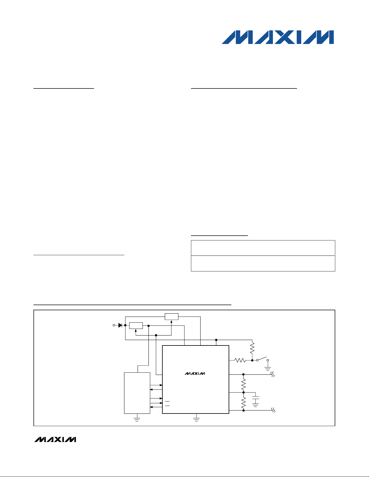
Clamp-30, Type-A CAN Modules
The MAX13041 is primarily intended for automotive
ECU applications where battery power is permanently
supplied to the node (see Figure 8.) This type of application is referred to as a clamp-30 node. ECU modules,
which are supplied by the battery only when the ignition
switch is closed, are referred to as clamp-15 modules.
Because clamp-30 modules are permanently supplied
by battery voltage, low power consumption is an essential design requirement. The MAX13041 provides
advanced power management to the entire node by
controlling one or more external voltage regulators.
While CAN transceivers, such as the MAX13041,
operate from a supply voltage of +5V, many microprocessors are supplied by voltages of +3.3V and
lower. By controlling the supply voltage regulator for the
microprocessor, the MAX13041 can force a low-power
sleep mode for the entire node.
EMC Considerations
In multidrop CAN applications, it is important to maintain a direct point-to-point wiring scheme. A single pair
of wires should connect each transceiver on the CAN
bus, and the bus wires should be properly split-terminated with two 60Ω resistors at each end as described
in Figure 3 . For best EMC performance, do not use a
star topology. Any deviation from the point-to-point
wiring scheme results in a stub. High-speed edges of
the CAN signal reflect from the unterminated stub ends,
interfering with communication on the bus. To minimize
the effect of these reflections, care should be taken to
minimize the length of stubs.
Power-Supply Decoupling
Bypass VCC, V
BAT
, and V
I/O
to ground with 0.1µF
ceramic capacitors. Place all capacitors as close as
possible to the device.
±80V Fault-Protected High-Speed CAN Transceiver
with Low-Power Management and Wake-On CAN
16 ______________________________________________________________________________________
Page 17

MAX13041
±80V Fault-Protected High-Speed CAN Transceiver
with Low-Power Management and Wake-On CAN
______________________________________________________________________________________ 17
Figure 6. Human Body ESD Test Model
Figure 7. Human Body Model Current Waveform
Figure 8. Typical ECU Architecture with Clamp-30 and Clamp-15 Modules
R
D
1.5kΩ
DISCHARGE
RESISTANCE
STORAGE
CAPACITOR
HIGH-
VOLTAGE
DC
SOURCE
R
C
1MΩ
CHARGE-CURRENT-
LIMIT RESISTOR
C
s
100pF
V
BAT
MAX13041
CLAMP 30
MAX13041
DEVICE
UNDER
TEST
MAX13041
PEAK-TO-PEAK RINGING
I
r
(NOT DRAWN TO SCALE)
AMPERES
IP 100%
90%
36.8%
10%
0
0
t
RL
TIME
t
DL
CURRENT WAVEFORM
CLAMP 15
IGNITION
SWITCH
CLAMP 15
CAN NODE
CLAMP 15
CAN NODE
Page 18

MAX13041
±80V Fault-Protected High-Speed CAN Transceiver
with Low-Power Management and Wake-On CAN
18 ______________________________________________________________________________________
Pin Configuration
Chip Information
PROCESS: BiCMOS
TOP VIEW
TXD
1
GND
2
3
V
CC
4
V
5
I/O
EN
6
7
+
MAX13041
SO
14
STB
13
CANH
12
CANL
11
SPLITRXD
10
V
BAT
9
WAKE
ERRINH
8
Page 19

MAX13041
±80V Fault-Protected High-Speed CAN Transceiver
with Low-Power Management and Wake-On CAN
______________________________________________________________________________________ 19
Functional Diagram
INH
TXD
RXD
ERR
STB
WAKE
V
I/O
LEVEL
SHIFTING
EN
V
BAT
V
CC
FLAG
SIGNALING
OPERATING
MODE
CONTROL
WAKE
DETECT
MAX13041
LOW POWER
RECEIVER
COMMON-
MODE
STABILIZATION
CANH
CANL
SPLIT
GND
Page 20

MAX13041
±80V Fault-Protected High-Speed CAN Transceiver
with Low-Power Management and Wake-On CAN
20 ______________________________________________________________________________________
Package Information
(The package drawing(s) in this data sheet may not reflect the most current specifications. For the latest package outline information,
go to www.maxim-ic.com/packages
.)
N
1
TOP VIEW
e
FRONT VIEW
INCHES
DIM
MIN
0.053A
0.004
A1
0.014
B
0.007
C
e 0.050 BSC 1.27 BSC
0.150
HE
D
A
B
A1
C
L
E
H 0.2440.228 5.80 6.20
0.016L
VARIATIONS:
INCHES
MINDIM
D
0.189 0.197 AA5.004.80 8
0.337 0.344 AB8.758.55 14
D
0∞-8∞
MAX
0.069
0.010
0.019
0.010
0.157
0.050
MAX
0.3940.386D
MILLIMETERS
MAX
MIN
1.35
1.75
0.10
0.25
0.35
0.49
0.19
0.25
3.80 4.00
0.40 1.27
MILLIMETERS
MAX
MIN
9.80 10.00
N MS012
16
AC
SOICN .EPS
SIDE VIEW
PROPRIETARY INFORMATION
TITLE:
PACKAGE OUTLINE, .150" SOIC
REV.DOCUMENT CONTROL NO.APPROVAL
21-0041
1
B
1
Page 21

MAX13041
±80V Fault-Protected High-Speed CAN Transceiver
with Low-Power Management and Wake-On CAN
Maxim cannot assume responsibility for use of any circuitry other than circuitry entirely embodied in a Maxim product. No circuit patent licenses are
implied. Maxim reserves the right to change the circuitry and specifications without notice at any time.
Maxim Integrated Products, 120 San Gabriel Drive, Sunnyvale, CA 94086 408-737-7600 ____________________
21
© 2007 Maxim Integrated Products is a registered trademark of Maxim Integrated Products, Inc.
Boblet
Revision History
REVISION
NUMBER
REVISION
DATE
DESCRIPTION
PAGES
CHANGED
0 2/07 Initial release —
1 11/07 Notes changed in EC Table 2–5,12
 Loading...