

Page 1
ADVANCED DATASHEET
VDD
BS TXS
PRXON
ANT
GND
2 V Dual-Mode WCDMA & Dual Band GSM/DCS SP5T Switch MASWSS0049
VER 1. 0.5 – 2.0 GHz
Rev 1.1
Features
• GSM Power Handling with +2.0 V Control
Voltage
• Low Power Consumption. Less than 1µA in Rx
Mode.
• Integrated Low Loss Diplexer.
• Integrated Decoder.
• Leadless 5x 5 mm FQFP -N, 20 Pin Package.
• Low Insertion Loss, 0.8 dB in GSM Transmit
Mode.
• Excellent Harmonic Characteristics.
Description
The M/A-COM MASWSS0049 is a GaAs
monolithic switch in a low cost, FQFP -N, surface
mount plastic package. The MASWSS0049 is
ideally suited for applications where very low
power consumption, high power handling, and low
cost are required. The MASWSS0049 includes an
integrated decoder and a low loss diplexer. The
switch offers GSM power handling with below
+2.5V control voltage. The supply voltage VDD
should be connected to the highest available
voltage.
The MASWSS0049 is fabricated using a new 0.5micron gate length GaAs pHEMT process. The
process features full chip passivation for increased
performance and reliability. This switch is designed
for Dual Mode WCDMA/GSM/DCS handsets
where the phone needs to be able to simultaneously
receive a WCDMA and GSM signal.
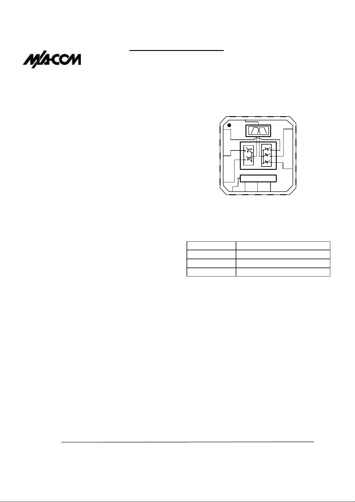
Functional Schematic
GND
GND
GND
WCDMA
GND
GRX
DRX
DRXS
GND
GND
GTX
Decoder
DTX
GND
GND
Ordering Information
Part Number Description
MASWSS0049-XFLT1 MASWSS0049 on 1000 Piece Tape and Reel
MASWSS0049-XFLT3 MASWSS0049 on 3000 Piece Tape and Reel
MASWSS0049-XFLS0 MASWSS0049 Sample Test Board
* If specific reel size is required, consult factory for part number
assignment
The Advanced Specifica tions Data Sheet Contains Typical Electrical Specifications Which May Change Prior to Final Introduction.
M/A-COM, Inc.
North America: Tel. (800) 366-2266 ♦ Asia/Pacific: Tel. +81 3 3263-8761 ♦ Europe: Tel. +44 (1344) 869-595
Fax (800) 618-8883 Fax +81 3 3263-8769 Fax +44 (1344) 300 -020
1
Page 2
2V Control, Dual -Mode WCDMA & Dual Band GSM/DCS Tx/Rx SP5T Switch MASWSS0049
> DCS RX
> GSM TX
> DCS TX
V1.1
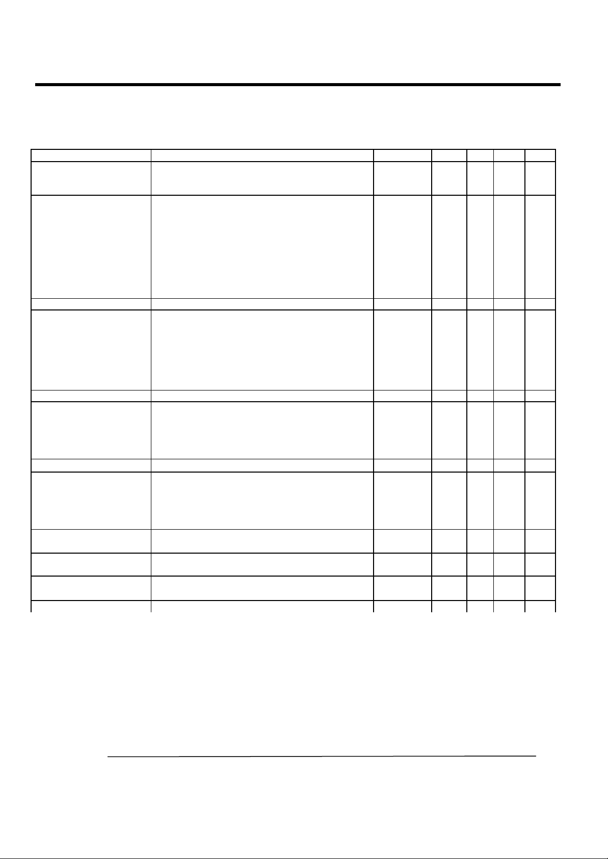
ELECTRICAL CHARACTERISTICS: Test Conditions: VDD = 2.5V, Vctrl =2.0V, T
= +25 °C
A
Mode Specifications Freq. (MH z) Units Min. Typ. Max.
ANT -> GSM RX
ANT -> UMTS Tx
ANT -> UMTS Rx
Isolation ANT to DCS Tx
ANT Isolation ANT to DCS Tx
Insertion Loss
Insertion Loss
Insertion Loss
Isolation ANT to GSM Tx
Isolation UMTS to DCS Rx
Isolation UMTS to GSM Rx
Isolation UMTS to GSM Tx
Isolation DCS Tx to DCS Rx
Isolation DCS Tx to GSM Rx
Isolation GSM Tx to DCS Rx
Isolation GSM Tx to GSM Rx
925 -960
1920-1980
2110-2170
1710-1785
880 – 915
1920 –1980
1920 –1980
1920 –1980
1710 – 1785
1710 – 1785
880 – 915
880 - 915
dB
dB
dB
dB
dB
dB
dB
dB
dB
dB
dB
dB
1.3
1.4
1.25
22
17
30
30
30
30
30
30
18
Insertion Loss 1805 -1880 dB 1.45
Isolation ANT to GSM Tx
Isolation DCS Tx to DCS Rx
Isolation DCS Tx to GSM Rx
Isolation GSM Tx to DCS Rx
Isolation GSM Tx to GSM Rx
1710 – 1785
880 – 915
1710 – 1785
1710 – 1785
880 – 915
880 - 915
dB
dB
dB
dB
dB
dB
24
13
25
30
30
30
ANT Isolation GSM Tx to UMTS
ANT Isolation DCS Tx to UMTS
2nd Harmonics
3rd Harmonics
Insertion Loss 880 – 915 dB 0.8
Isolation GSM Tx to DCS Rx
Isolation GSM Tx to GSM Rx
Isolation DCS Tx to DCS Rx
Isolation DCS Tx to GSM Rx
880 – 915
880 – 915
880 – 915
1710 – 1785
1710 – 1785
dB
dB
dB
dB
dB
30
30
25
30
30
Insertion Loss 1710 –1785 dB 1.4
Isolation DCS Tx to DCS Rx
Isolation DCS Tx to GSM Rx
Isolation GSM Tx to DCS Rx
Isolation GSM Tx to GSM Rx
Freq = 900 MHz, Input Power = +34 dBm
Freq = 1810 MHz, Input Power = +32 dBm
Freq = 900 MHz, Input Power = +34 dBm
Freq = 1810 MHz, Input Power = +32 dBm
1710 –1785
1710 –1785
1710 –1785
880 – 915
880 – 915
dBc
dBc
dB
dB
dB
dB
dB
dBc
dBc
25
30
30
30
30
-90
-74
-80
-76
Supply Voltage Volts 2.5
High Control Voltages Volts 2.0 2.5
Low Control Voltages Volts 0
1. DC blocking capacitors are required on all RF and shunt ports.
2. All impedances are 50 ohms
The Advanced Specifications Data Sheet Contains Typical Electrical Specifications Which May Change Prior to Final Introduction.
M/A-COM, Inc.
North America: Tel. (800) 366-2266 ♦ Asia/Pacific: Tel. +81 3 3263-8761 ♦ Europe: Tel. +44 (1344) 869 -595
Fax (800) 618-8883 Fax +81 3 3263-8769 Fax +44 (1344) 300 -020
2
Page 3

2V Control, Dual -Mode WCDMA & Dual Band GSM/DCS Tx/Rx SP5T Switch MASWSS0049
VDD
B
S TXS
PRXON
GND
Decoder
V1.1
Pin Configuration
Pin No. Pin Name Description
1
WCDMA WCDMA Port
2
GND RF Ground
3
GRX GSM Rx Port
4
GND RF Ground
5
GTX GSM Tx Port
6
VDD Decoder Vdd
7
BS Control 1
8
TXS Control 2
9
PRXON Control 3
10
GND RF Ground
11
GND RF Ground
12
DTX DCS Tx Port
13
GND RF Ground
14
DRXS DCS Rx Shunt
15
DRX DCS Rx Port
16
GND RF Ground
17
GND RF Ground
18
GND RF Ground
19
ANT Antenna
20
GND RF Ground
21
GND Paddle
Block Diagram
WCDMA
GND
GRX
GND
GTX
GND ANT GND
GND
DRX
DRXS
GND
DTX
GND
GND
Truth Table
BS TXS PRXON MODE
0 0 0
0 1 0 GSM TX – ANT
1 1 0 DCS TX – ANT
1 0 0 DCS RX – ANT
Logic Level Voltage Level
VLo “0”= 0 V
VHi “1”= 2.5 V
GSM RX – ANT
WCDMA – ANT
The Advanced Specifications Data Sheet Contains Typical Electrical Specifications Which May Change Prior to Final Introduction.
M/A-COM, Inc.
North America: Tel. (800) 366-2266 ♦ Asia/Pacific: Tel. +81 3 3263-8761 ♦ Europe: Tel. +44 (1344) 869 -595
Fax (800) 618-8883 Fax +81 3 3263-8769 Fax +44 (1344) 300 -020
3
Page 4

2V Control, Dual -Mode WCDMA & Dual Band GSM/DCS Tx/Rx SP5T Switch MASWSS0049
C7 BS
C4 C5 C6
C3
Decoder
V1.1
Sample Board Schematic
ANT
WCDMA
C1
DRX
GRX
C2
GTX
VDD
TXS PRXON
External Circuitry Parts List (Note: Values of external elements not final)
Ref. Designation Value Purpose
C1 22 pF DC Block
C2 22 pF DC Block
C3 22 pF DC Block
C4 22 pF DC Block
C5 4.7 pF RF Shunt
C6 22 pF DC Block
C7 22 pF DC Block
DTX
The Advanced Specifications Data Sheet Contains Typical Electrical Specifications Which May Change Prior to Final Introduction.
M/A-COM, Inc.
North America: Tel. (800) 366-2266 ♦ Asia/Pacific: Tel. +81 3 3263-8761 ♦ Europe: Tel. +44 (1344) 869 -595
Fax (800) 618-8883 Fax +81 3 3263-8769 Fax +44 (1344) 300 -020
4
Page 5

2V Control, Dual -Mode WCDMA & Dual Band GSM/DCS Tx/Rx SP5T Switch MASWSS0049
V1.1
MASWSS0049 Harmonics at the GSM TX Port versus Voltage
0
-20
-40
dBc
-60
-80
-100
2.2 2.4 2.6 2.8 3 3.2 3.4 3.6 3.8 4
MASWSS0049 Harmonics at the DCS TX Port versus Voltage
0
-20
-40
dBc
-60
Pin = 34 dBm, Vcontrol=2V
Vdd (V)
Pin = 32 dBm, Vcontrol=2V
GSM 2H
GSM 3H
DCS 2H
DCS 3H
-80
-100
2.2 2.4 2.6 2.8 3 3.2 3.4 3.6 3.8 4
MASWSS0049 Harmonics at the WCDMA Port versus Voltage
0
-20
-40
dBc
-60
-80
-100
2.2 2.4 2.6 2.8 3 3.2 3.4 3.6 3.8 4
Vdd (V)
Pin = 29 dBm, Vcontrol=2V
WCDMA 2H
WCDMA 3H
Vdd (V)
The Advanced Specifications Data Sheet Contains Typical Electrical Specifications Which May Change Prior to Final Introduction.
M/A-COM, Inc.
North America: Tel. (800) 366-2266 ♦ Asia/Pacific: Tel. +81 3 3263-8761 ♦ Europe: Tel. +44 (1344) 869 -595
Fax (800) 618-8883 Fax +81 3 3263-8769 Fax +44 (1344) 300 -020
5
Page 6

2V Control, Dual -Mode WCDMA & Dual Band GSM/DCS Tx/Rx SP5T Switch MASWSS0049
V1.1
5 mm FQFP-N, 20-Lead
The Advanced Specifications Data Sheet Contains Typical Electrical Specifications Which May Change Prior to Final Introduction.
M/A-COM, Inc.
North America: Tel. (800) 366-2266 ♦ Asia/Pacific: Tel. +81 3 3263-8761 ♦ Europe: Tel. +44 (1344) 869 -595
Fax (800) 618-8883 Fax +81 3 3263-8769 Fax +44 (1344) 300 -020
6
 Loading...