

Page 1
MA7001
1/15
The MA7001 512 x 9 FIFO is manufactured using Dynex
Semiconductor's CMOS-SOS high performance, radiation
hard, 3µm technology.
The Dynex Semiconductor Silicon-on-Sapphire process
provides significant advantages over bulk silicon substrate
technologies In addition to very good total dose hardness and
neutron hardness >1015n/cm2, the Dynex Semiconductor
technology provides very high transient gamma and single
event upset performance without compromising speed of
operation The Sapphire substrate also eliminates latch-up
giving greater flexibility of use in electrically severe
environments.
The MA7001 implements a First-ln First-Out algorithm that
reads and writes data on a first-in first-out basis. The dual-port
static RAM memory is organised as 512 words of 9 bits (8 bit
data and 1 bit for parity or control purposes).
Sequential read and write accesses are achieved using a
ring pointer architecture that requires no external addressing
information. Data is toggled in and out of the device by using
the WRITE (W) and READ (R) pins.
Full and Empty status flags prevent data overflow and
underflow. Expansion logic on the device allows for unlimited
expansion capability in both word size and depth. A
RETRANSMIT (
RT) feature allows for reset of the read pointer
to its initial position to allow retransmission of data.
The device is designed for applications requiring
asynchronous and simultaneous read/write in multiprocessing
and rate buffering (sourcing and sinking data at different rates
eg. interfacing fast processors and slow peripherals).
FEATURES
■ Radiation Hard CMOS-SOS Technology
■ Fast Access Time 60ns Typical
■ Single 5V Supply
■ Inputs Fully TTL and CMOS Compatible
■ -55°C to +125°C Operation
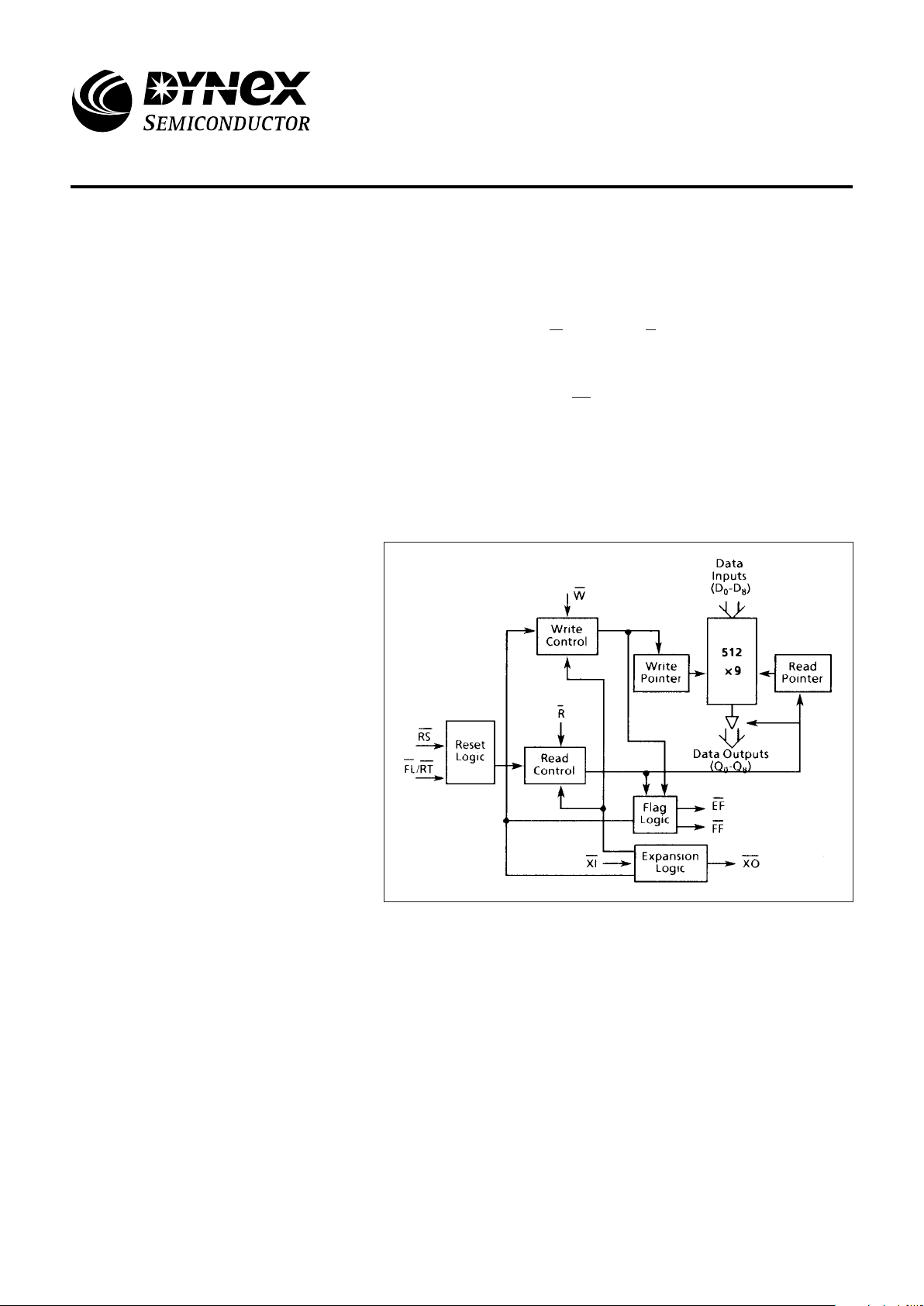
Figure 1: Block Diagram
MA7001
Radiation Hard 512x9 Bit FIFO
Replaces June 1999 version, DS3519-4.0 DS3519-5.0 January 2000
Page 2
MA7001
2/15
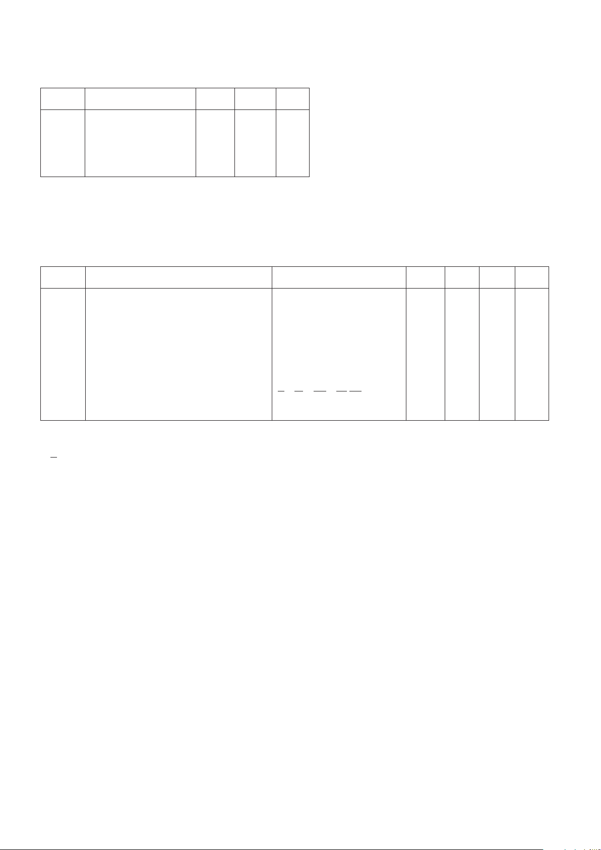
DC CHARACTERISTICS AND RATINGS
Symbol Parameter Min. Max. Units
V
DD
Supply Voltage -0.5 7.0 V
V
IN
Input Voltage -0.3 VDD+0.3 V
T
A
Operating Temperature -55 125 °C
T
S
Storage Temperature -65 150 °C
Stresses above those listed may cause permanent
damage to the device. This is a stress rating only and
functional operation of the device at these conditions, or at
any other condition above those indicated in the
operations section of this specification, is not Implied
Exposure to absolute maximum rating conditions for
extended periods may affect device reliability.
Figure 2: Absolute Maximum Ratings
The following D.C. and A.C. electrical characteristics apply to pre-radiation at TA = -55°C to +125°C, VDD = 5V ±10% and post
100kRad(Si) total dose radiation at TA = 25°C, VDD = 5V ±10%. GROUP A SUBGROUP 1, 2, 3.
Symbol Parameter Conditions Min. Typ. Max. Unit
V
IH
Input logic '1' voltage - 2.0 - - V
V
IL
Input logic '0' voltage - - - 0.8 V
I
IL
Input leakage current (any input) (Note 4) Note 1 -10 - 10 µA
I
OL
Output leakage current (Note 4) Note 2 -50 - 50 µA
V
OH
Output logic '1' voltage l
OUT
= -1mA 2.4 - - V
V
OL
Output loglc '0' voltage l
OUT
= 2mA - - 0.4 V
I
DD1
Average VDD power supply current (Note 3) Freq = 10MHz - 70 100 mA
I
DD2
Average standby current (Note 3) R = W = RS = FL/RT = VDD/2 - 8 15 mA
I
DD3(L)
Powerdown current (Note 3) All Inputs = VDD -0.2V - - 3.0 mA
NOTES:
1. Measurements with VSS ≤ VIN ≤ V
DD
2. R > VIH, VSS ≤ V
OUT
≤ V
DD
3. IDD measurements are made wlth outputs open, VDD = 5.5V
4. Guaranteed but not measured at -55°C
Figure 3a: DC Electrical Characteristics
Page 3

MA7001
3/15
AC CHARACTERISTICS
Characteristics apply to pre-radiation at TA = -55°C to +125°C, VDD = 5V ±10% and post
100kRad(Si) total dose radiation at TA = 25°C, VDD = 5V ±10%. GROUP A SUBGROUP 9, 10, 11.
Symbol Parameter Min. Max. Units
t
RC
Read Cycle Time 110 - ns
t
A
Access Time - 100 ns
t
RR
Read Recovery Time 25 - ns
t
RPW
Read Pulse Width (Note 2) 85 - ns
t
RLZ
Read Pulse Low to Data Bus at Low Z (Note 3) 10 - ns
t
DV
Data Valid from Read Pulse High 20 - ns
t
RHZ
Read Pulse High to Data Bus at High Z (Note 3) - 30 ns
t
WC
Write Cycle Time 100 - ns
t
WPW
Write Pulse Width (Note 2) 80 - ns
t
WR
Write Recovery Time 20 - ns
t
DS
Data Setup Time 40 - ns
t
DH
Data Hold Time 10 - ns
t
RSC
Reset Cycle Time (Note 3) 100 - ns
t
RS
Reset Pulse Width (Note 2) 80 - ns
t
RSR
Reset Recovery Time (Note 3) 20 - ns
t
RTC
Retransmit Cycle Time (Note 3) 100 - ns
t
RT
Retransmit Pulse Width (Note 2) 80 - ns
t
RTR
Retransmit Recovery Time (Note 3) 20 - ns
t
EFL
Reset to Empty Flag Low - 100 ns
t
REF
Read Low to Empty Flag Low - 90 ns
t
RFF
Read High to Full Flag High - 70 ns
t
WEF
Write High to Empty Flag High - 70 ns
t
WFF
Write Low to Full Flag Low - 90 ns
t
EFR
EF High to Valid Read (Note 3) 10 - ns
t
RPI
Read Protect Indeterminant (Note 3) - 35 ns
t
FFW
FF High to Valid Wrlte (Note 3) 10 - ns
t
WPI
Write Protect Indeterminant (Note 3) - 35 ns
Notes:
1. Timings referenced as in A.C. Test Conditions, figure 5
2. Pulse wldths less than minimum values are not allowed
3. Values guaranteed by deslgn, not currently tested
Figure 3b: AC Characteristics
Page 4

MA7001
4/15
Symbol Parameter Conditions
FT Functionality VDD = 3-6V, FREQ = 100kHz - 9MHz
VIL = VSS, VIH = VDD, VOL ≤ 1.5V, VOH ≥ 1.5V
TEMP = -55 to +125°C, RADIATION 1MRAD TOTAL DOSE
GROUP A SUBGROUPS 7, 8A, 8B
Figure 3b: Functionality
Subgroup Definition
1 Static characteristics specified in Table 3a at +25°C
2 Static characteristics specified in Table 3a at +125°C
3 Static characteristics specified in Table 3a at -55°C
7 Functional characteristics specified in Table 3c at +25°C
8A Functional characteristics specified in Table 3c at +125°C
8B Functional characteristics specified in Table 3c at -55°C
9 Switching characteristics specified in Table 3b at +25°C
10 Switching characteristics specified in Table 3b at +125°C
11 Switching characteristics specified in Table 3b at -55°C
Figure 4: Definition of Subgroups
Page 5
MA7001
5/15
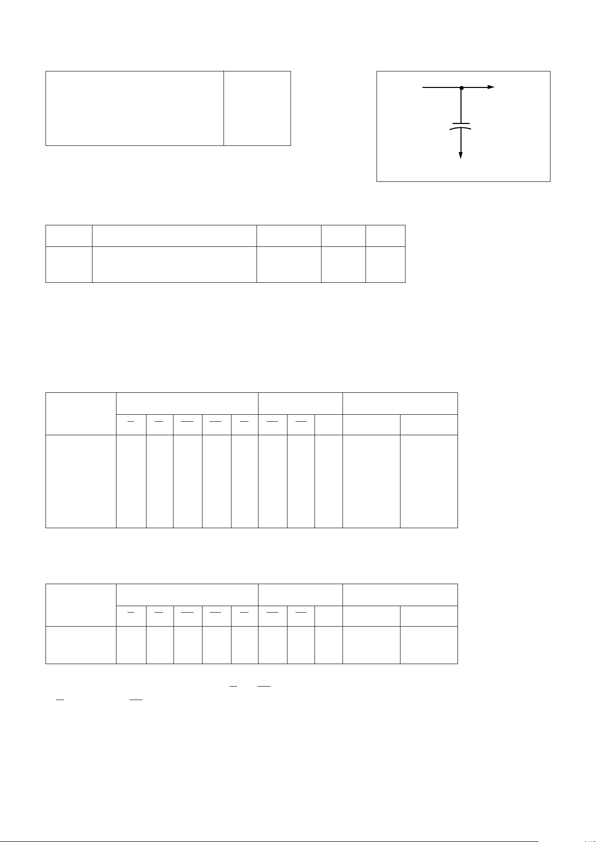
Input Pulse Levels GND to 3.0V
Input Rise and Fall Times 5ns
Input Timing Reference Levels 1.5V
Output Reference Levels 1.5V
Output Load See Figure 7
Figure 5: AC Test Conditions
Symbol Parameter Conditions Max. Unit
C
IN
Input Capacltance (Note 1) VIN = 0V 7 pF
C
OUT
Output Capacitance (Notes 1 and 2) V
OUT
= 0V 12 pF
NOTES:
1. Characterized values, not currently tested.
2. With output deselected.
Figure 6: Capacitance
TRUTH TABLES
Input Output Pointer
Operation
R W RS RT Xl EF FF Data Read Write
Reset 1 1 0 x 0 0 1 Z Zero Zero
Retransmit* 1110011Z Zero N/C
Read 1→0x11011valid Increment N/C
Read x x 11001Z N/C N/C
Write x 1→0 1 1 0 x 1 x N/C Increment
Write x x 11010x N/C N/C
* Only available if less than 512 writes since last reset.
Figure 8: Single Device or Width Expansion: Read, Write, Reset and Retransmit
Input Output Pointer
Operation
R W RS FL Xl EF FF Data Read Write
Reset First 1100101Z Zero Zero
Reset Rest 1101101Z Zero Zero
NOTES:
1. See Modes of Operation for connections of
Xl and XO in depth expansion mode.
2. XI is connected to XO of previous device (Figure 12).
Figure 9: Depth Expansion: Reset and First Load
Output
under test
Test Point
LOAD 1
≤50pF*
Figure 7: Output Load
* Includes jig
and scope
capacitances
Page 6

MA7001
6/15
SIGNAL DESCRIPTIONS
Reset (RS)
Reset occurs when RS is in a low state, setting both read and
write pointers to the first location in memory. Reset is required
prior to the first write. Both READ (R) and WRITE (W) signals
must be in high states during reset.
Read Enable (R):
Providing the EMPTY FLAG (EF) is not set, i.e. there is still
data to be read, a read cycle commences on the falling edge of
R, (see Figure 16). Data is read in a First-ln First-Out manner
independent of write operations. When reads are disabled
data outputs (Q0 - Q8) are in a high impedance state. Reading
the last available memory location sets the EMPTY FLAG
(EF), which is cleared following a write cycle.
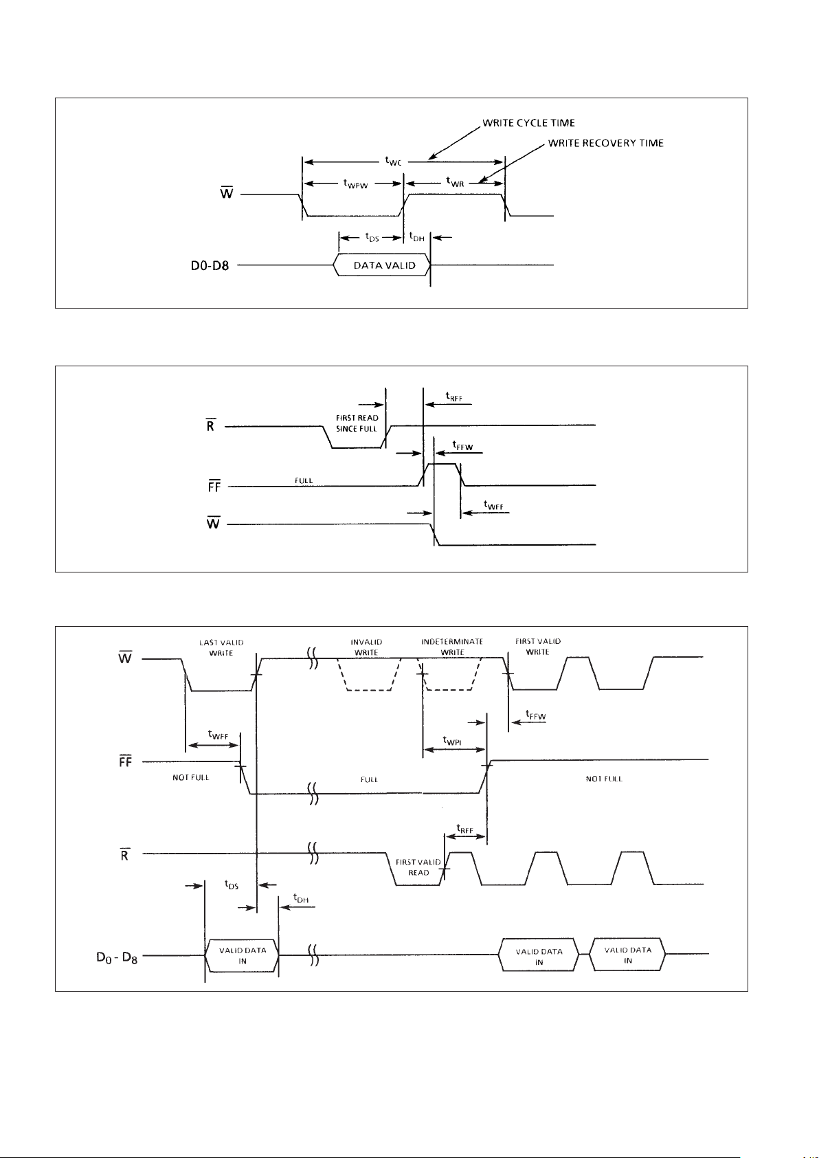
Write Enable (W):
Providing the FULL FLAG (FF) is not set, i.e. there exists at
least one memory location for writing, a write cycle
commences on the falling edge of (W), (see Figure 17). Data is
written into consecutive memory locations independent of read
operations on the rising edge of W. Data set up and hold times
are with respect to the rising edge of W.
Expansion In (Xl):
There are two possible modes of operation for the FIFO. One
with Xl grounded in which the device is in singledevice mode,
the other is a depth expension mode or daisy chain
configuration. In the latter mode Xl inputs come from
EXPANSION OUT (XO) outputs of the device preceding it in
the chain.
Expansion Out (XO):
In depth expansion mode XO from one device signals the next
device in the chain that the last location in its memory has been
accessed.
Full Flag (FF):
FF becomes active when the last available memory location
has been written to, (see Figure 18). In general, this occurs
whenever the write pointer coincides with the read pointer
following a write cycle. Writes are inhibited while FF is active,
and may only proceed after a read cycle has occured.
FF will go high t
RFF
after completion of a valid READ operation.
FF will go low t
WFF
from the beginning of a subsequent WRITE
operation, provided that a second READ has not been
completed. Writes beginning t
FFW
after FF goes high, are valid.
Writes beginning after FF goes low and ending more than t
WPI
before FF goes high, are invalid (ignored). Writes beginning
less than twpl before FF goes high and less than t
FFW
later,
may or may not occur (be valid) depending on the internal flag
status (see Figure 19).
If a Write to the last but one physical location completes while
the last location (511th) is being Read, the FF will not be
activated. The next Read should start after the last Write has
completed.
As a WRITE operation is being performed to the last physical
memory location (511th) whilst the READ pointer is waiting at
the 510th physical location the FULL flag is activated for a
duration less than 20ns.
Note: The last physical location (511th) is accessed after 511
WRITE or READ operations after RESET.
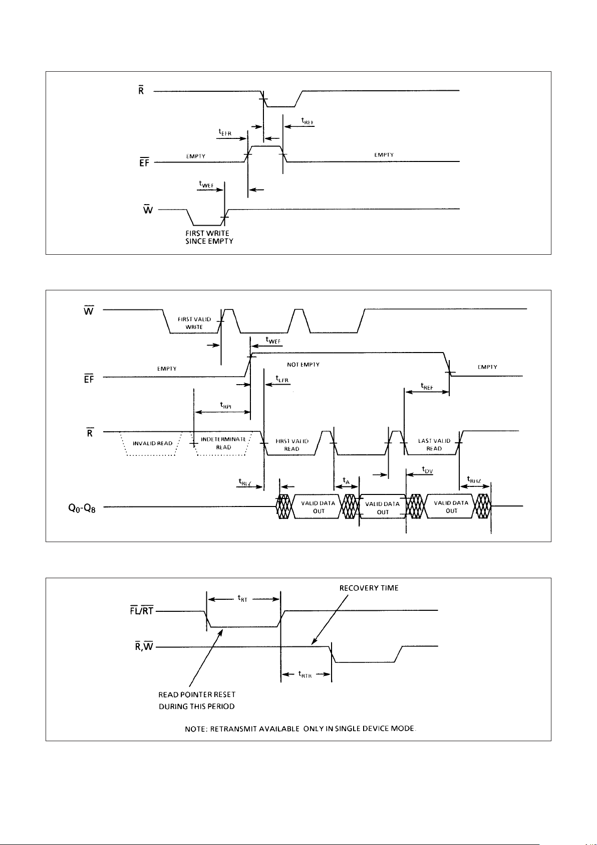
Empty Flag (EF):
Following an initial RESET EF is active, becoming inactive
after the first write cycle, (see Figure 20). EF becomes active
once the read and write pointers are coincident following a
read cycle. Reading will not take place whilst EF is active, and
may only proceed once a write cycle has occured.
EF will go high t
WEF
after completion of a valid WRITE
operation. EF will again go low t
REF
from the beginning of a
subsequent READ operation, provided that a second WRITE
has not been completed. Reads beginning t
EFR
after EF goes
high, are valid. Reads begun after EF goes low and ending
more than t
RPI
before EF goes high, are invalid (ignored).
Reads beginning less than t
RIP
before EF goes high and less
than t
EFR
later, may or may not occur (be valid) depending on
the internal flag status (See Figure 21). If a Read to the last but
one physical location completes while the last location (511th)
is being written, the EF will not be activated. The next Read
should be activated after the last Write has completed.
First Load/Retransmit (FL/RT):
This is a dual purpose input depending on the mode of
operation of the device. In single device mode Xl = 0 data may
be retransmitted, i.e. it may be re-read. In depth expansion
mode FL signifies the first device in the chain. When RT is
pulsed low the read pointer is set to the first memory location.
The write pointer is unaffected. This feature is disabled in
depth expansion mode, and can only be applied when R and
W are inactive (See Figure 22).
Data Inputs (D0 - D8): Data inputs, 9 bit word, for write
operations.
Data Outputs (Q0 - Q8):
Data outputs, 9 bit word, for read operations. When R is
inactive these outputs are in a high impedance state.
Page 7
MA7001
7/15
MODES OF OPERATION
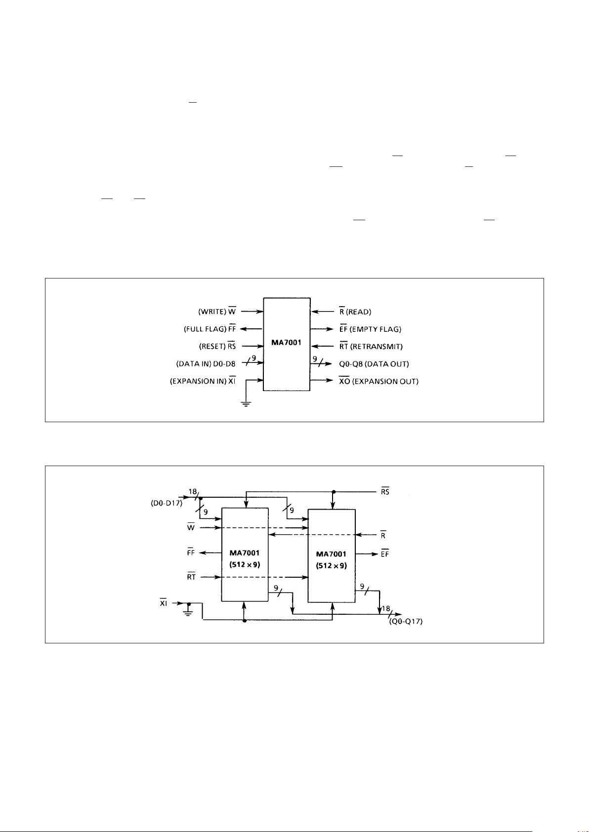
Single Device Mode:
The single device mode is used with Xl grounded. (See Figure
10). In this mode the retransmit facility may be used to re-read
the data when less than 512 have been performed between
resets.
Width Expansion Mode:
In this mode two or more devices are used, depending on the
word length required, with the same control inputs applied to
each. The same operations are applied to all devices, thus
warning flags EF and FF are available from any or all of the
devices. Output Signals from devices in this mode should not
be merged. Figure 11 illustrates two devices configured in
width expansion mode to give an 18 bitword, (512 x 18).
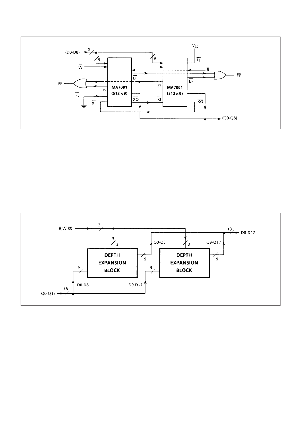
Depth Expansion Mode:
This has applications where more than 512 words are
required. The RETRANSMIT facility is not available in this
mode.
Two or more devices are organised in a daisy chain. The first
device in the chain has FL grounded, all others have FL in high
states. XO of each device is connected to XI of the next device
in the chain.
The same read, write and reset signals are applied to each
device. External logic is required to form new empty and full
flags, i.e. all EF’s are ORed together and all FF’s are ORed
together to form new empty and full flags respectively.
Figure 12 illustrates depth expansion of 2 devices (1024 x 9).
Figure 10: Single Device Mode (512 x 9 bits)
Figure 11: Width Expansion Mode (512 x 18 bits)
Page 8
MA7001
8/15
Figure 12: Depth Expansion Mode (1024 x 9 bits)
Compound Expansion Mode:
Both width and depth expansion can be implemented into the
same expansion block. Note that no control signals are in
conflict in either of the two expansion modes, i.e. width or
depth expansion modes. Utilising compound expansion large
FIFO arrays are possible. Figure 13 illustrates the use of
compound expansion.
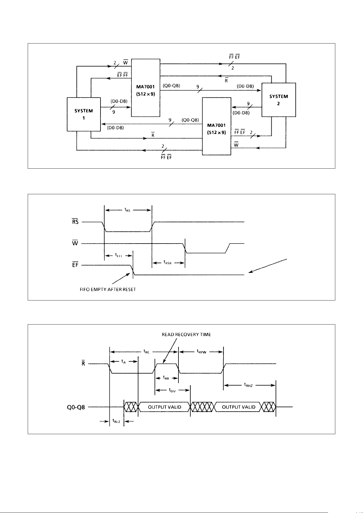
Bidirectional Mode:
The FIFO is a unidirectional device, i.e. one system reads,
another writes. In cases where full communication is required
between two or more systems, two or more groups of devices
can be used. These groups can utilise any or all of the
expansion modes already mentioned. Figure 14 illustrates 2
systems connected so that each can transmit data to and
recieve data from each other, (see Modes of Operation for
connection of control and data signals).
Figure 13: Compound Expansion
Page 9
MA7001
9/15
Figure 14: Bidirectional Mode (512 x 9 bits each way)
Figure 15: Reset
Figure 16: Asynchronous Read
EMPTY FLAG
GOES 'HIGH'
AFTER WRITE
(See Figure 20)
Page 10
MA7001
10/15
Figure 17: Asynchronous Write
Figure 18: Read/Write to Full Flag
Figure 19: Write and Full Flag
Page 11
MA7001
11/15
Figure 20: Write/Read to Empty Flag
Figure 21: Read and Empty Flag
Figure 22: Retransmit Timing
Page 12
MA7001
12/15
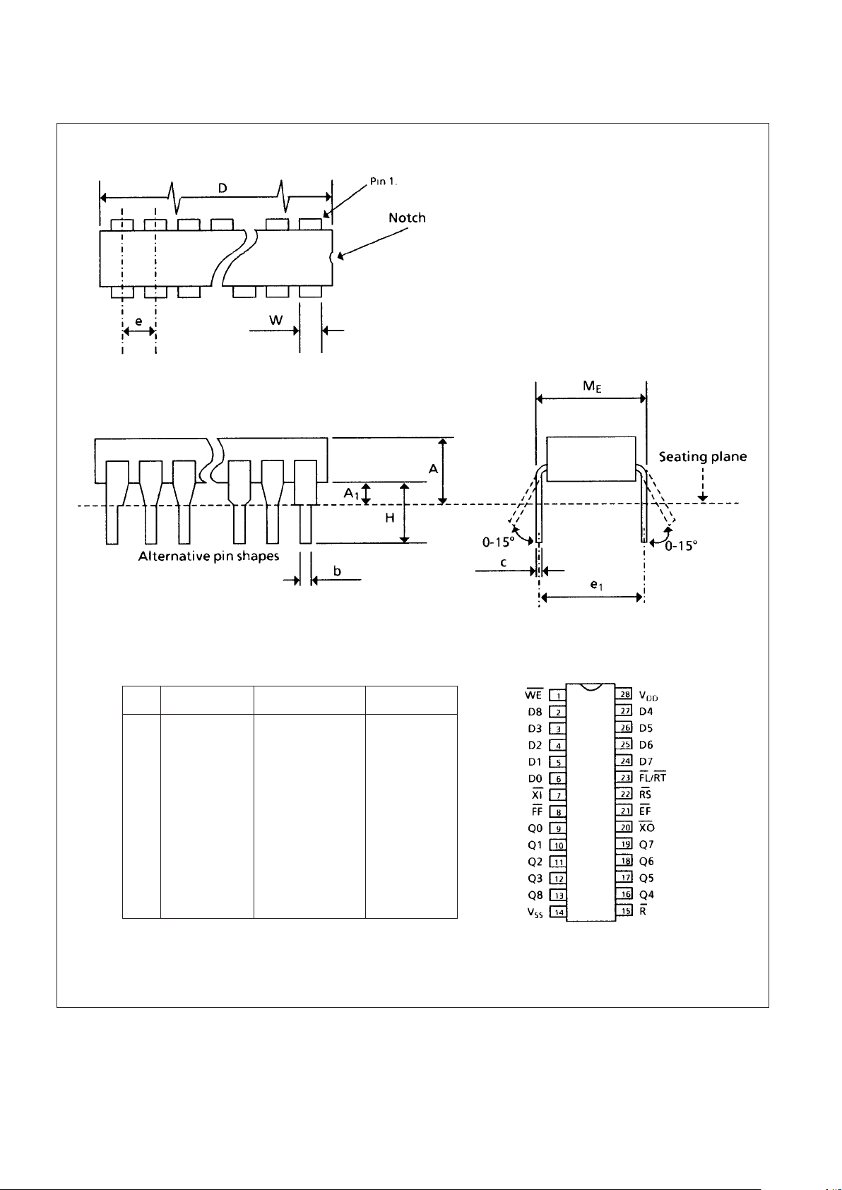
OUTLINES AND PIN ASSIGNMENTS
Figure 23: 28 Lead Ceramic DIL (Solder Seal) - Package Style C
Ref. Min. Nom. Max.
A - - 5.71 (0.225)
A
1
0.38 (0.015) - 1.53 (0.060)
b 0.35 (0.014) - 0.59 (0.023)
c 0.20 (0.008) - 0.36 (0.014)
D - - 36.02 (1.418)
e - 2.54 (0.100) typ. e
1
- 15.24 (0.600) typ. H 4.71 (0.185) - 5.38 (0.212)
M
E
- - 15.90 (0.626)
W - - 1.53 (0.060)
Dimensions in mm (inches)
Page 13
MA7001
13/15
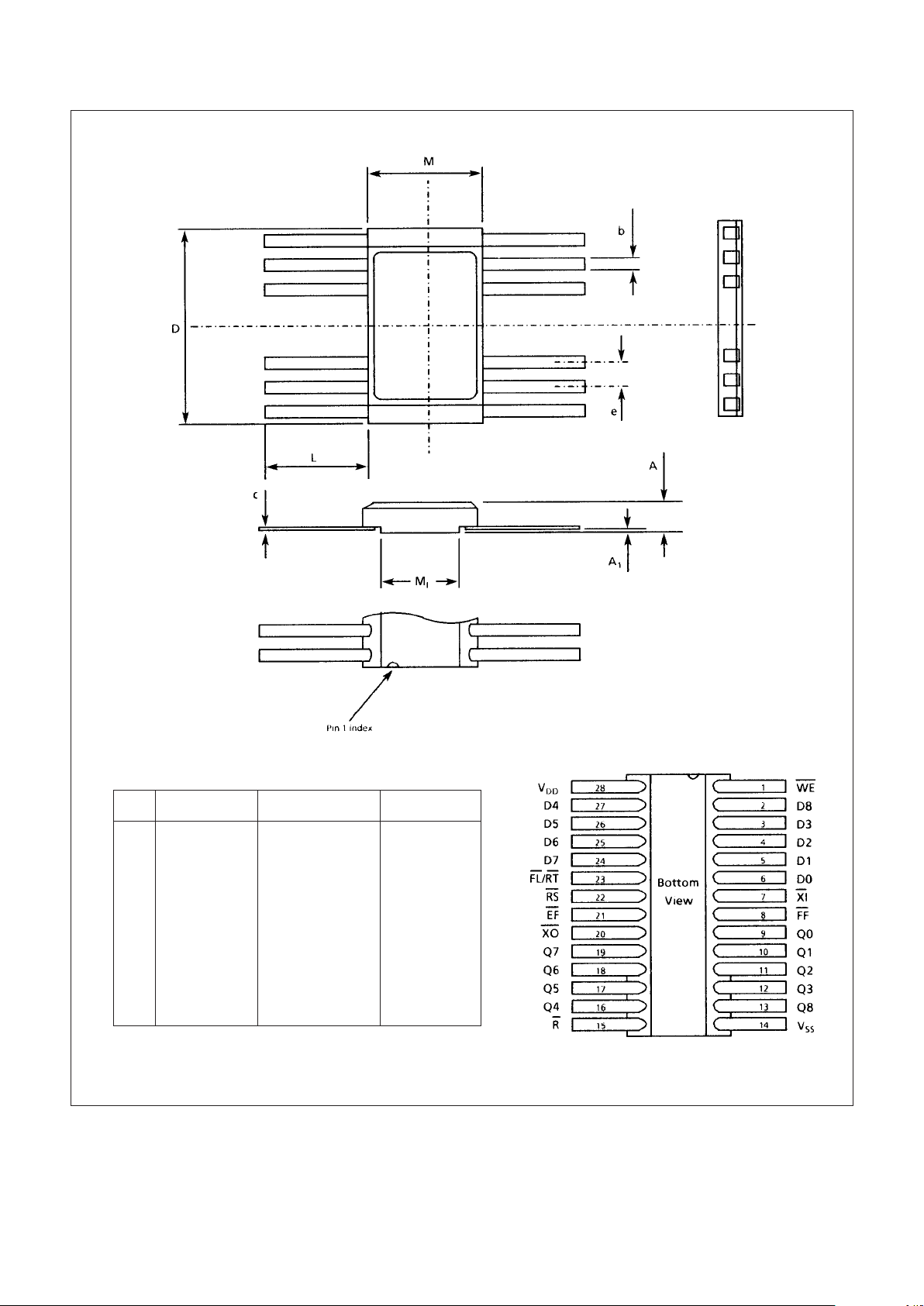
Figure 24: 28 Lead Ceramic Flatpack (Solder Seal) - Package Style F
Ref. Min. Nom. Max.
A - - 2.97 (0.117)
A
1
(0.026) - b (0.015) - 0.48 (0.019)
c 0.10 (0.003) - 0.15 (0.006)
D 18.08 (0.712) - 18.49 (0.728)
e - 1.27 (0.050) typ. L (0.315) - (0.365)
M 12.50 (0.492) - 12.09 (0.508)
M1 (0.372) - (0.388)
Dimensions in mm (inches)
Page 14

MA7001
14/15
RADIATION TOLERANCE
Total Dose Radiation Testing
For product procured to guaranteed total dose radiation
levels, each wafer lot will be approved when all sample
devices from each lot pass the total dose radiation test.
The sample devices will be subjected to the total dose
radiation level (Cobalt-60 Source), defined by the ordering
code, and must continue to meet the electrical parameters
specified in the data sheet. Electrical tests, pre and post
irradiation, will be read and recorded.
GEC Plessey Semiconductors can provide radiation
testing compliant with MIL-STD-883 test method 1019,
Ionizing Radiation (Total Dose).
Total Dose (Function to specification)* 1x10⁵ Rad(Si)
Transient Upset (Stored data loss) 5x10¹⁰ Rad(Si)/sec
Transient Upset (Survivability) >1x10
12
Rad(Si)/sec
Neutron Hardness (Function to specification) >1x10¹⁵ n/cm
2
Single Event Upset** 3.4x10⁻⁹ Errors/bit day
Latch Up Not possible
* Other total dose radiation levels available on request
** Worst case galactic cosmic ray upset - interplanetary/high altitude orbit
Figure 25: Radiation Hardness Parameters
Page 15
MA7001
15/15
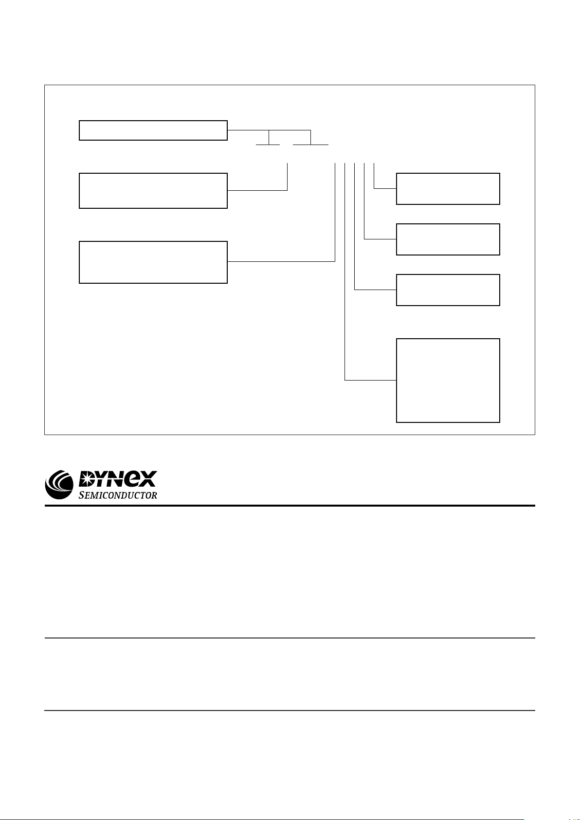
ORDERING INFORMATION
For details of reliability, QA/QC, test and assembly
options, see ‘Manufacturing Capability and Quality
Assurance Standards’ Section 9.
Unique Circuit Designator
SRRadiation Hard Processing
100 kRads (Si) Guaranteed
Radiation Tolerance
C
F
N
Ceramic DIL (Solder Seal)
Flatpack (Solder Seal)
Naked Die
Package Type
QA/QCI Process
(See Section 9 Part 4)
Test Process
(See Section 9 Part 3)
Assembly Process
(See Section 9 Part 2)
L
C
D
E
B
S
Rel 0
Rel 1
Rel 2
Rel 3/4/5/STACK
Class B
Class S
Reliability Level
MAx7001xxxxx
CUSTOMER SERVICE CENTRES
France, Benelux, Italy and Spain Tel: +33 (0)1 69 18 90 00. Fax: +33 (0)1 64 46 54 50
North America Tel: 011-800-5554-5554. Fax: 011-800-5444-5444
UK, Germany, Scandinavia & Rest Of World Tel: +44 (0)1522 500500. Fax: +44 (0)1522 500020
SALES OFFICES
France, Benelux, Italy and Spain Tel: +33 (0)1 69 18 90 00. Fax: +33 (0)1 64 46 54 50
Germany Tel: 07351 827723
North America Tel: (613) 723-7035. Fax: (613) 723-1518. Toll Free: 1.888.33.DYNEX (39639) /
Tel: (831) 440-1988. Fax: (831) 440-1989 / Tel: (949) 733-3005. Fax: (949) 733-2986.
UK, Germany, Scandinavia & Rest Of World Tel: +44 (0)1522 500500. Fax: +44 (0)1522 500020
These offices are supported by Representatives and Distributors in many countries world-wide.
© Dynex Semiconductor 2000 Publication No. DS3518-5 Issue No. 5.0 January 2000
TECHNICAL DOCUMENTATION – NOT FOR RESALE. PRINTED IN UNITED KINGDOM
HEADQUARTERS OPERATIONS
DYNEX SEMICONDUCTOR LTD
Doddington Road, Lincoln.
Lincolnshire. LN6 3LF. United Kingdom.
Tel: 00-44-(0)1522-500500
Fax: 00-44-(0)1522-500550
DYNEX POWER INC.
Unit 7 - 58 Antares Drive,
Nepean, Ontario, Canada K2E 7W6.
Tel: 613.723.7035
Fax: 613.723.1518
Toll Free: 1.888.33.DYNEX (39639)
This publication is issued to provide information only which (unless agreed by the Company in writing) may not be used, applied or reproduced for any purpose nor form part of any order or contract nor to be regarded
as a representation relating to the products or services concerned. No warranty or guarantee express or implied is made regarding the capability, performance or suitability of any product or service. The Company
reserves the right to alter without prior notice the specification, design or price of any product or service. Information concerning possible methods of use is provided as a guide only and does not constitute any
guarantee that such methods of use will be satisfactory in a specific piece of equipment. It is the user's responsibility to fully determine the performance and suitability of any equipment using such information and
to ensure that any publication or data used is up to date and has not been superseded. These products are not suitable for use in any medical products whose failure to perform may result in significant injury
or death to the user. All products and materials are sold and services provided subject to the Company's conditions of sale, which are available on request.
All brand names and product names used in this publication are trademarks, registered trademarks or trade names of their respective owners.
http://www.dynexsemi.com
e-mail: [email protected]
Datasheet Annotations:
Dynex Semiconductor annotate datasheets in the top right hard corner of the front page, to indicate product status. The annotations are as follows:-
T arget Information: This is the most tentative form of information and represents a very preliminary specification. No actual design work on the product has been started.
Preliminary Information: The product is in design and development. The datasheet represents the product as it is understood but details may change.
Advance Information: The product design is complete and final characterisation for volume production is well in hand.
No Annotation: The product parameters are fixed and the product is available to datasheet specification.
 Loading...