

Page 1
MAS 35x9F
MPEG Layer 2/3,
AAC Audio Decoder,
G.729 Annex A Codec
Edition October 31, 2000
6251-505-2AI
ADVANCE INFORMATION
MICRONAS
MICRONAS
Page 2

MAS 35x9F ADVANCE INFORMATION
Contents
Page Section Title
5 1. Introduction
5 1.1. Features
6 1.2. Features of the MAS 35x9F Family
7 1.3. Application Overview
8 2. Functional Description of the MAS 35x9F
82.1.Overview
8 2.2. Architecture of the MAS 35x9F
8 2.3. DSP Core
8 2.3.1. RAM and Registers
9 2.3.2. Firmware and Software
9 2.3.2.1. Internal Program ROM and Firmware, MPEG-Decoding
9 2.3.2.2. Program Download Feature
9 2.4. A udio Codec
9 2.4.1. A/D Converter and Microphone Amplifier
9 2.4.2. Baseband Processing
9 2.4.2.1. Bass, Treble, and Loudness
9 2.4.2.2. Micronas Dynamic Bass (MDB)
10 2.4.2.3. Automatic Volume Control (AVC)
10 2.4.2.4. Balance and volume
10 2.4.3. D/A Converters
10 2.4.4. Output Amplifiers
11 2.5. Clock Management
11 2.5.1. DSP Clock
11 2.5.2. Clock Output At CLKO
11 2.6. Power Supply Concept
11 2.6.1. Power Supply Regions
12 2.6.2. DC/DC Converters
12 2.6.3. Power Supply Configurations
14 2.7. Battery Voltage Supervision
15 2.8. Interfaces
15 2.8.1. I2C Control Interface
15 2.8.2. SPDIF Input Interface
15 2.8.3. S/PDIF Output
15 2.8.4. Multiline Serial Audio Input (SDI, SDIB)
15 2.8.5. Multiline Serial Output (SDO)
15 2.8.6. Parallel Input/Output Interface (PIO)
16 2.9. MPEG Synchronization Output
16 2.10. Default Operation
16 2.10.1. Stand-by Functions
16 2.10.2. Power-Up of the DC/DC Converters and Reset
17 2.10.3. Control of the Signal Processing
17 2.10.4. Start-up of the Audio Codec
17 2.10.5. Power-Down
2 Micronas
Page 3

ADVANCE INFORMATION
Contents, continued
Page Section Title
18 3. I2C Interface
18 3.1. General
18 3.1.1. Device Address
18 3.1.2. I2C Registers and Subaddresses
19 3.1.3. Naming Convention
20 3.2. Direct Configuration Registers
20 3.2.1. Write Direct Configuration Registers
20 3.2.2. Read Direct Configuration Register
25 3.3. DSP Core
25 3.3.1. Access Protocol
26 3.3.1.1. Run and Freeze
26 3.3.1.2. Read Register (Code Ahex)
26 3.3.1.3. Write Register (Code Bhex)
26 3.3.1.4. Read D0 Memory (Code Chex)
27 3.3.1.5. Short Read D0 Memory (Code C4hex)
27 3.3.1.6. Read D1 Memory (Code Dhex)
27 3.3.1.7. Short Read D1 Memory (Code D4hex)
27 3.3.1.8. Write D0 Memory (Code Ehex)
28 3.3.1.9. Short Write D0 Memory (Code E4hex)
28 3.3.1.10. Write D1 Memory (Code Fhex)
28 3.3.1.11. Short Write D1 Memory (Code F4hex)
28 3.3.1.12. Clear SYNC Signal (Code 5hex)
28 3.3.1.13. Default Read
29 3.3.1.14. Fast Program Download
29 3.3.1.15. Serial Program Download
29 3.3.2. List of DSP Registers
30 3.3.3. List of DSP Memory Cells
30 3.3.3.1. Application Select and Running
30 3.3.3.2. Application Specific Control
40 3.3.4. Ancillary Data
40 3.3.5. DSP Volume Control
41 3.3.6. Explanation of the G.729 Data Format
41 3.4. Audio Codec Access Protocol
41 3.4.1. Write Codec Register
41 3.4.2. Read Codec Register
42 3.4.3. Codec Registers
49 3.4.4. Basic MDB Configuration
MAS 35x9F
50 4. Specifications
50 4.1. Outline Dimensions
51 4.2. Pin Connections and Short Descriptions
53 4.3. Pin Descriptions
53 4.3.1. Power Supply Pins
53 4.3.2. Analog Reference Pins
53 4.3.3. DC/DC Converters and Battery Voltage Supervision
54 4.3.4. Oscillator Pins and Clocking
54 4.3.5. Control Lines
Micronas 3
Page 4

MAS 35x9F ADVANCE INFORMATION
Contents, continued
Page Section Title
54 4.3.6. Parallel Interface Lines
54 4.3.6.1. PIO Handshake Lines
54 4.3.7. Serial Input Interface (SDI)
54 4.3.8. Serial Input Interface B (SDIB)
54 4.3.9. Serial Output Interface (SDO)
54 4.3.10. S/PDIF Input Interface
55 4.3.11. S/PDIF Output Interface
55 4.3.12. Analog Input Interfaces
55 4.3.13. Analog Output Interfaces
55 4.3.14. Miscellaneous
56 4.4. Pin Configurations
58 4.5. Internal Pin Circuits
60 4.6. Electrical Characteristics
60 4.6.1. Absolute Maximum Ratings
61 4.6.2. Recommended Operating Conditions
64 4.6.3. Digital Characteristics
2
65 4.6.3.1. I
66 4.6.3.2. Serial (I
68 4.6.3.3. Serial Output Interface Characteristics (SDO)
70 4.6.3.4. S/PDIF Input Characteristics
71 4.6.3.5. S/PDIF Output Characteristics
72 4.6.3.6. PIO As Parallel Input Interface: Demand Mode
73 4.6.3.7. PIO as Parallel Output Interface
74 4.6.4. Analog Characteristics
77 4.6.5. DC/DC Converter Characteristics
78 4.6.6. Typical Performance Characteristics
80 4.7. Typical Application in a Portable Player
81 4.8. Recommended DC/DC Converter Application Circuit
C Characteristics
2
S) Input Interface Characteristics (SDI, SDIB)
82 5. Data Sheet History
License Notice
Supply of this implementation of AAC technology does not convey a license nor imply any right to use this implementation in any finished end-user or ready-to-use final product. An independant license for such use is required.
contact: aacla@dolby.com
4 Micronas
Page 5

ADVANCE INFORMATION MAS 35x9F
MPEG Layer 2/3, AAC Audio Decoder,
G.729 Annex A Codec
Release Note: Revision bars indicate significant
changes to the previous edition. This data sheet
applies to MAS 35x9F version A2 .
1. Introduction
The MAS 35x9F is a single-chip, low-power MPEG
layer 2/3 and MPEG2-AAC audio stereo decoder. It
also contains the G.729 Annex A speech co mpress ion
and decompression technology for use in memorybased or broadcas t applica tions. Additiona l function ality is achievable via download software (e.g. CELP
voice decoder, Micronas SC4 (ADPCM) encoder /
decoder)
The MAS 35x 9F decoding block accepts compressed
digital da t a str e ams as serial bits tr ea m s , or pa rallel format and provides serial PCM and/or S/PD IF output
of decompressed au dio. In addition to the signal processing function the IC incorporates a high-performance stereo D/A co nverter, headphone amplifiers, a
stereo A/D converte r, a microphone amplifier, and two
DC/DC converters.
1.1. Features Firmware
– MPEG 1/2 layer 2 and layer 3 decoder
– Extension to MPEG 2 layer 3 for low bit rates
(“MPEG 2.5”)
– Extraction of MPEG Ancillary Data
–MPEG 2 AAC
2)
decoder (low complexity profile)
– Master or slave clock operation
– Adaptive bit rates (bit rate switching)
– Intelligent power management (processor clock is
dependent on sampling frequencies)
– Micronas G.729 Annex A speech compression and
decompression
– SDMI-compliant security technology
1)
– Stereo channel mixer
– Bass, treble and loudness function
– Micronas Dynamic Bass (MDB)
– Automatic Volume Control (AVC)
Thus, the MAS 35x9F provides a true ’ALL-IN-ONE’
solution that is ideally suited for highly optimized memory based portable music players with integrated
speech decoding function.
In MPEG 1 (IS O 11172-3), three hierarchical layers of
compression have been standardized. The most
sophisticated and complex, layer 3, allows compression rates of approximately 12:1 for mono and stereo
signals while still maintaining CD audio quality. Layer 2
(widely used in e.g. in DVD) achieves a compression of
8:1 without significant losses in audio quality.
The MAS 35x9F supports the ’Advanced Audio Coding’ (AAC) that is also defined as aprt of MPEG 2. AAC
provides compression rates up to 16:1. MPEG 2
defines several profiles for different applications. This
IC decodes the ’low complexity profile’ that is especially optimized for portable applications.
The MAS 35x9 F also imp lement s a voice encoder and
decoder that is c ompliant to the ITU Standard G.7 29
Annex A.
SC4 is a propr ietary Mic ronas speech codec technology that can be downloaded to the MAS 35x9F to
allow recording and playing back speech at various
sampling rates.
Interfaces
– 2 serial asynchronous interfaces for bitstreams and
uncompressed digital audio
– Parallel handshake bit stream input
2
– Serial audio output via I
S and related formats
– S/PDIF data input and output
2
– Controlling via I
C interface
Hardware Features
– Two independent embedded DC/DC converters
(e.g. for DSP and flash RAM supply)
– Low DC/DC converter start-up voltage (0.9 V)
– DC converter efficiency up to 95 %
– Battery voltage monitor
– Low supply voltage (down to 2.2 V)
– Low power dissipation (<70 mW)
– High-performance RISC DSP core
– On-chip crystal oscillator
– Hardware power management and power-off func-
tions
– Microphone amplifier
– Stereo A/D converter for FM/AM-radio and speech
input
– CD quality stereo D/A converter
– Headphone amplifier
Micronas 5
Page 6
MAS 35x9F ADVANCE INFORMATION
– Noise and power-optimized volume
– External clock or crystal frequency of 13...20 MHz
1)
Not yet supported in version A2
2)
See License Note on page 4
– Standby current < 10 µA
1.2. Features of the MAS 35x9F Family
Feature 3509 3519 3529 3539 3549 3559
Layer 3 Decoder XXXX
G.729 Encoder/Decoder X X X
AAC Decoder XX X
6 Micronas
Page 7
ADVANCE INFORMATION MAS 35x9F
1.3. Application Overview
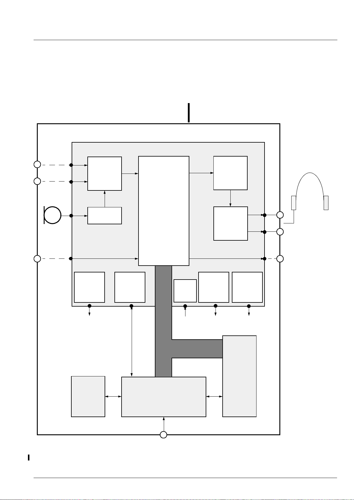
The following block diagram shows an example appl ication for the MAS 35x9F in a portable audio player
device. Besides a simple controller and the external
flash memories, all required components are integrated in the MAS 35x9F. The MAS 35x9F supports
both speech and ra dio quality audio enco ding, as well
as compressed-audio decoding tasks.
Portable Digital Music Player
MAS 35x9F
optional
line in
optional
digital in
S/PDIF
or
serial
Microphone
amplifier
Crystal
Osc./PLL
A/D
2
C DC/DC2
Audio
baseband
features
DSP Core
MP3
AAC
G.729
Optional
Software
Downloads
Battery
Voltage
Monitor
Fig. 1–1 depicts a portable audio application that is
power optimized. The two embedde d DC/DC converters of the MAS 35x9F generate optimum power supply
voltages for the DSP core and also for state-of-the art
flash memories that typically require 2.7 to 3.3 V supply.
The performance of the DC/DC converters reaches
efficiencies up to 95 %.
D/A
Headphone
amplifier
Volume
DC/DC1I
Headphone
digital out
S/PDIF or serial
System clock e.g. 2.2 V e.g. 3.0 V
C Control
2
I
Display
Keyboard
Fig. 1–1: Example application for the MAS 35x9F in a portable audio player device
Micronas 7
Parallel I/O Bus
PC Connector
C
µ
e.g. 1.0 V
I2C
Flash RAM
Page 8
MAS 35x9F ADVANCE INFORMATION
2. Functional Description of the MAS 35x9F
2.1. Overview
The MAS 35x9F is intended for use in portable consumer audio applications. It receives S/PDIF, parallel
or serial data streams and decodes MPEG Layer 2
and 3 (including the low sampling frequency extensions) and MPEG 2 AAC. In addition, special downloadable software expands the function to a low-bitrate
CELP codec for speech recording. Other download
options (SDMI, other audio encoders/decoders) are
available on request. Compressed speech data may
be stored in an external memory via the parallel port.
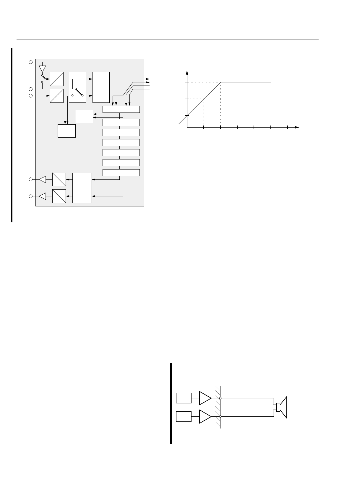
2.2. Architecture of the MAS 35x9F
The hardware of the MAS 35x9F consists of a highperformance RISC Digital Signal Processor (DSP),
Mic. Input
(incl. Bias)
Audio Codec
Line Input
1
2
A/D
and appropriate interfaces. A hardware overview of the
IC is shown in Fig. 2–1.
2.3. DSP Core
The internal processor is a dedicated DSP for
advanced audio applications.
2.3.1. RAM and Registers
The DSP core has access to two RAM banks de noted
D0 and D1. All RAM a ddresses can be accessed in a
20-bit or a 16-bit mode via I
2
C bus. For fast access of
internal DSP states the processor core has an address
space of 256 data regi ste rs which can be acce ss ed by
2
C bus. For more details please refer to Section 3.3.
I
on page 25.
2
MIX
Audio
Proc.
D/A
Audio
2
Output
S/PDIF Input 1
S/PDIF Input 2
Serial Audio
(I2S, SDI)
Serial Audio
(stream, SD IB)
V
BAT
V1
V2
Xtal
18.432 MHz
Volt.
Mon.
DC/DC 2 DC/DC 1
Div.
DSP Core
ALU MAC
Accumulators
Input Select
D0 D1
PLL
Synth.
ROM
Registers
Div.
Synthesizer
Clock
Serial
Audio
(I2S, SDO)
S/PDIF
Output
Control
Output Select
DCFR
DCCF
2
C
I
Interface
2
I
C
control
DSP
Codec
Parallel
I/O Bus
(PIO)
CLKO
ScalerOsc.
2
÷
Fig. 2–1: The MAS 35x9F architecture
8 Micronas
Page 9

ADVANCE INFORMATION MAS 35x9F
2.3.2. Firmware and Software
2.3.2.1. Internal Program ROM and Firmware,
MPEG-Decoding
The firmware im pleme nted in the pr ogram ROM of the
MAS 35x9F provides MPEG 1/2 Layer 2, MPEG 1/2
Layer 3 and MPEG 2 AAC-decoding as well as a
G.729 encoder and decoder.
The DSP operating sy stem starts the firmware in the
“Application Selecti on Mode”. By setting the appro priate bit in the Application Select memory cell (see
Tab le3–6 on page 31) the MPEG audio deco der or the
G.729 Codec can be activated.
The MPEG decoder provides an automatic standard
detection mode. If all MPEG audio decoders are
selected, the Layer 2, Layer 3 or AAC bitstream is re cognized and decoded automatically.
To add/remove MPEG layers while running in MPEG
decoding mode (e.g. Layer 2, Layer 3 (0x0c) to
Layer 2, Layer 3, AAC (0x1c)), the application selection has to be reset before writing the new value.
For general control purposes, the operation system
provides a set of I
2
C instructions that give access to
internal DSP registers and memory areas.
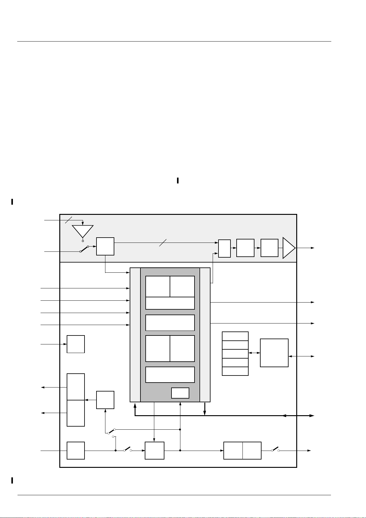
2.4. Audio Codec
A sophisticated set of audio converters and sound features has been implemented to comply with various
kinds of operating environ ments t hat range up to h ighend equipment (see Fig. 2–2 on page 10).
2.4.1. A/D Converter and Microphone Amplifier
A pair of A/D converters is provided for recording or
loop-through purposes. In addition, a microphone
amplifier inclu ding voltage supply function for an electret type microphone has been integrated.
2.4.2. Baseband Processing
The several baseband functions are applied to th e dig ital audio signal immediately before D/A conversion.
2.4.2.1. Bass, Treble, and Loudness
Standard baseband functions such as bass, treble,
and loudness are provided.
2.4.2.2. Micronas Dynamic Bass (MDB)
An auxiliar y digital volume control and mixer matrix is
applied to the digital stereo audio data. This ma trix is
capable of performing the balance control and a simple
kind of stereo basewidth enhanc ement. A ll four factors
LL, LR, RL, and RR are adjustable, please refer to Fig.
3–3 on page 40.
2.3.2.2. Program Download Feature
The standard functions of the MAS 35x9F can be
extended or substituted by downloading up to
4 kWords (1 Word = 20 bits) of program code and
additionally up to 4 kWords of coefficients into the
internal RAM .
The code must be downloaded by the
Download
command (see Section 3.3.1.14. on
Fast Program
page 29) into an area of RAM that is switchable from
Run
data memory to program memory. A
command
(see Section 3.3.1.1. on page 26) starts the operation.
The Micronas Dynamic Bass system (MDB) was
developed to extend the frequency range of loudspeakers or headphones below the cutoff frequen cy of
the speakers. In addit ion to dynamic ally ampl ifying the
low frequency bass signa ls, the MDB exploits the ps ychoacoustic phenomenon of the ‘missing fundamental’. Adding harmonics of the frequency components
below the cutoff frequency gives the impression of
actually hearing t he low frequency fundamental, while
at the same tim e retai ning t he loudne ss of t he or iginal
signal. Due to the parametric implementation of the
MDB, it can be customized to create different bass
effects and adapted to var ious loudsp eaker characteristics.
Micronas 9
Page 10
MAS 35x9F ADVANCE INFORMATION
Mic-In
A
D
A
D
Line-In
Deemphasis
Mono
50µs / 75µs
Mixer
Mono/Stereo
AVC
Bass/Treble
Loudness
Right invert
A
D
A
D
Volume
Balance
Audio
Codec
Mic-Amplifier incl. Bias
DSP
Output
MDB
Headphone
Amplifier
Q-peak
Q-peak
output level
dBr
9
−
15
−
21
−
30
−
24
−
Fig. 2–3: Simplified AVC characteristics
2.4.2.4. Balance and volume
18−12
−
6
−
6
+
0
input level
dBr
To minimize quantization nois e, the main volume control is automatically split into a digital and an analog
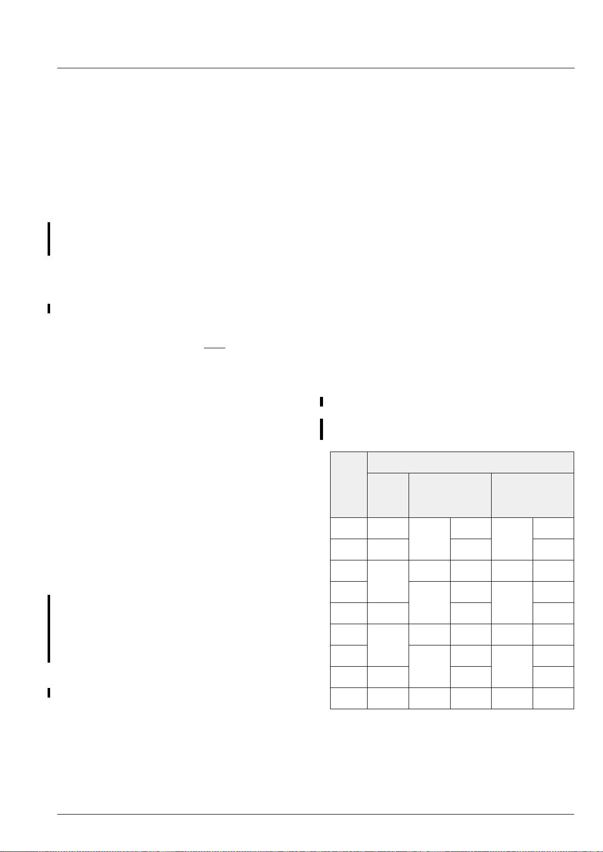
part. Th e volume range is −114...+12 dB wit h an addi-
Fig. 2–2: Signal flow block diagram of Audio Codec
2.4.2.3. Automatic Volume Control (AVC)
In a collection of tracks from different sources fairly
often the average volume level varies. Especially in a
noisy listening environment the user must adjust the
volume to achieve a comfortable listening en joyment.
The Automatic Volume Correction (AVC) solves this
problem by equalizing the volume level.
To prevent clipping, the AVC’s gain decreases quickly
in dynamic boost conditions. To suppress oscillation
effects, the gain increases rather slowly for low level
inputs. The decay time is programmable by means of
the AVC register (see Table 3–13 on page 42).
For input levels of -18 dBr to 0 dBr, the AVC maintains
a fixed output level of -9 dBr. Fig. 2–3 shows the AVC
output level versus its input level. For volume and
baseband registe rs set to 0 dB, a level of 0 dBr corresponds to full scale input/output.
tional mute position. A balance function is provided.
2.4.3. D/A Converters
A pair of Micronas’ unique multibit sigma-delta D/A
converters is used to convert th e audio data with high
linearity and a superior S/N. In order to attenuate highfrequency noise caused by noise-shaping, internal
low-pass filters are included. They require additional
external capacitors between pins FILTx and OUTx.
2.4.4. Output Amplifiers
The integrated output amplifiers are capable of directly
driving stereo headphones or loudspeakers of
16...32Ω impedance via 22-Ω series re s i sto rs. I f m o re
output power is required, the right output signal can be
inverted and a single loudspeaker can be connected
as a bridge between pins OUTL and OUTR. In this
case for optimized power the source should be set to
mono.
MASF
DAC
DAC
OUTL
OUTR
R≥32
Fig. 2–4: Bridge operation mode
10 Micronas
Ω
Page 11
ADVANCE INFORMATION MAS 35x9F
2.5. Clock Management
The MAS 35x9F is driven by a single crystal-controlled
clock with a frequency of 18.432 MHz. It is possible to
drive the MAS 35x9F with other reference clocks. In
this case, the nominal crystal frequen cy must be written into memory location D0:348. The crystal clock
acts as a reference for the embedded syn thesizer that
generates the internal clock.
For compressed audio data re cepti on, the MA S 35x9F
may act either as the clock master (De mand Mode) or
as a slave (Broadcast Mode) as defined by bit 1 in
IOControlMain memory cell (see Table 3–7 on
page 32). In both mode s, the output of the clock synthesizer depends on t he sample rate of the decoded
data stream as shown in Table 2–1.
In the BROADCAST MODE (PLL on), the incoming
audio data controls the clock synthesizer via a PLL.
In the DEMAND MODE (PLL off) t he MAS 35x9F acts
as the system master clock. The da ta transfer is triggered by a demand signal at pin EOD
.
2.5.1. DSP Clock
The DSP clock has sep arate divider. For power conservation it is set to th e lowest acceptable rate of the
synthesizer clock which is capable to allow the processor core to perform all tasks.
2.6. Power Supply Concept
The MAS 35x9 F ha s been de si gn ed for minimal power
dissipation. In order to optimize the battery management in por table players, two DC/DC converters have
been implemented to supply the complete portable
audio player with regulated voltages.
2.6.1. Power Supply Regions
The MAS 35x9F has five power supply regions.
The VDD/VSS pin pa ir suppl ies all di gital p ar ts inc lud-
ing the DSP core, the XVDD/XVSS pin pair is connected to the digital signal pin output buffers, the
AVDD0/AVSS0 supply is for the analog output amplif iers, AVDD1/AVSS1 for all other analog circuits like
clock oscillator, PLL circuits, system clock synthesi zer
and A/D and D/A converter s. The I
own supply region via pin I 2CVDD. Connecting this to
the microcontroller supply assures that the I
2
C interface has an
2
C bus
always works as long as t he mic rocontr olle r is al ive so
that the operating modes can be selected.
Beside these regions, the DC/DC converters have
start-up circuits of their own which get their power via
pin VSENSx .
Table 2–1: Settings of bits 8 and 17 in OutClkConfig
and resulting CLKO output frequencies
Output Frequency at CLKO/MHz
2.5.2. Clock Output At CLKO
If the DSP or audio codec functions are enabled (bits
11 or 10 in the Control Register at I
), the reference clock at pin CLKO is derived from
6a
hex
2
C subaddress
the synthesizer clock.
Dependent on the sample rate of the decoded signal a
scaler is applied which auto m at ic ally div id es the c lo ckout by 1, 2, or 4, as shown in Table 2–1. An additional
division by 2 may be selected by setting bit 17 of the
OutClkConfig memory cell (see Table 3–7 on
page 32). The scaler can be disabled by setting bit 8 of
this cell.
The controlling at OutClkConfig is only possible as
long as the DSP is ope rational (bit 10 of the Control
Register). Setting s remain valid if the DSP i s disabled
by clearing bit 10.
Synth.
fs/kHz
Clock
bit 8=1
48 24.576
44.1 22.5792 22.5792 11.2896
32
Scaler On
bit 8=0, bit 17=0
Extra Division
bit 8=0, bit 17=1
24.576
512⋅f
s
24.576 384⋅fs 12.288
768⋅f
s
256⋅fs
Scaler Plus
12.288
24.576
24
512⋅f
22.05 22.5792 11.2896 5.6448
16
768⋅f
12.288
s
12.288 384⋅fs 6.144
s
256⋅fs
6.144
24.576
12
512⋅f
11.025 22.5792 5.6448 2.8224
8 24.576 768⋅f
6.144
s
6.144 384⋅fs 3.072
s
256⋅fs
3.072
Micronas 11
Page 12

MAS 35x9F ADVANCE INFORMATION
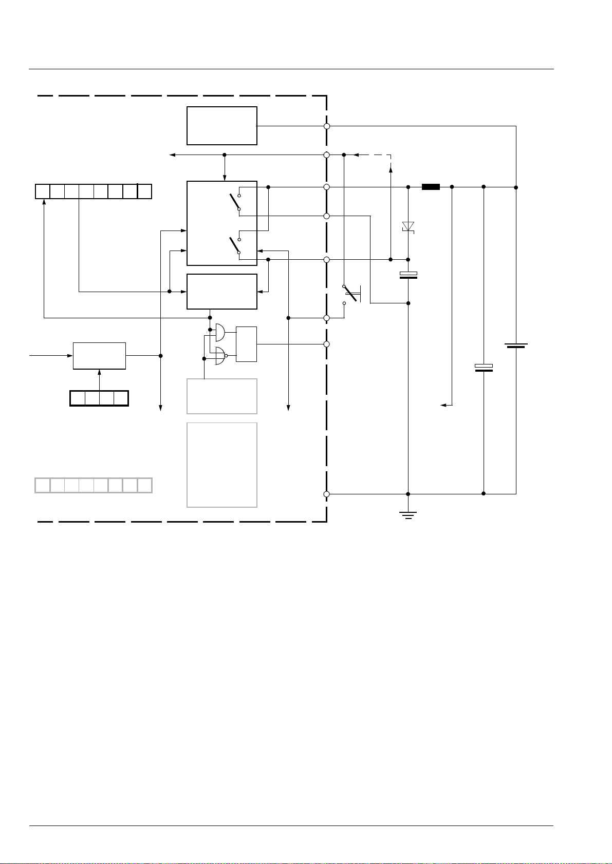
2.6.2. DC/DC Converters
The MAS 35x9F has two em bed ded high-performance
step-up DC/DC co nverters with sy nchronous recti fiers
to supply both the DSP core itself and external circuitry
such as a controller or flas h memory at two different
voltage levels. An overview is given in Fig. 2–9 on
page 14.
The DC/DC converters are designed to generate an
output voltage between 2.0 V and 3.5 V which ca n be
programmed separately for each converter via the I
2
interface (see table 3.3). Bot h converters are of bo otstrapped type allowing to start up from a voltage down
to 0.9 V f or us e wi th a si ngl e ba tt ery or Ni Cd/N iMH c el l.
The default output voltages a re 3.0 V. Both converters
are enabled with a high level at pin DCEN and
enabled/disabled by the I
2
C interface.
The MAS 35x9F DC/DC converters feature a constantfrequency, low noise pulse width modulation (PWM)
mode and a low quiescent current, pulse frequency
modulation (PFM) mode for improved efficiencies at
low current loads. Both m odes – PWM or PFM – ca n
be selected indepe ndently for each converter via I
2
interface. The default mode is PWM.
In PWM mode the switching frequen cy of the power-
MOSFET-switches is derived from the crystal oscillator. Switching harmonics generated by constant frequency operation are consistent and predictable.
When the audio codec is enabled the switching frequency of the conver ters is synchroni sed to the audi o
codec clock to avoid interferences into the aud io band .
The actual switching frequency can be selected via the
2
C-interface between 300 kHz and 580 kHz (for
I
details see DCFR Register in Table 3–3 on page 21).
In PFM operation mode the switching frequency is
controlled by the converters themself, it will be just
high enough to service the output load thus resulting in
the best possible effic iency at low current lo ads. PFM
mode does not need a clock signal from the crystal
oscillator. If both converters do not use the PWMmode, the cryst al clock will be shut down as lon g it is
not needed from other internal blocks.
The synchronous rectifier bypasses the external
Schottky diode to re duce losses caused by the d iode
forward voltage providing up to 5% efficiency imp rovement. By default, the P-channel syn chronous rectifier
switch is turned on when the voltage at pin(s) DCS On
exceeds the converter’s output voltage at pin(s)
VSENSn and turns off when the inductor current drops
below a threshold. If one or both converters are disabled, the corresponding P-channel switch will be
turned on, connecting the battery voltage to the DC/
DC converters output voltage at pin VSENSn. However, it is possible to individuall y disable both sy nchronous rectifier switches by setting the corresponding
bits (bit 8 and 0 in DCCF-register).
If both DC/DC-converters are off, a high signal may be
applied at pin DCE N. This will star t the converters in
their default mode (PWM with 3.0 V output voltage).
The PUP signal will change from low to high when both
converters have reached their nominal output voltage
and will return to low when both converters output voltages have dropped 200 mV below their programmed
output voltage. The signal at pin PUP ca n be used to
control the reset of an external microcontroller (see
Section 2.10.2. on page 16 for details on start up procedure).
C
If only DC/DC-converter 1 is used, the output of the
unused converter 2 (VSEN S2) must be connected to
the output of converter 1 (VSENS1) to make the PUP
signal work proper ly. Also, if a DC/DC-converter is not
used (no inducto r connected), the pin DCSO must be
left vacant.
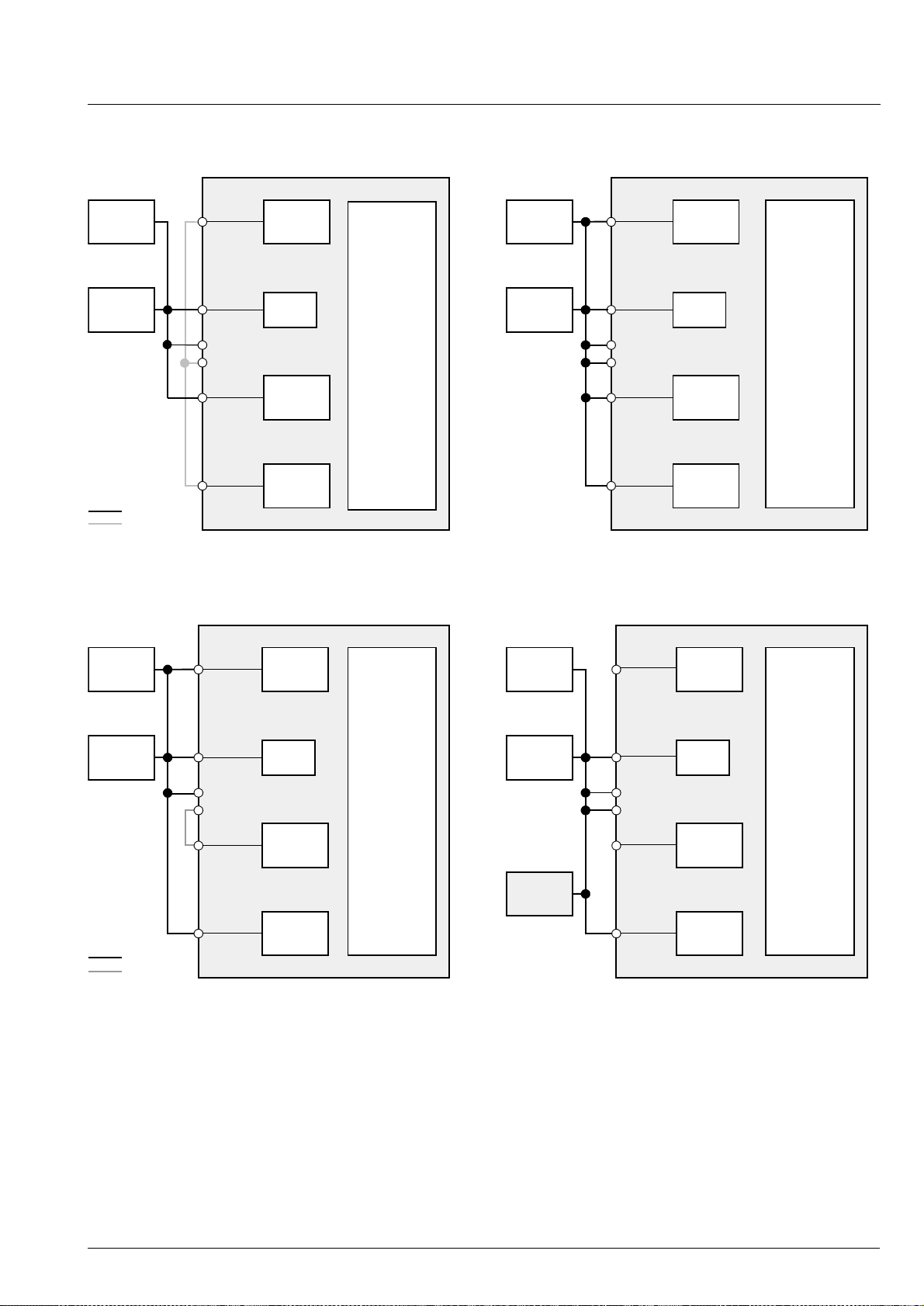
2.6.3. Power Supply Configurations
One of the following supply configurations may be
used:
C
– Power-optimized solution (recommended opera-
tion). DC/DC 1 (e.g. 2.2 V) drives the MAS 35x9F
DSP and the audio circuitry, DC/DC 2 (e.g. 2.7 V)
supplies controller and flash (see Fig. 2–5 on
page 13)
– Volume-optimized solution. DC/DC 1 (e.g. 2.7 V)
supplies controller, flash and MAS 35x9F audio
parts, DC/DC 2 generates e.g. 2.2 V for the
MAS 35x9F DSP (see Fig. 2–6 on page 13).
– Minimized external components. DC/DC 1 operates
on e.g. 2.7 V and feeds all components, DC/DC 2
remains off (see Fig. 2–7 on page 13).
– External power supply . All components are powered
by an external source, no DC/DC converter is used
(see Fig. 2–8 on page 13).
If DC/DC converter 1 is used, it must supply the analog
circuits (pins AVDD0, AVDD1) of the MAS 35x9F.
If only one DC/DC converter is required, DC/DC1 must
be used. Pin DCSO2 must be left vacant, pin VS ENS 2
should be connected to pin VSENS1.
If the DC/DC converters a re not us ed, pi n DCEN mus t
be connected to VSS, DCSOx must be left vacant.
12 Micronas
Page 13
ADVANCE INFORMATION MAS 35x9F
Flash
C
µ
VSENS1
2
CVDD
I
XVDD
VDD
VSENS2
AVDD0/1
DC/DC 1
on
2
I
C
DC/DC 2
on
Analog
Parts
e.g. 2.7 V
e.g. 2.2 V
Fig. 2–5: Solution 1: Power-optimized
Flash
VSENS1
DC/DC1
on
DSP
Flash
e.g. 2.7 V
C
µ
VSENS1
2
CVDD
I
XVDD
VDD
VSENS2
AVDD0/1
DC/DC1
on
I2C
DC/DC2
off
Analog
DSP
Parts
Fig. 2–7: Solution 3: Minimized components
Flash
VSENS1
DC/DC1
off
2
CVDD
C
µ
e.g. 2.7 V
e.g. 2.2 V
I
XVDD
VDD
VSENS2
AVDD0/1
I2C
DC/DC2
on
Analog
Parts
Fig. 2–6: Solution 2: Volume-optimized
DSP
2
I
C
µ
CVDD
VDD
XVDD
VSENS2
I2C
DC/DC2
off
External
Supply
AVDD0/1
e.g. 2.7 V
Analog
Parts
Fig. 2–8: Solution 4: External power supply
DSP
Micronas 13
Page 14
MAS 35x9F ADVANCE INFORMATION
to I2C interface
DCCF (76
15 8
)
hex
set voltage
frequency
system
or crystal
clock
divider
factor
30
DCFR (77
hex
)
battery
voltage
monitor
DC/DC
converter 2
voltage
monitor
voltage
monitor
VBAT
PUP
supply
StartPUP2
output 1
D1
+
−
330µF
L1
22µH
C1
V
in
+
−
+
−
I2CVDD
DCSO2
DCSG2
VSENS2
DCEN
S
R
DCCF (76
70
hex
)
converter 1
VSS
Fig. 2–9: DC/DC converter overview. The DCEN input must be connected to pin I2CVDD via the start-up push
button.
2.7. Battery Voltage Supervision
A battery voltage super vision circuit (at pin VBAT) is
provided which is independe nt of the DC/DC converters. It can be programmed to supervise one or two battery cells. The voltage is measured by subsequently
setting a series of voltage t hr eshol ds and c he cking the
DC/DC
respective comparison result in register 77
hex
.
14 Micronas
Page 15

ADVANCE INFORMATION MAS 35x9F
2.8. Interfaces
2
The MAS 35x9F uses an I
input interface for MPEG bit streams, and a digital
audio output inter face for the decoded audio data (I
C control interface, a serial
2
or similar). Alter natively, SPDIF input and output interfaces can be used. A parallel I/O interface (PIO) m ay
be used for fast data exchange.
2
2.8.1. I
For controlling and program download purposes, a
standard I
C Control Interface
2
C slave interface is implemented. A detailed
description of all functions can be found in Section 3.
2.8.2. SPDIF Input Interface
The SPDIF interface receives a one-wire serial bus
signal. In addition to the signal input pin SPDI1/SPDI2,
a reference pin SPDIR is provided to support balanced
signal sources or twisted pair transmission lines.
The synchronization time on the input signal is
<50ms.
In case of the Deman d Mode (see Section 2.5.), the
signal clock coming from the data source must be
higher than the nominal data transmission rate (e.g.
128 kbit/s). Pin EOD
S
whenever the input buffer of the MAS 35x9F is filled.
is used to interrupt the data flow
For controlling details please refer to Table 3–7 on
page 32.
2.8.5. Multiline Serial Output (SDO)
The serial au dio output interface of the MAS 35x9F is
a standard I
2
S-like interface consisting of the data
lines SOD, the word strobe SOI and t he clock signal
SOC. It is possible to choose between two standard
interface configurations (16-bit data words with word
strobe time offset or 32-bit data words with inverted
SOI-signal).
If the serial output generates 32 bits per audio sample,
only the first 20 bits will carry valid audio data. The
12 trailing bits are set to zero by default.
2.8.6. Parallel Input/Output Interface (PIO)
The SPDIF input signal can also be switched to the
SPDO pin. In this case the analog input ci rcuit of the
SPDIF inputs (see Fig. 4–18 on page 59) restores the
SPDIF input signal to a full swing signal at SPDO.
For controlling details please refer to Table 3–7 on
page 32.
2.8.3. S/PDIF Output
In the next version of the IC the S/PDIF ou tput of the
baseband audio signals will be provided at pin SPDO.
2.8.4. Multiline Serial Audio Input (SDI, SDIB)
There are two multiline serial audio input interfaces
(SDI, SDIB) each consisting of the three pins SI(B)C,
SI(B)I, and SI(B)D. The standard firmware only supports SDIB for bitstream signals.
The interfaces can be configured as continuous bit
stream or word-oriented inputs. For the MPEG bitstreams the word strobe pin SI BI must always be connected to V
, bits must be sent MS B first as creat ed
SS
by the encoder.
The parallel interface of the MAS 35x9F consists of the
8 data lines PI12...PI19 (MSB) and the control lines
, PR, PRTR, PRTW, and EOD. It can be used for
PCS
data exchange with an external memory, for fast program download and for other special purposes as
defined by the DSP software.
For MPEG-data input, the PI O inte rface is ac tivated by
setting bits 9,8 in D0:346 to 01. For the handshake
protocol please refer to Section 4.6.3.6. on page 72
If the optional downloadable software uses th e inputs
for PCM data, the interface acts as a I
2
S-type with
SI(B)I as a word strobe.
Micronas 15
Page 16
MAS 35x9F ADVANCE INFORMATION
V
h
V
l
t
read
t
frame
= 24...72 ms
2.9. MPEG Synchronization Output
The signal at pin S YNC is set to ‘1’ after the inter nal
decoding for the MPEG header has been finished for
one frame. The rising e dge of this signal can be used
as an interrupt input for the controller that triggers th e
read out of the control in formation and ancillar y data.
As soon as the MAS 35x9F has received the SYNC
reset command (see Section 3.3.1.12. on page 28),
the SYNC signal is clea red. If the controller does not
issue a reset comman d, the SY NC signal returns to ’0’
as soon as the decodi ng of the next MPEG frame is
started. MPEG status and ancillary data become
invalid until the frame is completely de coded and the
signal at pin SYNC rises again. The controller must
have finished reading all MPEG information before it
becomes invalid. The MPEG Layer 2/3 frame lengths
are given in Table 2–2. AAC has no fixed frame length.
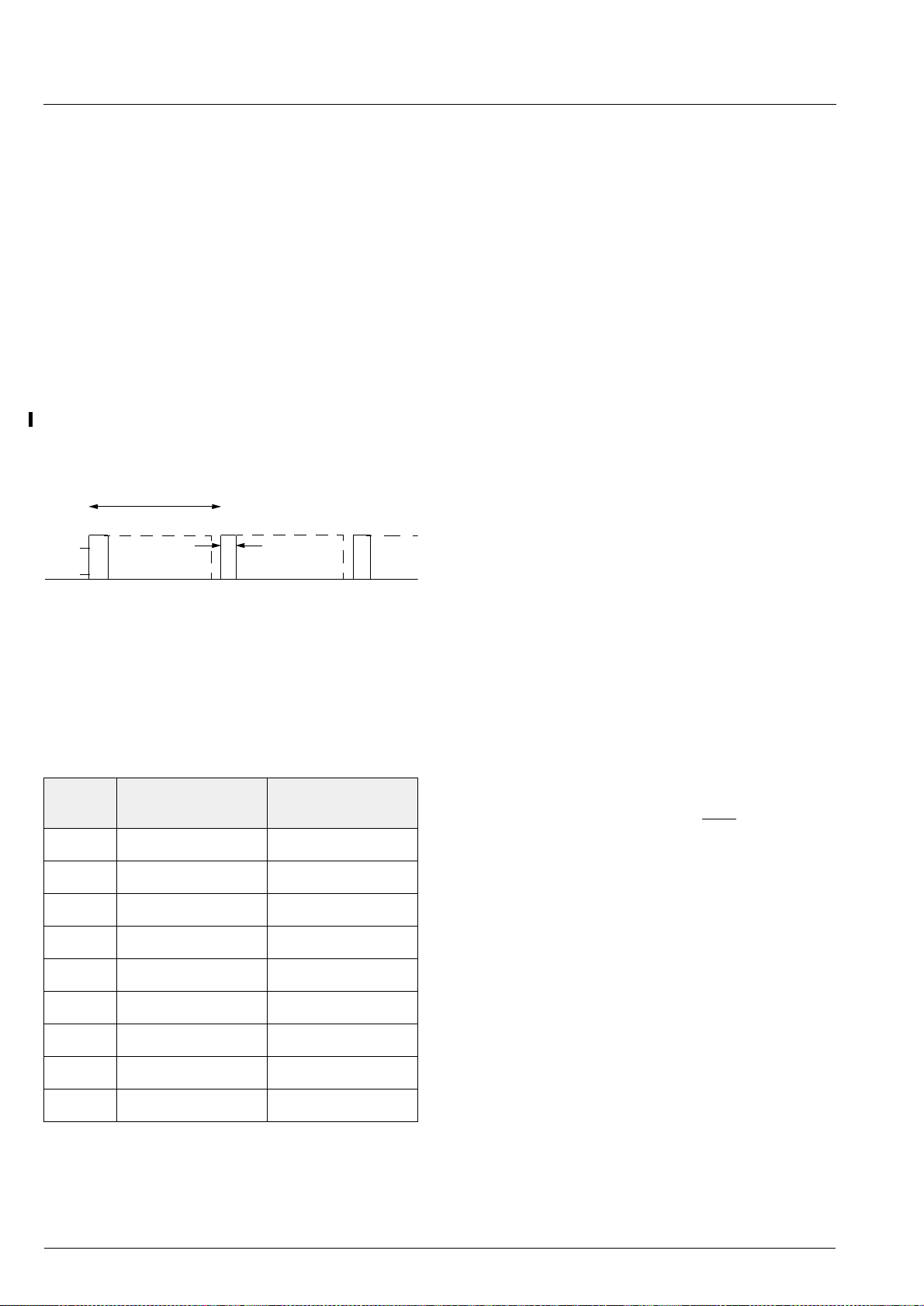
Fig. 2–10: Schematic timing of the signal at pin SYNC.
The signal is cleared at t
when the controller has
read
issued a Clear SYNC Signal command (see Section
3.3.1.12. on page 28). If no command is issued, the
signal returns to ’0’ just before the decoding of the next
MPEG frame.
Table 2–2: Frame length in MPEG Layer 2/3
fs/kHz Frame Length
Layer 2
Frame Length
Layer 3
48 24 ms 24 ms
44.1 26.12 ms 26.12 ms
32 36 ms 36 ms
24 24 ms 24 ms
22.05 26.12 ms 26.12 ms
16 36 ms 36 ms
12 not available 48 ms
11.025 not available 52.24 ms
8 not available 72 ms
2.10.De fau lt Operatio n
This sections refers to the standard operation mode
”power-optimized solution” (see Section 2.6.3.).
2.10.1.Stand-by Functions
After applying the battery voltage, the system will
remain stand-by, as long as the DCEN pin level is kept
low. Due to the low stand-by current of CMOS circuit s,
the battery may remain connected to DCSOn/VSENSn
at all times.
2.10.2.Power-Up of the DC/DC Converters and Reset
The battery voltage must b e appl ied to p in DCSOn via
the 22-µH inductor and, further more, to the sense pin
VSENSn via a Schottky diode (see Fig. 2–9 on
page 14).
For start-up, the pin DCEN must be co nnected via an
external “start” push button to the I2CVDD supply,
which is equivalent to the battery supply voltage
(> 0.9 V) at start-up.
The supply at DCEN must be appli ed until the D C/DC
converters have started up (signal at pin PUP) and
then removed for normal operation.
As soon as the outp ut voltag e at VS E NSn r eaches th e
default voltage monitor reset level of 3.0 V, the respective internal PUPn bit will be set. When both PUPn bits
are set, the signa l at pin PUP will go high and can be
used to start and reset the microcontroller.
2
Before transmitting any I
must issue a power-on reset to pin POR
supply pin I2CVDD assures that the I
C commands, the controller
. The separate
2
C interface
works indepentently of the DSP or the audio codec.
Now the desired supply voltage can be programmed at
2
C subaddress 76
I
The signal at pin PUP will return to low only when both
PUPn flags (I
2
.
hex
C subaddress 76
) have returned to
hex
zero. Care must be taken when changing bo th DC/DC
output voltages to higher values. In this case, both output voltages are momentarily insufficient to keep the
PUPn flags up; the resulting dip in the signal at the
PUP pin may in turn reset the microcontroller. To avoid
this condition, on ly one DC/DC output voltage should
be changed at a time. Before modifying the second
voltage, the microcontroller must wait for the PUPn flag
of the first voltage to be set again.
The operating mode (pulse width modulation or pulse
frequency modula tion, sy nchron ized rect ifier for higher
efficiency) are control led at I
16 Micronas
operating frequency at I
2
C subaddress 76
2
C subaddress 77
hex
.
hex
, the
Page 17

ADVANCE INFORMATION MAS 35x9F
2.10.3.Control of the Signal Processing
Before starting the DSP, the controller should check for
a sufficient voltage supply (respective flag PUPn at I
subaddress 76
appropriate b it in the Co ntrol register (I
). The nominal freque ncy of the crys tal oscillator
6a
hex
). The DSP is enabled by setting the
hex
2
C subaddress
2
must be written into D0:348. After an initialization
phase of 5 ms, the DSP data registers can be
accessed via I
2
C.
Input and output control is performed via memory location D0:346 and D0:347. The serial input interface
SDIB is the default. The d ecoded a udio can be routed
to either the SPDIF, the SDO and the analog ou tputs.
The output clock signal at pin CLKO is defined in
D0:349.
All changes in the D0-mem ory cells become effective
synchronously upon setting the LSB o f Main I/O Con-
trol (see Table 3–7 on page 32). Therefore, this cell
should always be written at last.
The digital volume contr ol (see Table 3–7 on page 32)
is applied to the output signal of the DSP. The decoded
audio data will be available at the SPDO output interface in the next version.
2.10.5.Power-Down
All analog outputs s hould be muted and the A/D and
C
the D/A converters must be switched off (register
00 10
and 00 00
hex
at I2C subaddress 6c
hex
hex
). The
DSP and the audio codec must be disabled (clear
DSP_EN and CODEC_EN bits in the Control register,
2
C subaddress 6a
I
enable flags in the Control register (I
), the microcont roller can power down the c om-
6a
hex
). By clearing both DC/DC
hex
2
C subaddress
plete system.
The DSP does not have to be star ted if its functions
are not needed, e.g. for routing audio via the A/D and
the D/A converters through the codec part of the IC.
2.10.4.Start-up of the Audio Codec
Before enabling the audio codec, the controlle r should
check for a sufficient voltage supply (respective flag
PUPn at I
The audio codec is enabled by setting the app ropriate
bit at the Control register (I
an initialization phase of 5 ms, the DSP data registe rs
can be accessed via I
ers must be switched on explicitly (00 00
address 6c
data from the A/D converte rs or th e output o f the DSP,
or a mix of bo th
subaddress 6c
ume (00 10
2
C subaddress 76
2
C.The A/D and the D/A convert-
). The D/A converters may either ac cept
hex
1)
(register 00 06
). Finally, an appropriate output vol-
hex
at I2C subaddress 6c
hex
).
hex
2
C subaddress 6a
hex
and 00 07
hex
hex
at I2C sub-
) must be
hex
hex
). After
at I2C
selected.
1)
mixer available in version A2 and later; in version A1
please use selector 00 0f
hex
.
Micronas 17
Page 18
MAS 35x9F ADVANCE INFORMATION
3. I2C Interface
3.1. General
3.1.1. Device Address
2
Controlling the MAS 35x9F is done via an I
interface. The device addresses are 3C/3E
write) and 3D/3F
1. The device address pair 3C/3D
(device read) as shown in Table 3–
hex
applies if the DVS
hex
C slave
(device
hex
pin is connected to VSS, the device address pair 3E/
applies if the DVS pin is connected to VDD.
3F
hex
Table 3–1: I
2
C device address
A7 A6 A5 A4 A3 A2 A1 W/R
001111DVS0/1
2
C clock synchronization is used to slow down the
I
interface if required.
2
3.1.2. I
C Registers and Subaddresses
The interface uses one level of subaddresses. The
MAS 35x9F interface has 7 subaddresses allocated for
the correspondin g I
2
C registers. The registers can be
divided into three categories as shown in Table 3–2.
The address 6A
is used for basic con trol, i.e. reset
hex
and task select. The other addresses are used for data
transfer from/to the MAS 35x9F.
Table 3–2: I2C subaddresses
Subaddress
(hex)
I2CRegister
Name
Function
Direct Configuration
6A CON-
TROL
Controller writes to
MAS 35x9F control register
76 DCCF Controller writes to first
DC/DC configuration register
77 DCFR Controller writes to
second DC/DC config reg.
DSP Core Access
68 DATA
(WRITE)
69 DATA
(READ)
Controller writes to
MAS 35x9F DSP
Controller reads from
MAS 35x9F DSP
Codec Access
6C CODEC
(WRITE)
6D CODEC
(READ)
Controller writes to
MAS 35x9F codec register
Controller reads from
MAS 35x9F codec register
2
C registers of the MAS 3 5x9F are 16 bits wide,
The I
the MSB is denoted as bit[15] . Transmissions via I
2
bus have to take place in 16-bit words (two byte transfers, MSB sent first); thus, for each register access,
two 8-bit data words must be sent/received via I
2
bus.
C
C
18 Micronas
Page 19
ADVANCE INFORMATION MAS 35x9F
3.1.3. Naming Convention
The description of the various controller commands
uses the following formalism:
– Abbreviations used in the following descriptions:
a address
d data value
n count value
o offset value
r register number
x don’t care
– A data value is split into 4-bit nibbles which are num-
bered beginning with 0 for the least significant nibble.
– Data values in nibbles are always shown in hexa-
decimal notation.
– A hexadecimal 20-bit number d is written, e.g. as
d = 17C63
d0 = 3
hex
d4 = 1
hex
– Variables used in the following descriptions:
2
C address:
I
DW 3C/3E
DR 3D/3F
, its five nibbles are
hex
, d1 = 6
, d2 = C
hex
.
hex
hex
, d3 = 7
hex
hex
, and
DSP core:
data_write 68
data_read 69
hex
hex
Codec:
codec_write 6C
codec_read 6D
hex
hex
– Bus signals
SStart
PStop
A ACK = Acknowledge
N NAK = Not acknowledge
– Symbols in the telegram examples
< Start Condition
> Stop
dd
xx
data bytes
ignore
All telegram numbe rs are hexadecimal, data originating from the MAS 35x9F are greyed.
Example:
dd dd
<DW 68
<DW 69 <DR
> write data to DSP
dd dd
> read data from DSP
and stop with NAK
2
Fig. 3–1 shows I
C bus protocols for write and read
operations of the interface; the read operatio ns requir e
an extra start condition and repetition of the chip
address with the device read command (DR). Fields
with signals/data or iginating from the MAS 35x9F are
marked by a gray background. Note that in some
cases the data reading proc ess must be conc luded by
a NAK condition.
Example: I
2
C write access
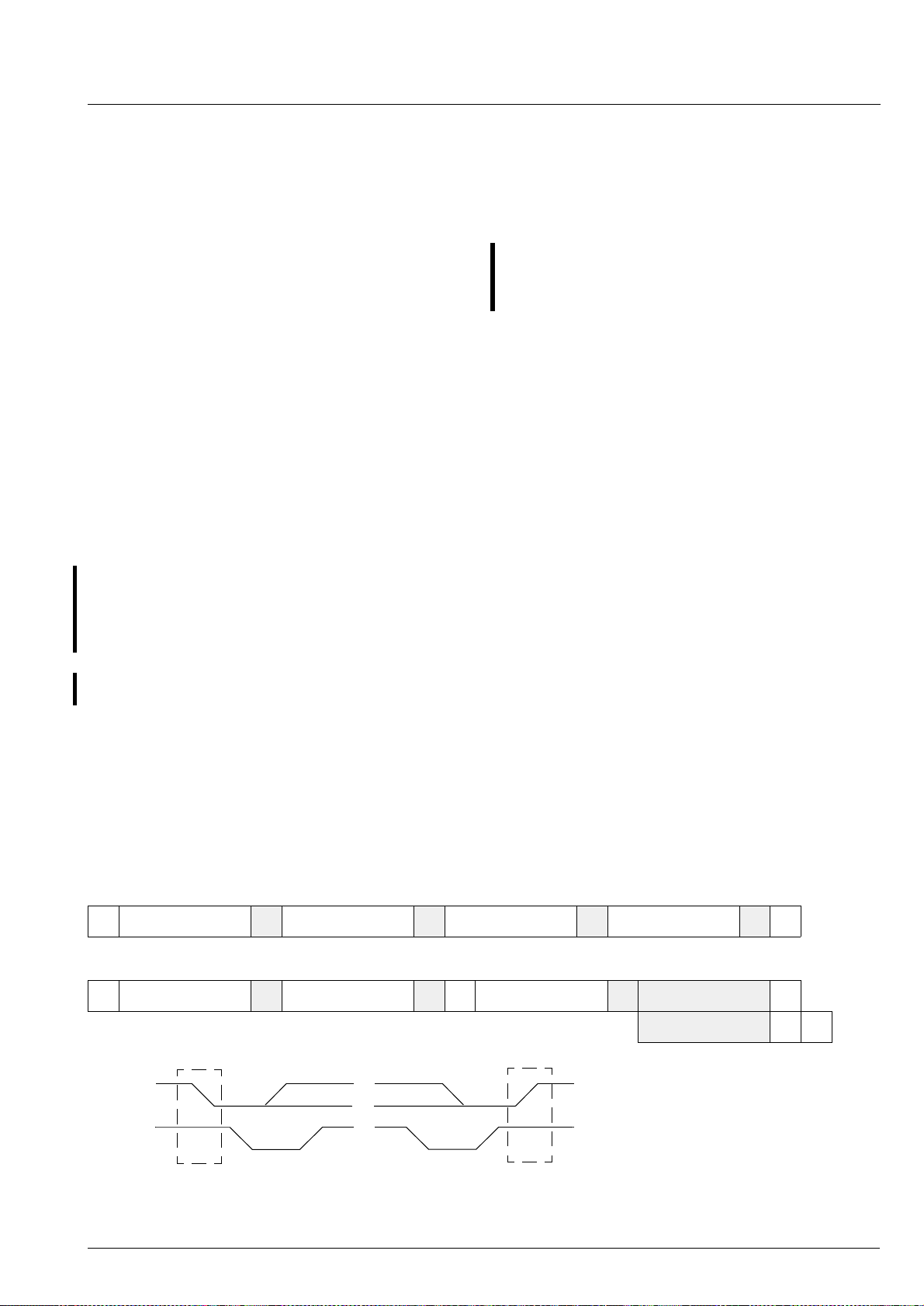
low data wordAhigh data wordAsubaddressADWS A P
2
Example: I
C read access
high data wordADRSAsubaddressADWS A
NPlow data word
SDA
SCL
S
Fig. 3–1: Example of an I
2
C bus protocol for the MAS 35x9F (MSB first; data must be stable while clock is high)
1
0
P
A
=
0 (ACK)
=
N
S
P
1 (NAK)
=
Start
=
Stop
Micronas 19
Page 20

MAS 35x9F ADVANCE INFORMATION
AP
d1,d0
AAAS
DW subaddress d3,d2
3.2. Direct Configuration Registers
The task selection of the DSP and the DC/DC converters are controlled i n the direct configuration registe rs
Control, DCCF, and DCFR.
3.2.1. Write Direct Configuration Registers
The write protoc ol for the direct confi guration re gisters
only consists o f device address, subaddress and one
16-bit data word.
3.2.2. Read Direct Configuration Register
1) send subaddress
DW subaddress
SAAP
2) get register value
DW subaddress DR
SAASA
d3,d2 d1,d0
AN
P
To check the PUP1 and PUP2 power-up flags, it is
necessary to read back the content of the direct configuration registers.
20 Micronas
Page 21

ADVANCE INFORMATION MAS 35x9F
Table 3–3: Direct Configuration Registers
I2C Sub-
Function Name
address
(hex)
6A Control Register (reset value = 30 00
bit[15:14] Analog Supply Voltage Range
Code AGNDC recommended for voltage range of AVDD
00 1.1 V 2.0 ... 2.4 V (reset)
01 1.3 V 2.4 ... 3.0 V
10 1.6 V 3.0 ... 3.6 V
11 reserved reserved
Higher voltage ranges permit higher output levels and thus a better signal-to-
noise ratio.
bit[13] enable DC/DC 2 (reset=1)
bit[12] enable DC/DC 1 (reset=1)
Both DC/DC converters are switched on by default.
bit[11] enable and reset audio codec
bit[10] enable and reset DSP core
For normal operation (MPEG-decoding and D/A conversion), both, the DSP
core and the audio codec have to be enabled after the power-up procedure.
The DSP can be left off if an audio signal is routed from the analog inputs to
the analog outputs (set bit[15] in codec register 00 0F
can be left off if the DSP uses digital inputs and outputs only.
hex
)
). The audio codec
hex
CONTROL
6B
bit[9] reset codec
bit[8] reset DSP core
bit[7] disable task 7 of DSP core
bit[6] disable task 6 of DSP core
bit[5] disable task 5 of DSP core
bit[4] disable task 4 of DSP core
bit[3] set task 3 of DSP core
bit[2] set task 2 of DSP core
bit[1] set task 1 of DSP core
bit[0] set task 0 of DSP core
1)
bit[7]
bit[6:0]
1)
bit[15:8] reserved, must be set to zero
1)
enable XTAL input clock di vider
(extended crystal range up to 28 MHz)
reserved, must be set to zero
DSP_TASK
bit[7] disable task 7 of DSP core
bit[6] disable task 6 of DSP core
bit[5] disable task 5 of DSP core
bit[4] disable task 4 of DSP core
bit[3] set task 3 of DSP core
bit[2] set task 2 of DSP core
bit[1] set task 1 of DSP core
bit[0] set task 0 of DSP core
Unless downloaded optional software is used, the bits 7...0 must be set to
zero.
1)
available in the next version
Micronas 21
Page 22

MAS 35x9F ADVANCE INFORMATION
Table 3–3: Direct Configuration Registers
I2C Sub-
Function Name
address
(hex)
76 DCCF Register (reset = 5050
DC/DC Converter 2
bit[15] PUP2: Voltage monitor 2 flag (readback)
bit[14:11] Voltage between VSENS2 and DCSG2
Code Nominal set level reset level
output volt. of PUP2 of PUP2
1111 3.5 V 3.4 V 3.3 V
1110 3.4 V 3.3 V 3.2 V
1101 3.3 V 3.2 V 3.1 V
1100 3.2 V 3.1 V 3.0 V
1011 3.1 V 3.0 V 2.9 V
1010 3.0 V 2.9 V 2.8 V (reset)
1001 2.9 V 2.8 V 2.7 V
1000 2.8 V 2.7 V 2.6 V
0111 2.7 V 2.6 V 2.5 V
0110 2.6 V 2.5 V 2.4 V
0101 2.5 V 2.4 V 2.3 V
0100 2.4 V 2.3 V 2.2 V
0011 2.3 V 2.2 V 2.1 V
0010 2.2 V 2.1 V 2.0 V
0001
0000
1)
1)
2.1 V 2.0 V 1.9 V
2.0 V 1.9 V 1.8 V
) DCCF
hex
bit[10] Mode
1 Pulse frequency modulation (PFM)
0 Pulse width modulation (PWM) (reset)
bit[9] reserved, must be set to zero
bit[8] Disable synchronized rectifier
1 disable synchronized recitifier
0 enable synchronized recitifier (reset)
The DC/DC converters are up-converters only. Thus, if the battery voltage is
higher than the selected nominal voltage, the output voltage will exceed the
nominal voltage.
1)
refer to Section 4.6.2. on page 61
22 Micronas
Page 23

ADVANCE INFORMATION MAS 35x9F
Table 3–3: Direct Configuration Registers
I2C Subaddress
(hex)
76
(continued)
Function Name
DC/DC Converter 1
bit[7] PUP1: Voltage monitor 1 flag (readback)
bit[6:3] Voltage between VSENS1 and DCSG1 (see table above)
bit[2] Mode
1 Pulse frequency modulation (PFM)
0 Pulse width modulation (PWM) (reset)
bit[1] reserved, must be set to zero
bit[0] Disable synchronized rectifier
1 disable synchronized recitifier
0 enable synchronized recitifier (reset)
Note, that the reference voltage for DC/DC converter 1 is derived from the
main reference source supplied via pin AVDD1. Therefore, if this DC/DC converter is used, its output must be connected to the analog supply.
The DC/DC converters are up-converters only. Thus, if the battery voltage is
higher than the selected nominal voltage, the output voltage will exceed the
nominal voltage.
Micronas 23
Page 24

MAS 35x9F ADVANCE INFORMATION
Table 3–3: Direct Configuration Registers
I2C Subaddress
(hex)
77 DCFR Register (reset = 00
Function Name
Battery Voltage Monitor
bit[15] Comparison result (readback)
1 input voltage at pin VBAT above defined threshold
0 input voltage at pin VBAT below defined threshold
bit[14] Number of battery cells
0 1 cell (range 0.8...1.5 V) (reset)
1 2 cells (range 1.6...3.0 V)
bit[13:10] Voltage threshold level
1 cell 2 cells
1111 1.5 3.0 V
1110 1.45 2.9 V
...
0010 0.85 1.7 V
0001 0.8 1.6 V
0000 Battery voltage supervision off (reset)
bit[9:8] Reserved, must be set to 0
The result is stable after 1 ms after enabling. The setup time for switching
between two thresholds is negligibly small.
) DCFR
hex
For power management reasons, the battery voltage monitor should be
switched off by setting bit[13:10] to zero when the measurement is completed.
DC/DC Converter Frequency Control (PWM)
bit[7:4] Reserved, must be set to 0
bit[3:0] Frequency of DC/DC converter
Reference: 24.576 22.5792 18.432 MHz
0111 315.1 289.5 297.3 kHz
0110 323.4 297.1 307.2 kHz
0101 332.1 305.1 317.8 kHz
0100 341.3 313.6 329.1 kHz
0011 351.1 322.6 341.3 kHz
0010 361.4 332.0 354.5 kHz
0001 372.4 342.1 368.6 kHz
0000 384.0 352.8 384.0 kHz (reset)
1111 396.4 364.2 400.7 kHz
1110 409.6 376.3 418.9 kHz
1101 423.7 389.3 438.9 kHz
1100 438.9 403.2 460.8 kHz
1011 455.1 418.1 485.1 kHz
1010 472.6 434.2 512.0 kHz
1001 491.5 451.6 542.1 kHz
1000 512.0 470.4 576.0 kHz
2
If the audio codec is not enabled (bit 11 of the Control register at I
dress 6A
from the crystal frequency (nominal 18.432 MHz). Otherwise, the synthesizer
clock is used as the reference (please refer to the respective column in
Table 2–1 on page 11).
is zero), the clock for the DC/DC converters is directly derived
hex
C-subad-
24 Micronas
Page 25
ADVANCE INFORMATION MAS 35x9F
3.3. DSP Core
The DSP Core of the MAS 35x 9F has two RAM ba nks
denoted D0 and D1. The wo rd size is 20 bi ts. All RAM
addresses can be accessed in a 20-bit or a 16-bit
mode via I
2
C bus. For fast access of internal DSP
states, the processor cor e also has an addres s space
of 256 data regis ters. All registe r and RAM ad dresses
are given in hexadecimal notation.
3.3.1. Access Protocol
The access of the DSP Core in the MAS 35x9F uses a
special command syntax. The commands are executed by the DSP during it s normal operation witho ut
any loss or interr uption of the i ncoming data or outgoing audio data stream. Thes e I
2
C commands allow the
controller accessing the internal DSP registers and
RAM cells and thus, monitoring internal states and setting the parameters for the DSP firmware. This acces s
also provides a download option for alternative software mod u l e s.
The MAS 35 x9F firmware scans th e I
2
C interface periodically and checks for pending or new commands.
However, due to some time critical fir mware par ts, a
certain latency time for the response has to be
expected. The theoretical worst case response time
does not exceed 4 ms. However, the typical response
time is less than 0.5 ms.
Table 3–4 gives an overview over the different commands which the DS P Core receives via th e I
2
C data
register. The “Code” is always the first data nibble
transmitted after the “data_write” subaddress byte. A
second auxiliary code nibble is used for the short
memory (16-bit) access commands.
2
Due to the 16-bit width of the I
C data register, all
actions transmit telegrams with multiples of 16 data
bits.
DW data_write Code, ... ..., ... ...
AASA
A
Fig. 3–2: General core access protocol
Table 3–4: Basic controller command codes
Code
Command Function
(hex)
Run
0...3 Run Start execution of an internal program.
with start address 0 means
freeze the operating system.
5 Read Ancillary Data The controller reads a block of MPEG Ancillary Data from the MAS 35x9F
6 Fast Program Download The controller downloads custom software via the PIO interface
A Read from Register The controller reads an internal register of the MAS 35x9F
B Write to Register The controller writes an internal register of the MAS 35x9F
C Read D0 Memory The controller reads a block of the DSP memory
D Read D1 Memory The controller reads a block of the DSP memory
E Write D0 Memory The controller writes a block of the DSP memory
F Write D1 Memory The controller writes a block of the DSP memory
Micronas 25
Page 26

MAS 35x9F ADVANCE INFORMATION
SAAAAP
DW data_write
a3,a2
a1,a0
1) send command
2) get register value
SA AAAP
SA ASA
NPAAA
DW
DW
data_write
data_write DR
x,x x,d4 d3,d2 d1,d0
a,r1 r0,0
3.3.1.1. Run and Freeze
Run
The
command cause s the start of a program pa rt
at address a = (a3,a2,a1,a0). Since nibble a3 is also
the command code ( see Table 3–4), it is restricted to
values between 0 and 3.
If the star t address is 10 00
hex
a < 3FFF
≤
and the
hex
respective RAM area has been configur ed as pr ogram
RAM (see Table 3–5 on page 29), the MAS 35x9F
continues execution with a custom program already
downloaded to this area.
Example 1: Start program execution at address
:
345
hex
<DW 68 03 45>
Example 2: Star t execution of a downloaded code at
address 3000
hex
:
<DW 68 30 00>
Freeze
is a special run co mmand with sta rt address 0.
It suspends all normal program execution. The operating system will enter an idle loop so that all registers
and memor y c ell s can be watched . T h is st ate is us eful
for operations like downloading code or contents of
memory cells because the internal program cannot
overwrite these values. This freezing will be requ ired if
alternative software is downloaded into the internal
RAM of the MAS 35x9F.
2
Freeze has the following I
C protocol:
<DW 68 00 00>
3.3.1.2. Read Register (Code A
hex
)
Example:
Read the content of the PIO data register (C8
hex
):
<DW 68 ac 80> define register
<DW 69 <DR
xx xd dd dd
3.3.1.3. Write Register (Code B
SAAAAA
data_writeDW
> and read
)
hex
r0,d4b,r1
d3,d2
d1,d0
AP
The controller writes the 20-bit value (d = d4,d3,d2,
d1,d0) into the MAS 35x9F register (r = r1,r0).
Example: Writin g the value 81234
with the number AA
hex
:
into the register
hex
<DW 68 ba a8 12 34>
In Table 3– 5 on page 29 the regis ters of interest with
respect to the firmware are described in detail.
3.3.1.4. Read D0 Memory (Code C
hex
)
The MAS 35x9 F has 2 memory areas of 2048 words
called D0 and D1 memory. Both memory areas have
different read and write commands. All D0/D1 memory
addresses are given in hexadecimal notation.
1) send command
DW data_write c,0 0,0
S A AAA
n3,n2 n1,n0
AA
a3,a2 a1,a0
A
2) get memory value
DW data_read DR
SAASA
x,x
x,x
x,d4
AAAA
... repeat for n data values ...
x,d4
AAANP
d3,d2
d3,d2
d1,d0
d1,d0
P
A
Read D0 Memory
The
command gives the co ntroller
access to all 20 bits of D0 memory cells of the
MAS 35x9F. T he telegram to read 3 words s tarting at
location D0:100 is
Some registers (r = r1,r0 in th e f ig ur e ab ove) are di r e ct
control inputs for various hardware blocks, others control the internal program flow. In contrast to memory
<DW 68 c0 00 00 03 01 00>
<DW 69 <DR
xx xd dd dd
xx xd dd dd xx xd dd dd
cells, registers cannot be accessed as a block but
must always be addressed individually.
26 Micronas
>
Page 27

ADVANCE INFORMATION MAS 35x9F
3.3.1.5. Short Read D0 Memory (Code C4
hex
)
Because most cells in the user interface are only 16
bits wide, it is faster and more convenient to access
the memory locations with a special 16 bit mode for
reading:
1) send command
DW data_write c,4 0,0
S A AAA
n3,n2 n1,n0
AA
a3,a2 a1,a0
A
2) get memory value
DW data_read DR
SAASA
d3,d2
... repeat for n data values ...
d3,d2
d1,d0
AA
d1,d0
ANP
P
A
This command is similar to the normal 20 bit read com-
hex
hex
.
, how-
mand and uses the same comm and code C
ever it is followed by a 4
3.3.1.6. Read D1 Memory (Code D
rather than a 0
hex
hex
)
3.3.1.7. Short Read D1 Memory (Code D4
1) send command
DW data_write d,4 0,0
S A AAA
n3,n2 n1,n0
AA
a3,a2 a1,a0
A
2) get memory value
DW data_read DR
SAASA
Short Read D1 Mem ory
The
Read D1 Memor y
to the
followed by a 4
D
hex
d3,d2
... repeat for n data values ...
d3,d2
command works si milar
command but with the code
.
hex
d1,d0
AA
d1,d0
ANP
hex
)
P
A
Example: Read 16 bits of D1:123 has the following I
protocol:
<DW 68 d4 00 read 16 bits from D1
00 01 1 word to be read
01 23 start address
dd dd
<DW 69 DR
> start reading
2
C
1) send command
DW data_write d,0 0,0
S A AAA
n3,n2 n1,n0
AA
a3,a2 a1,a0
A
2) get memory value
DW data_read DR
SAASA
Read D1 Memory
The
x,x
x,x
x,d4
AAAA
... repeat for n data values ...
x,d4
AAANP
d3,d2
d3,d2
command is provided to get
d1,d0
d1,d0
P
A
information from D1 memory cells of the MAS 35x9F.
3.3.1.8. Write D0 Memory (Code E
DW data_write
S A AAA
With the
Write D0 Memory
e,0
n3,n2 n1,n0
a3,a2 a1,a0
0,0 0,d4
d3,d2 d1,d0
... repeat for n data values ...
0,0 0,d4
d3,d2 d1,d0
command n 20-bit memory
)
hex
0,0
AA
AA
AA
AA
AA
AAP
cells in D0 can be initialized with new data.
Example: Wr ite 80234
2
C protocol:
I
to D0:456 has the following
hex
<DW 68 e0 00 write D1 memory
00 01 1 word to write
04 56 start address
00 08 value = 80234
hex
02 34>
Micronas 27
Page 28

MAS 35x9F ADVANCE INFORMATION
... repeat for n data values ...
SAAAA
AA
AA
AA
AAP
DW data_write
e,4
0,0
n3,n2 n1,n0
a3,a2 a1,a0
d3,d2 d1,d0
d3,d2 d1,d0
... repeat for n data values ...
SAAAA
AA
AA
AA
AA
AA
AAP
DW data_write
f,0
0,0
n3,n2 n1,n0
a3,a2 a1,a0
0,0 0,d4
d3,d2 d1,d0
0,0 0,d4
n3,n2 d1,d0
... repeat for n data values ...
SAAAA
AA
AA
AA
AAP
DW data_write
f,4
0,0
n3,n2 n1,n0
a3,a2 a1,a0
d3,d2 d1,d0
d3,d2 d1,d0
3.3.1.9. Short Write D0 Memory (Code E4
hex
)
For faster access only the lower 16 bits of each memory cell are accessed. The 4 MSBs of the cell are
cleared.
3.3.1.10. Write D1 Memory (Code F
hex
)
3.3.1.12. Clear SYNC Signal (Code 5
DW data_write
S A AAAP
5,0
hex
)
0,0
After the successful de coding of an MPEG frame the
signal at pin SYNC r ises and thus generates an interrupt event for the microcontroller. Issuing this com-
mand lets the signal at pin SYNC return to ’0’.
3.3.1.13. Default Read
Default Read
The
command is the fastest way to get
information from the MAS 35x9F. Executing the
Default Read
in a polling loop c an be use d to detect a
special state during decoding.
DW data_read DR
SAASA
d3,d2 d1,d0
ANP
Default Read
The
command immediately returns the
lower 16 bit content of a specific RAM location as
defined by the pointer D0:ffb. The pointer must be
loaded before the first
Default Read
action occurs. If
the MSB of the pointer is set, the pointer refers to a
memory location in D1 rather than to one in D0.
For further details, see the
Write D0 Memory
com-
mand.
3.3.1.11. Short Write D1 Memory (Code F4
hex
)
Only the 16 lower bits of each memory cell are written,
the upper 4 bits are cleared.
Example: For watching D1:123 the po int er D0: ffb must
be loaded with 8123
hex
:
<DW 68 e0 00 write to D0 memory
00 01 1 word to write
0f fb start address ffb
00 08 value = 8...
01 23> ...0123
Now
Default Read
commands can be issued as often
hex
as desired:
<DW 69 <DR
Default Read
dd dd
> 16 bit content of the
command
address as defined by the
pointer
dd dd
<DW 69 <DR
> ... and do it again
28 Micronas
Page 29

ADVANCE INFORMATION MAS 35x9F
3.3.1.14. Fast Program Download
DW data_read
SAAA
Fast Program Download
The
6,n2
a3,a2 a1,a0
n1,n0
A
AA
P
command introduces a
data transfer via the parallel port. n = n2,n1,n0
denotes the number of 20- bit data words to be transferred, a = a3,a2,a1,a0 gives the start address. The
data at the PIO por t must be pad ded with three 0-n ibbles to get multiples of 16 bits.
The download must be initiated in the following
sequence:
–Issue
Freeze
command
– Stop all DMA transfers
–Issue
Fast Program Download
command
– Download code via PIO interface
– Switch appropriate memory area to act as program
RAM (register ED
Run
–Issue
command to start program execution at
hex
)
entry point of downloaded code
Example for
Fast Program Download
command:
Download 4 words starting at D0:1400:
Now transfer 8-bit words via the parallel PIO port:
0,0 0,d4 d3,d2 d1,d0
0,0 0,d4 d3,d2 d1,d0
0,0 0,d4 d3,d2 d1,d0
0,0 0,d4 d3,d2 d1,d0
<DW 68 be d0 00 03>reconfigure memory from
D0:1000 to D0:17ff
<DW 68 10 00> start program execution at
address D0:1000
3.3.1.15. Serial Program Download
Program downloads may also be performed via the I
2
interface by using the Write D0/1 Memor y command s.
A similar comma nd sequence as in the Fast Program
Freeze
Download (stop transfers,
...) applies.
3.3.2. List of DSP Registers
Table 3–5 lists the registers used in the standard
Layer 2/3 and AAC firmware (MPEG) and for the
download option (Download).
Note: Registers not given in the tables must not be
written.
C
(stop all data transfers)
<DW 68 00 00>
Freeze
<DW 68 60 04 initiate download of 4 words
10 00> start at address D0:1000
Table 3–5: DSP Register Table
Address
R/W Function Mode Default
(hex)
6B R/W Configuration of Variable RAM Areas Download
Affected RAM area
bit[19] D0:800 ... D0:BFF
bit[18] D0:C00 ... D0:FFF
bit[17] D1:800 ... D1:BFF
bit[16] D1:C00 ... D1:FFF
This register is used to switch four RAM areas from data
to program usage and thus enabling the DSP’s program
counter to access downloaded program code stored at
these locations. For normal operation (firmware in ROM)
this register must be kept to zero.
Name
(hex)
0000 PSelect_Shadow
For details of program code download please refer to
Section 3.3.1.14.
Micronas 29
Page 30

MAS 35x9F ADVANCE INFORMATION
Table 3–5: DSP Register Table
Address
(hex)
aa W Soft Mute MPEG
3.3.3. List of DSP Memory Cells
Among the user inte rface control memor y cells there
are some which have a global meaning and some
which control application specific parts of the DSP
core. In the tables below this is reflected by the keywords All, MPEG, and G.729
3.3.3.1. Application Select and Running
The AppSelect cell is a global user interface configuration cell, which has to be written in order to start a specific application.
The AppRunning ce ll is a global user inte rface status
cell, which indicates, which appl ication loop is ac tually
running.
R/W Function Mode Default
%0 (reset) mute off
%1 mute on
Note: The location of the SoftMute register is to be
changed.
The meaning of the bi ts in both cells is given in Table
3–6.
3.3.3.2. Application Specific Control
The configuration of th e MP E G Layer 2/3, AAC decoding and the G.729 c ode c firmware is don e via the c ontrol memory cells described in T able 3–7. The changes
applied to any of the control memor y cells have to be
validated by setting bit[0] of memory cell Main I/O Control. This bit will be reset automatically after the
changes have been taken over by the DSP.
The status memory cells ar e us ed t o read the decoder
status and to get additional MPEG bitstr eam information.
Note: Memory cells not given in the tables must not be
written.
Name
(hex)
0000 SoftMute
30 Micronas
Page 31

ADVANCE INFORMATION MAS 35x9F
Table 3–6: Application Control and Status
Memory
Address
(hex)
D0:34b Application Selection All
D0:34c Application Running All
Function Name
AppSelect is used for selecting an application. This is done by setting the
appropriate bit to one. It is principally allowed to set more than one bit to one,
e.g. setting AppSelect to 0x1c will select all MPEG audio decoders. The autodetection feature will automatically detect the Layer 2, Layer 3, or AAC data.
Setting bit[0] or bit[1] will make the DSP loop in the OS loop or the Top Level
loop respectively .
To add/remove MPEG layers while running in MPEG decoding mode (e.g.
Layer 2, Layer 3 (0x0c) to Layer 2, Layer 3, AAC (0x1c)), the application
selection has to be reset before writing the new value.
bit[5] G.729 Codec
bit[4] MPEG AAC Decoder
bit[3] MPEG Layer 3 Decoder
bit[2] MPEG Layer 2 Decoder
bit[1] Top Level
bit[0] Operating System
The AppRunning cell is a global user interface status cell, that indicates which
application loop is actually running. Prior to writing any of the configuration
registers or memory cells (except AppSelect), it has to be checked whether
the appropriate bit(s) in the AppRunning cell is set.
AppSelect
AppRunning
bit[5] G.729 Codec
bit[4] MPEG AAC Decoder
bit[3] MPEG Layer 3 Decoder
bit[2] MPEG Layer 2 Decoder
bit[1] Top Level
bit[0] Operating System
Micronas 31
Page 32

MAS 35x9F ADVANCE INFORMATION
Table 3–7: D0 Control Memor y Cells
Memory
Address
(hex)
D0:346 Main I/O Control (reset = 24
Function Name
IOControlMain is used for selecting/deselecting the appropriate data input
interface and for setting up the serial data output interface. In serial input
mode the coded audio data (Layer 2, Layer 3, AAC) is expected at the serial
input interface SDIB (default). In the 8-bit-parallel input mode the PIO pins
PI[19:12] are used.
bit[15] Reserved, must be set to zero
bit[14] Invert serial output clock (SOC)
0 (reset) do not invert SOC
1invert SOC
bit[13:12] Reserved, must be set to zero
bit[11] Serial data output delay
0 (reset) no additional delay (reset)
1 additional delay of data related to word strobe
bit[10] Reserved, must be set to zero
bit[9:8] Input Select Main
00 (reset) serial input at interface B
01 parallel input at PIO pins PI[19...12]
10 S/PDIF input (not yet supported)
11 no main input
) MPEG
hex
IOControlMain
In the standard firmware the serial input interface A (SDI) cannot be selected.
bit[7:6] Reserved, must be set to zero
bit[5] SDO Word Strobe Invert
0 do not invert
1 (reset) invert outgoing word strobe signal
bit[4] Bits per Sample at SDO
0 (reset) 32 bits/sample
1 16 bits/sample
bit[3] Reserved, must be set to zero
bit[2] Serial data input interface B clock invert (pin SIBC)
0 not inverted (data latched at rising clock edge)
1 (reset) incoming clock signal is inverted (data latched at
falling clock edge)
bit[1] 0 (reset) DEMAND MODE (PLL off, MAS 35x9F is clock
master)
1 BROADCAST MODE (PLL on, clock of MAS 35x9F
locks on data stream)
bit[0] Validate
0 (reset) changes in control memory cell will be ignored
1 changes in control memory will become effective
Bit[0] is reset after the DSP has recognized the changes. The controller
should set this bit after the other D0 control memory cells have been initialized
with the desired values.
32 Micronas
Page 33

ADVANCE INFORMATION MAS 35x9F
Table 3–7: D0 Control Memory Cells
Memory
Function Name
Address
(hex)
D0:347 Interface Status Control (reset = 04
This control cell allows to enable/disable the data I/O interfaces. In addition,
the clock of the output data interface interfaces, S/PDIF and SDO, can be set
to a low-impedance mode.
bit[6] S/PDIF input selection (not yet supported)
0 (reset) select S/PDIF input 1
1 select S/PDIF input 2
bit[5] Enable/disable S/PDIF output
(will be supported in the next version )
0 (reset) enable S/PDIF output
1 S/PDIF output off (tristate)
bit[4] Reserved, must be set to zero
bit[3] Enable/disable serial data output SDO
0SDO on
1 (reset) SDO off
bit[2] Output clock characteristic (SDO and S/PDIF outputs)
0 low impedance
1 (reset) high impedance
) MPEG
hex
InterfaceControl
bit [1:0] reserved, must be set to zero
2
Both digital outputs, S/PDIF and I
S, and the D/A converters may use the
decoded audio independent of each other.
Changes at this memory address must be validated by setting bit [0] of
D0:346.
D0:348 Oscillator Frequency (reset = 18432
bit[19:0] oscillator frequency in kHz
In order to achieve a correct internal operating frequency of the DSP, the nom-
inal crystal frequency has to be deposited into this memory cell.
Changes at this memory address must be validated by setting bit 0 of D0:346.
) All
dec
OfreqControl
Micronas 33
Page 34

MAS 35x9F ADVANCE INFORMATION
Table 3–7: D0 Control Memor y Cells
Memory
Address
(hex)
D0:349 Output Clock Configuration (pin CLKO) (reset = 80000
Function Name
bit[19] CLKO configuration
0 output clock signal at CLKO
1 (reset) CLKO is tristate
The CLKO output pin of the MAS 35x9F can be disabled via bit [19].
bit[18] Reserved, must be set to zero
bit[17] Additional division by 2 if scaler is on (bit[8] cleared)
0 (reset) oversampling factor 512/768
1 oversampling factor 256/384
bit[16:9] Reserved, must be set to zero
bit[8] Output clock scaler
0 (reset) set output clock according to audio sample rate
(see Table 2–1)
1 output clock fixed at 24.576 or 22.5792 MHz
For a list of output frequencies at pin CLKO please refer to Table 2–1.
bit[7:0] reserved, must be set to zero
Changes at this memory address must be validated by setting bit[0] of
D0:346.
) All
hex
OutClkConfig
34 Micronas
Page 35

ADVANCE INFORMATION MAS 35x9F
Table 3–7: D0 Control Memory Cells
Memory
Function Name
Address
(hex)
D0:34d Operation Mode Selection (reset = 0
The register is used to switch between basic G.729 operation modes.
bit[19:7] Reserved, set to 0
bit[6] Page headers
0 enable
1 disable
If the page headers bit is 0, a header frame is transfered before each page of
50 data frames. If the header bit is 1, all the frames are G.729 data frames.
Please refer to Section 3.3.6. on page 41.
bit[5:4] Decoding speed
00 8 kHz (normal)
01 6 kHz (slow)
10 12 kHz (fast)
11 not allowed
The recording (encoding) is always done with a sampling rate of 8 kHz. During
decoding this control can be used to speed up or slow down the playback.
bit[3] Reserved, set to 0
bit[2] Pause encoder/decoder
0 normal operation
1 pause
) G.729
hex
UserControl
If the pause bit is set, the processing continues until the current page is fin-
ished and then en-/decoding is paused. The pause mode lasts until the pause
bit is cleared again or the mode is set to 0.
bit[1:0] Mode
00 idle
01 decode
10 not allowed
11 encode
To switch to enco der operation mode, UserControl has to be set to 3
hex
. Then
50 frames are encoded and sent via the PIO interface. This is repeated until
the UserControl register is changed. If the transmission of headers is enabled,
each page of 50 frames is preceeded by a header frame as shown in Fig. 3–5.
To switch to decoder operation mode, UserControl has to be set to 1
decoding with slow speed, UserControl must be 11
speed it must be 21
. Then the decoder is requesting several frames via the
hex
, for decoding with fast
hex
hex
. For
PIO interface to fill its internal buffer. If enough data is available, 50 frames are
decoded. This is repeated until the UserControl register is changed. If the
transmission of headers is enabled, a header frame (as shown in Fig. 3–5)
has to be sent before each page of 50 frames.
To switch off the encoder or decoder, UserControl has to be set to 0
hex
. Then
the encoding/decoding and sending/receiving of frames continues until the
end of the current page and the operation mode is set to stop.
Micronas 35
Page 36

MAS 35x9F ADVANCE INFORMATION
Table 3–7: D0 Control Memor y Cells
Memory
Function Name
Address
(hex)
D0:34e The G.729 encoder is not working with the internal ADC and both, input
and output wordstrobe inverted (reset configuration). Therefore this
memory cell must be set to 0 to work with the integrated ADC.
2
S Audio Input/Output Interface (reset = 60
I
) G.729
hex
bit[19:15] Reserved, set to 0
bit[14] Output clock signal
0 standard signal
1 inverted signal
bit[13] Reserved, set to 0
bit[12] Additional delay of input data related to
word strobe
0 no delay
1 1 bit delay
bit[11] Additional delay of output data related to
word strobe
0 no delay
1 1 bit delay
bit[10:7] Reserveded, set to 0
SDISDOConfig
bit[6] Input word strobe signal
0 standard signal
1 inverted signal
bit[5] Output word strobe signal
0 standard signal
1 inverted signal
bit[4] Wordlength
0 32 bits/sample
1 16 bits/sample
This setting affects the wordlength on the SDI and SDO interfaces.
bit[3] Input clock signal
0 standard signal
1 inverted signal
bit[2:0] Reserved, set to 0
Changes become effective when the codec is started or the mode is changed
by writing to the UserControl memory cell.
D0:34f Interface Status Control (reset = 25
This control cell is used to enable/disable interfaces in G.729 mode. It contains the same settings as memory cell D0:347 (InterfaceControl), but is initialized to a different default setting.
) G.729
hex
g729_InterfaceCont
rol
D0:352 Volume input control: left gain (reset=80000
D0:353 Volume input control: right gain (reset=0
D0:354 Volume output control: left
D0:355 Volume output control: left
left gain (reset=80000
→
right gain (reset=0
→
hex
) G.729 in_L
hex
) G.729 in_R
) All out_LL
hex
) All out_LR
hex
36 Micronas
Page 37

ADVANCE INFORMATION MAS 35x9F
Table 3–7: D0 Control Memory Cells
Memory
Function Name
Address
(hex)
D0:356 Volume output control: right
D0:357 Volume control: right
right gain (reset=80000
→
left gain(reset=0
→
Table 3–8: D0 Status Memory Cells
Memory
Function Name
Address
D0:FD0 MPEG Frame Counter
bit[19:0] number of MPEG frames after synchronization
The counter will be incremented with every new frame that is decoded. With
an invalid MPEG bit stream at its input (e.g. an invalid header is detected), the
MAS 35x9F resets the MPEGFrameCount to ‘0’.
D0:FD1 MPEG Header and Status Information
bit[15] reserved, must be set to zero
) All out_RL
hex
) All out_RR
hex
MPEGFrameCount
MPEGStatus1
bit[14:13] MPEG ID , Bits 12, 11 of the MPEG header
00 MPEG 2.5
01 reserved
10 MPEG 2
11 MPEG 1
not valid in case of AAC decoding (bit[12:11] = 00)
bit[12:11] Bits 14 and 13 of the MPEG header
00 AAC
01 Layer 3
10 Layer 2
11 Layer 1
bit[10] CRC Protection
0 bitstream protected by CRC
1 bitstream not protected by CRC
bit[9:2] Reserved
bit[1] CRC error
0 no CRC error
1 CRC error
bit[0] Invalid frame
0 no invalid frame´
1 invalid frame
This location contains bits 15...11 of the original MPEG header and other sta-
tus bits. It will be set each frame directly after the header has been decoded
from the bit stream.
Micronas 37
Page 38

MAS 35x9F ADVANCE INFORMATION
Table 3–8: D0 Status Memory Cells
Memory
Address
D0:FD2 MPEG Header Information
Function Name
bit[15:12] MPEG Layer 2/3 Bitrate
MPEG1, L2 MPEG1, L3 MPEG2+2.5, L2/3
0000 free free free
000132328
0010484016
0011564824
0100645632
0101806440
0110968048
0111 112 96 56
1000 128 112 64
1001 160 128 80
1010 192 160 96
1011 224 192 112
1100 256 224 128
1101 320 256 144
1110 384 320 160
1111 forbidden forbidden forbidden
MPEGStatus2
bit[13:10] Sampling frequency for MPEG2-AAC in Hz
0000..0010 reserved
0011 48000
0100 44100
0101 32000
0110 24000
0111 22050
1000 16000
1001 12000
1010 11025
1011 8000
1100..1111 reserved
...
38 Micronas
Page 39

ADVANCE INFORMATION MAS 35x9F
Table 3–8: D0 Status Memory Cells
Memory
Address
D0:FD2
(continued)
Function Name
MPEG Header Information, continued
MPEGStatus2
bit[11:10] Sampling frequencies in Hz
MPEG1 MPEG2 MPEG2.5
00 44100 22050 11025
01 48000 24000 12000
10 32000 16000 8000
11 reserved reserved reser ved
bit[9] Padding Bit
bit[8] reserved
bit[7:6] Mode
00 stereo
01 joint_stereo (intensity stereo / m/s stereo)
10 dual channel
11 single channel
bit[5:4] Mode extension (applies to joint stereo only)
intensity stereo m/s stereo
00 off off
01 on off
10 off on
11 on on
bit[3] Copyright Protect Bit
0/1 not copyright protected/copyright protected
bit[2] Copy/Original Bit
0/1 bitstream is a copy/bitstream is an original
bit[1:0] Emphasis, indicates the type of emphasis
00 none
01 50/15µs
10 reserved
11 CCITT J.17
This memory cell contains the 16 LSBs of the MPEG header. It will be set
directly after synchronizing to the bit stream.
Note that for AAC four bits are needed to define the sampling frequency while
for Layer2/Layer3 two bits are sufficient. This leads to an inconsistency in the
format of bits 13...10.
D0:FD3 MPEG CRC Error Counter
The counter will be increased by each CRC error detected in the MPEG bisstream. It will not be reset when losing the synchronization.
D0:FD4 Number of Bits in Ancillary Data
Number of valid ancillary bits in the current MPEG frame.
D0:FD5
...
D0:FF1
Ancillary Data
Section 3.3.4. on page 40.
CRCErrorCount
NumberOfAncillaryBits
AncillaryData
Micronas 39
Page 40

MAS 35x9F ADVANCE INFORMATION
3.3.4. Ancillary Data
The memory fi elds D0:FD5...D0:ff1 contain the ancillary data. It is organized in 28 words of 16 bit e ach.
The last ancillary bit of a frame is placed at bit 0 in
D0:FD5. The position of the first ancillary data bit
received can be located via the c ontent of NumberOfAncillaryBits because
int[(NumberOfAncillaryBits-1)/16] + 1
of memory words are used.
Example:
First get the content of ’NumberOfAncillaryBits’
left audio
from MPEG decoder
1
−
1
−
1
−
LL
LR
RL
+
to digital output and D/A
<DW 68 c4 00 00 01 0f d4>
dd dd
<DW 69 <DR
>
Assume that the MAS 35x9F has received 19 ancill ary
data bits. Therefore, it is necessary to read two 16-bit
words:
<DW 68 c4 00 Short Read from D0
00 02 0f d5> read 2 words starting at D0:fd5
<DW 69 <DR
dd dd
dd dd
>
receive the 2 16-bit words
The first bit received from the MP EG s ou rce i s at p os ition 2 of D0:FD6; the last b it received is at the LSB o f
D0:fd5.
3.3.5. DSP Volume Control
The digital baseband volume matrix is used for controlling the digital ga in as shown in F ig. 3–3. This volume
control is effective on both, the digital audio output and
the data stream to the D/A converters. The values are
in 20-bit 2’s complement notation.
Table 3–9 shows the proposed settings for the 4 volume matrix coeffi cients for stereo, left and right mono.
The gain factors are given in fixed point notation
(−1.0×2
19
= 80000
hex
).
right audio
1
−
RR
+
Fig. 3–3: Digital volume matrix
Table 3–9: Settings for the digital volume matrix
Memory D0:354 D0:355 D0:356 D0:357
Name LL LR RL RR
Stereo
1.0 0 0
−
1.0
−
(default)
Mono left
Mono right 0 0
−
1.0
1.0 0 0
−
1.0
−
1.0
−
If channels are mixed, care must be taken to prevent
clipping at high ampli tudes. Therefore the sum of the
absolute values of co efficients for one output channe l
should be less than 1.0.
For normal operatin g conditions it is rec ommended to
use the main volume control of the audio codec
instead (register 00 10
of the audio codec).
hex
Table 3–10: Content of D0:fd5 after reception of 19 ancillary bits.
D0:fd5 MSB 14 13 12 11 10 9 8 7 6 5 4 3 2 1 LSB
Ancillary
Data
4th
bit
5th
bit
6th
... ... ... ... ... ... ... ... ... ... 17th
bit
bit
18th
bit
last
bit
Table 3–11: Content of D0:fd6 after reception of 19 ancillary bits.
D0:fd6 MSB 14 13 12 11 10 9 8 7 6 5 4 3 2 1 LSB
Ancillary
Data
xxxxxxxxxxxxxfirst
bit
2nd
bit
3rd
bit
40 Micronas
Page 41

ADVANCE INFORMATION MAS 35x9F
3.3.6. Explanation of the G.729 Data Format
The codec is working on a page basis where the
encoding and decoding is performed in blocks of 50
G.729 frames, whereas each frame consists of
10 bytes in byteswapped order (see Fig. 3–5 on
page 49). Ther efore most changes to the UserCont rol
register become effective when processing of the current page is finished. The pages are optionally preceeded by 10 byte header frames (see Table 3–12).
page
header
64 6D 72 31 64 61 74 61 F4 01
frame1frame2frame
3
frame49frame49page
...
header
10 ms
Table 3–12: Content of Page Header
Byte12345678910
Value
(hex)
Switching direct ly from encoding to dec oding mode or
vice versa is not allowed. Instead th e controller has to
send a stop request to th e MAS 35x9F (writing 0
UserControl) and must keep on sending data in decoding mode or receive data in encoding mode until the
current page of 50 frames is finished. After this run out
time, the encoding or decoding can be started again.
frame51frame
10 ms
52
......
64 6d 72 31 64 61 74 61 F4 01
frame99frame
...
byte2byte1byte4byte3byte6byte5byte8byte7byte10byte
100
page
header
frame
101
frame
102
9
...
hex
to
Fig. 3–4: Schematic timing of the data transmission with preceeding header
3.4. Audio Codec Access Protocol
3.4.2. Read Codec Register
The MAS 35x9F has 16-bit wide regis ters for the control of the audio c odec. These regi sters are access ed
via the I
codec_read (6D
2
C subaddresses codec_write (6C
).
hex
hex
) and
1) send command
DW
S A AAAP
2) get register value
DW
SAASA
3.4.1. Write Codec Register
Reading the codec registers also needs a set-up for
SAAAAA
codec_writeDW
d3,d2
r1,r0r3,r2
d1,d0
AP
the register addres s and an additional star t condition
during the actual read c ycle. A list of registe rs is given
in Table 3–14.
The controller writes the 16-bit value (d = d3,d2,d1,d0)
into the MAS 35x9F codec regis ter (r = r3,r2,r1,r0). A
list of registers is given in Table 3–13.
Example: Writing the value 1234
ister with the number 00 1B
hex
into the codec reg-
hex
:
<DW 6c 00 1b 12 34>
codec_write
codec_read DR
r3,r2 r1,r0
d3,d2 d1,d0
NPA
Micronas 41
Page 42

MAS 35x9F ADVANCE INFORMATION
3.4.3. Codec Registers
2
Table 3–13: Codec control registers on I
C subaddress 6c
hex
Register
Function Name
Address
(hex)
CONVERTER CONFIGURATION
00 00 Audio Codec Configuration
Please refer to Section 4.6.4. on page 74.
bit[15:12] A/D converter left amplifier gain = n*1.5−3 [dB]
bit[11:8] A/D converter right amplifier gain = n*1.5−3 [dB]
1111 +19.5 dB
1110 +18.0 dB
... ...
0011 +1.5 dB
0010 0.0 dB
0001
0000
1.5 dB
−
3.0 dB
−
bit[7:4] Microphone amplifier gain = n*1.5+21 [dB]
1111 +43.5 dB
1110 +42.0 dB
... ...
0001 +22.5 dB
0000 +21.0 dB
CONV_CONF
bit[3] Input selection for left A/D converter channel
0 line-in
1 microphone
bit[2] Enable left A/D converter
bit[1] Enable right A/D converter
bit[0] Enable D/A converte r
1)
The generation of the internal DC reference voltage for the D/A converter is
also controlled with this bit. In order to avoid click noise, the reference voltage
at pin AGNDC should have reached a near ground potential before repowering the D/A converter after a short down phase.
Alternatively at least one of the A/D converters (bits [2] or [1]) should remain
set during short power-down phases of the D/A. Then the DC reference voltage generation for the D/A converter will not be interrupted.
INPUT MODE SELECT
00 08 Input Mode Setting
bit[15] Mono switch
0 stereo input mode
1 left channel is copied into the right channel
bit[14:2] Reserved, must be set to 0
bit[1:0] Deemphasis select
0 deemphasis off
1 deemphasis 50 µs
2 deemphasis 75 µs
1)
1)
1)
ADC_IN_MODE
42 Micronas
Page 43

ADVANCE INFORMATION MAS 35x9F
Table 3–13: Codec control registers on I
Register
Function Name
Address
(hex)
OUTPUT MODE SELECT
1)
00 0F
D/A Converter Source
bit[15] D/A converter source select
0 DSP Core output
1 A/D converter output
bit[14:0] reserved, must be set to 0
D/A Converter Source Mixer
00 06
00 07
2)
2)
MIX ADC scale
MIX DSP scale
bit[15:8] Linear scaling factor (hex)
0off
20 50 % (−6dB gain)
40 100 % (0 dB gain)
7f 200 % (+6 dB gain)
2
C subaddress 6c
hex
DAC_IN_SEL
DAC_IN_ADC
DAC_IN_DSP
In the sum of both mixing inputs exceeds 100 %, clipping may occur in the
successive audio processing.
00 0E D/A Converter Output Mode
bit[15] Mono switch
0 stereo through
1 mono matrix applied
bit[14] Invert right channel
0 through
1 right channel is inverted
bit[1:0] Reserved, must be set to 0
In order to achieve more output power a single loudspeaker can be connected
as a bridge between pins OUTL and OUTR. In this mode bit[15] and bit[14]
must be set.
1)
Version A1 only
2)
since version A2
DAC_OUT_MODE
Micronas 43
Page 44

MAS 35x9F ADVANCE INFORMATION
Table 3–13: Codec control registers on I
Register
Function Name
Address
(hex)
BASEBAND FEATURES
00 14 Bass
bit[15:8] Bass range
60
hex
58
hex
...
08
hex
00
hex
F8
hex
...
A8
hex
A0
hex
Higher resolution is possible, one LSB step results in a gain step of about
1/8 dB.
With positive bass settings clipping of the output signal may occur. Therefore ,
it is not recommended to set bass to a value that, in conjunction with volume,
would result in an overall positive gain.
2
C subaddress 6c
12 dB
+
11 dB
+
1dB
+
0dB
1dB
−
11 dB
−
12 dB
−
hex
BASS
The settings require: max (bass, treble) + loudness + volume ≤ 0dB
bit[7:0] Not used, must be set to 0
00 15 Treble
bit[15:8 ] Treble range
Higher resolution is possible, one LSB step results in a gain step of about
1/8 dB.
With positive treble settings, clipping of the output signal may occur. There-
fore, it is not recommended to set treble to a value that, in conjunction with
loudness and volume, would result in an overall positive gain.
The settings require: max (bass, treble) + loudness + volume ≤ 0dB
bit[7:0] Not used, must be set to 0
60
58
...
08
00
F8
...
A8
A0
hex
hex
hex
hex
hex
hex
hex
12 dB
+
11 dB
+
1dB
+
0dB
1dB
−
11 dB
−
12 dB
−
TREBLE
44 Micronas
Page 45

ADVANCE INFORMATION MAS 35x9F
Table 3–13: Codec control registers on I
Register
Function Name
Address
(hex)
00 1E Loudness
bit[15:8] Loudness Gain
17 dB
44
40
hex
hex
+
16 dB
+
...
04
00
hex
hex
1dB
+
0dB
bit[7:0] Loudness Mode
00
04
hex
hex
normal (constant volume at 1 kHz)
Super Bass (constant volume at 2 kHz)
Higher resolution of Loudness Gain is possible: An LSB step results in a gain
step of about 1/4 dB.
Loudness increases the volume of low- and high-frequency signals, while
keeping the amplitude of the 1-kHz reference frequency constant. The
intended loudness has to be set according to the actual volume setting.
Because loudness introduces gain, it is not recommended to set loudness to a
value that, in conjunction with volume, would result in an overall positive gain.
2
C subaddress 6c
hex
LDNESS
The settings should be: max (bass, treble) + loudness + volume ≤ 0dB
The corner frequency for bass amplification can be set to two different values.
In Super Bass mode, the corner frequency is shifted up. The point of constant
volume is shifted from 1 kHz to 2 kHz.
Micronas 45
Page 46

MAS 35x9F ADVANCE INFORMATION
Table 3–13: Codec control registers on I
Register
Function Name
Address
(hex)
Micronas Dynamic Bass (MDB)
00 22 MDB Effect Strength
bit[15:8] 00
MDB off (default)
hex
7F
hex
The MDB effect strength can be adjusted in 1dB steps. A value of 40
yield a medium MDB effect.
00 23 MDB Harmonics
bit[15:8] 00
no harmonics are added (default)
hex
64
hex
7F
hex
The MDB exploits the psychoacoustic phenomenon of the ‘missing fundamen-
tal by creating harmonics of the frequencies below the center frequency of the
bandpass filter (MDB_FC). This enables a loudspeaker to display frequencies
that are below its cutoff frequency. The Variable MDB_HAR describes the ratio
of the harmonics towards the original signal.
2
C subaddress 6c
hex
maximum MDB
50% fundamentals + 50% harmonics
100% harmonics
hex
MDB_STR
will
MDB_HAR
00 24 MDB Center Frequency
bit[15:8] 2 20 Hz
330Hz
...
30 300 Hz
The MDB Center Frequency defines the center frequency of the MDB band-
pass filter (see Fig. 3–5 on page 49). The center frequency should approxi-
mately match the cutoff frequency of the loudspeakers. For high end
loudspeakers, this frequency is around 50 Hz, for low end speakers around
90 Hz
00 21 MDB Shape
bit[15:8] 5...30 corner frequency in 10-Hz steps
With a second lowpass filter the steepness of the falling slope of the MDB
bandpass can be increased (see Fig. 3–5 on page 49). Choosing the corner
frequency of this filter close to the center frequency of the bandpass filter
(MDB_FC) results in a narrow MDB frequency range. The smaller this range,
the harder the bass sounds. The recommended value is around
1.5×MDB_FC
MDB Switch
bit[7:2] reserved, must be set to zero
MDB_FC
MDB_SHAPE
(range: 50...300 Hz)
MDB_SWITCH
bit[1] MDB switch
0MDB off
1MDB on
bit [0] reserved,must be set to zero
46 Micronas
Page 47

ADVANCE INFORMATION MAS 35x9F
Table 3–13: Codec control registers on I
Register
Function Name
2
C subaddress 6c
hex
Address
(hex)
VOLUME
00 12 Automatic Volume Correction (AVC) Loudspeaker Channel
bit[15:12] 0
bit[11:8] 8
hex
8
hex
hex
4
hex
2
hex
1
hex
AVC off (and reset internal variables)
AVC on
8 s decay time
4 s decay time
2 s decay time
20 ms decay time (intended for quick adaptation to the
average volume level after track or source change)
Note: To reset the internal variables, the AVC should be switched off and then
on again during any track or source change. For standard applications, the
recommended decay time is 4 s.
00 11 Balance
bit[15:8] Balance range
7F
7E
hex
hex
left −127 dB, right 0 dB
left −126 dB, right 0 dB
...
01
00
FF
hex
hex
hex
left −1dB, right 0dB
left 0 dB, right 0 dB
left 0 dB, right −1dB
...
81
80
hex
hex
left 0 dB, right −127 dB
left 0 dB, right −128 dB
Positive balance settings reduce the left channel without affecting the right
channel; negative settings reduce the right channel leaving the left channel
unaffected.
AVC
BALANCE
00 10 Volume Control
bit[15:8] Volume table with 1 dB step size
7F
hex
7E
hex
...
74
hex
73
hex
72
hex
...
02
hex
01
hex
00
hex
bit[7:0] Not used, must be set to 0
This main volume control is applied to the analog outputs only. It is split
between a digital and an analog function. In order to avoid noise due to large
changes of the setting, the actual setting is internally low-pass filtered.
With large scale input si gn als, positive volu m e s ett i ng s may lead to signal clipping.
12 dB (maximum volume)
+
11 dB
+
1dB
+
0dB
1dB
−
113 dB
−
114 dB
−
mute (reset)
VOLUME
Micronas 47
Page 48

MAS 35x9F ADVANCE INFORMATION
Table 3–14: Codec status registers on I2C subaddress 6d
Register
Address
(hex)
INPUT QUASI-PEAK
00 0A A/D Converter Quasi-Peak Detector Readout Left
00 0B A/D Converter Quasi-Peak Detector Readout Right
OUTPUT QUASI-PEAK
00 0C Audio Processing Input Quasi-Peak Detector Readout Left
Function Name
bit[14:0] positive 15-bit value, linear scale
0000 0 %
2000 25 % (−12 dBFS)
4000 50 % (−6dBFS)
7FFF 100 % (0 dBFS)
bit[14:0] positive 15-bit value, linear scale
0000 0 %
2000 25 % (−12 dBFS)
4000 50 % (−6dBFS)
7FFF 100 % (0 dBFS)
hex
QPEAK_L
QPEAK_R
DQPEAK_L
bit[14..0] positive 15-bit value, linear scale
00 0D Audio Processing Input Quasi-Peak Detector Readout Right
bit[14..0] positive 15-bit value, linear scale
DQPEAK_R
48 Micronas
Page 49

ADVANCE INFORMATION MAS 35x9F
3.4.4. Basic MDB Configuration
With the parameters desc r ibed in Table 3–13, the Micronas Dynamic Bass system (MDB) can be customized to create different bass effects as wel l as to fit the
MDB to various loudspe aker characteri stics. The easiest way to find a good s et of parameter is by selecti ng
one of the settings below, listening to music with strong
bass content and adjusting the MDB parameters:
– MDB_STR: Increase/decrease the strength of the
MDB effect
– MDB_HAR: Increase/decrease the content of low
frequency harmo ni cs
– MDB_FC: Shift the MDB effect to lower/higher fre-
quencies
– MDB_SHAPE: Widen/narrow MDB frequency range
(which results in a softer/harder bass sound), turn
on/off the MDB
Amplitude (db)
Signal Level
Frequency
MDB_FC
MDB_SHAPE
Fig. 3–5: Micronas Dynamic Bass (MDB): Bass boost
in relation to input signal leve
Table 3–15: suggested MDB settings
Function MDB_STR
)
(22
hex
MDB off xxxx
Low end headphones, medium
5000
hex
hex
MDB_HAR
)
(23
hex
xxxx
hex
3000
hex
MDB_FC
)
(24
hex
xxxx
hex
0600
hex
effect
Low end headphones, strong effect tbd tbd tbd tbd
High end headphones, medium
tbd tbd tbd tbd
effect
High end headphones, strong effect tbd tbd tbd tbd
MDB_SHAPE
)
(21
hex
xx00
hex
0902
hex
Micronas 49
Page 50

MAS 35x9F ADVANCE INFORMATION
4. Specifications
4.1. Outline Dimensions
0.055±
0.145
3348
49
0.2±
12
64
1.75
116
1.75
0.2±
12
32
0.05±
17
1.5
0.22
1.4
0.1
0.1±
Fig. 4–1:
64-Pin Plastic Low-Profile Quad Flat Pack
(PLQFP64)
Weight approximately 0.35 g
Dimensions in mm
A1 Ball Pad Corner
89
1234567
0.5
10
0.1±
0.1±
0.5
15 x 0.5 = 7.5
0.1±
D0025/3E
Laser marked pin 1
0.36
15 x 0.5 = 7.5
0.1±
10
0.05±
1.4
0.8
9
8 x 0.8 = 6.4
8 x 0.8 = 6.4
9
Fig. 4–2:
Plastic Ball Grid Array 81-Pin
(LFBGA81)
Weight approximately 0.19 g
Dimensions in mm
0.8
A
B
C
D
E
F
G
H
J
0.46
∅
D0030/1E
50 Micronas
Page 51

ADVANCE INFORMATION MAS 35x9F
4.2. Pin Connections and Short Descriptions
NC not connected, leave vacant
LV If not used, leave vacant
VDD connect to positive supply
VSS connect to ground
X obligatory, pin must be connected as described
in application information
(see Fig. 4–32 on page 80)
Pin
No.
PLQFP
64
Pin
No.
LFBG
A 81
Pin Name Type Default
Connection
(if not use d )
Short Description
1 H2 AGNDC X Analog reference voltage
2 J2 MICIN IN LV Input for internal microphone amplifier
3 J3 MICBI IN LV Bias for internal microphone
4 H3 INL IN LV Left A/D input
5 H4 INR IN LV Right A/D input
6 G4 TE IN X Test enable
7 J4 XTI IN X Crystal oscillator (ext. clock) input
8 J5 XTO OUT LV Crystal oscillator output
9G5POR
IN X Power on reset, active low
10 H5 VSS SUPPLY X DSP supply ground
11 J6 XVSS SUPPLY X Digital output supply ground
12 J7 VDD SUPPLY X DSP supply
13 H6 XVDD SUPPLY X Digital output supply
2
14 H7 I2CVDD SUPPLY X I
15 G6 DVS SUPPLY X I
C supply
2
C device address selector
16 J8 VSENS1 IN/OUT VDD Sense input and power output
of DC/DC 1 converter
17 J9 DCSO1 SUPPLY LV DC/DC 1 switch output
18 H8 DCSG1 SUPPLY VSS DC/DC 1 switch ground
19 H9 DCSG2 SUPPLY VSS DC/DC 2 switch ground
20 G8 DCSO2 SUPPLY LV DC/DC 2 switch output
21 G9 VSENS2 IN/OUT VDD Sense input and power output
of DC/DC 2 converter
22 F8 DCEN IN VSS DC/DC enable (both converters)
23 F9 CLKO OUT LV Clock output
2
24 E8 I2CC IN/OUT X I
25 E9 I2CD IN/OUT X I
C clock
2
C data
Micronas 51
Page 52

MAS 35x9F ADVANCE INFORMATION
Pin
No.
PLQFP
64
26 E7 SYNC OUT LV Sync output
27 D9 VBAT IN LV Battery voltage monitor input
28 D8 PUP OUT LV DC Converter Power-Up Signal
29 C9 EOD
30 C8 PRTR
31 B9 PRTW
32 B8 PR IN VDD PIO DMA request, active high
33 A9 PCS
34 A8 PI19 IN/OUT LV PIO data bit 7 (MSB)
35 B7 PI18 IN/OUT LV PIO data bit 6
36 A7 PI17 IN/OUT LV PIO data bit 5
37 B6 PI16 IN/OUT LV PIO data bit 4
Pin
No.
LFBG
A 81
Pin Name Type Default
Connection
(if not used)
OUT LV PIO end of DMA, active low
OUT LV PIO ready to read, active low
OUT LV PIO ready to write, active low
IN VSS PIO chip select, active low
Short Description
38 A6 PI15 IN/OUT LV PIO data bit 3
39 C6 PI14 IN/OUT LV PIO data bit 2
40 A5 PI13 IN/OUT LV PIO data bit 1
41 B5 PI12 IN/OUT LV PIO data bit 0 (LSB)
42 C5 SOD OUT LV Serial output data
43 A4 SOI OUT LV Serial output frame identification
44 B4 SOC OUT LV Serial output clock
45 B3 SID IN VSS Serial input data, interface A
46 A3 SII IN VSS Serial input frame identification, inter-
face A
47 C4 SIC IN VSS Serial input clock, interface A
48 E3 SPDO OUT LV S/PDIF output interface
49 A1 SIBD IN VSS Serial input data, interface B
50 A2 SIBC IN VSS Serial input clock, interface B
51 B2 SIBI IN VSS Serial input frame identification, inter-
face B
52 B1 SPDI2 IN LV Active differential S/PDIF input 2
53 C2 SPDI1 IN LV Active differential S/PDIF input 1
54 D2 SPDIR IN LV Reference differential S/PDIF input 1
and 2
52 Micronas
Page 53

ADVANCE INFORMATION MAS 35x9F
Pin
No.
PLQFP
64
Pin
No.
LFBG
A 81
Pin Name Type Default
Connection
(if not use d )
Short Description
55 C1 FILTL IN X Feedback input for left amplifier
56 E2 AVDD0 SUPPLY X Analog supply for output amplifiers
57 D1 OUTL OUT LV Left analog output
58 E1 OUTR OUT LV Right analog output
59 F2 AVSS0 SUPPLY X Analog ground for output amplifiers
60 F1 FILTR IN X Feedback for right output amplifier
61 G2 AVSS1 SUPPLY X Analog ground
62 G1 VREF X Analog reference ground
63 H1 PVDD SUPPLY X Internal power supply
64 J1 AVDD1 SUPPLY X Analog Supply
SUB VSS Substrate connection
In the 81-pin LFBGA housing, the pins C3, C7, D3, D4, D5, D6, D7, E4, E5 , E6, F3, F4, F5, F6, F7, G3 and G7 are
common substrate contacts.
4.3. Pin Descriptions
4.3.1. Power Supply Pins
The use of all power supply pins is mandatory to
achieve correct function of the MAS 35x9F.
4.3.2. Analog Reference Pins AGNDC
Internal analog reference voltage. This pin serves as
the internal ground connection for the analog circuitry.
VDD, VSS SUPPLY
Digital supply pins.
VREF
Analog reference ground. All analog inputs and out-
XVDD, XVSS SUPPLY
Supply for digital output pins.
puts should d rive their return cur rents using separate
traces to a ground star point close to this p in. Connect
to AVSS1. This reference pin should be as noise free
I2CVDD SUPPLY
Supply for I
2
C interface circuitr y. This net uses VSS or
as pos s ible.
XVSS as the ground return line.
4.3.3. DC/DC Converters and Battery Voltage
PVDD SUPPLY
Supervision
Auxiliary pin for analog circuitry. This pin has to be
connected via a 3- nF capacitor to AVDD1. Extra care
should be taken to achieve a low inductance PCB line.
DCSG1/DCSG2 SUPPLY
DC/DC converters switch ground. Connect using separate wide trace to negative pole of battery cell. Con-
AVDD0/AVSS0 SUPPLY
nect also to AVSS0/1 and VSS/XVSS.
Supply for analog output amplifier.
DCSO1/DCSO2 SUPPLY
AVDD1/AVSS1 SUPPLY
Supply for internal analog circuits (A/D, D/A converters, clock, PLL, S/PDIF input).
DC/DC converter switch connection. If th e respective
DC/DC converter is not used, this pin must be left
vacant.
AVDD0/AVSS 0 and AVDD1/AVSS1 should receive the
same supply voltages.
Micronas 53
Page 54

MAS 35x9F ADVANCE INFORMATION
VSENS1/VSENS2 IN
Sense input and power output of DC/DC co nverters. If
the respective DC/DC converter is not used, this pin
should be connected to a supply.
DCEN IN
Enable signal for both DC/DC converters. If none of
the DC/DC converters is used, this pin must be connected to VSS.
PUP OUT
Power-up. This signal is set when the required voltages are available at both DC/DC converter output
pins VSENS1 and VSENS2. The signal is cleared
when both voltages have dropped below the reset level
in the DCCF Register.
VBAT IN
Analog input for battery voltage supervision.
4.3.4. Oscillator Pins and Clocking XTI IN
XTO OUT
The XTI pin is connected to the input of the internal
crystal oscillator, the XTO pin to its output. Each pin
should be directly connected to the crystal and to a
ground-connected ca pacitor (see applic ation diagram,
Fig. 4–32 on page 80).
CLKO OUT
The CLKO can drive an output clock line.
4.3.5. Control Lines
PR IN
Pin PR
must be set to ‘1’ to validate data out put from
MAS 35x9F PIO pins.
PRTR
OUT
Ready to read. This signal indicates that the
MAS 35x9F is able to receive data in PIO input mode.
PRTW
OUT
Ready to write. This p in ind icate s that MAS 35x9 F has
data available for PIO output mode.
EOD
indicates the end of an DMA cycle in the IC’s PIO
EOD
OUT
input mode. In ’serial’ input mode it is used as Demand
signal, that indicates that new input data are required.
4.3.7. Serial Input Interface (SDI) SID DATA IN
SII WORD STROBE IN
SIC CLOCK IN
2
S compatible serial interface A for digital audio data.
I
In the standard firmware this interface is not used.
4.3.8. Serial Input Interface B (SDIB) SIBD DATA IN
SIBI WORD STROBE IN
SIBC CLOCK IN
The serial interface B is primarily used as bitstream
input interface. The SIBI line must be connected to
VSS in the standard application.
I2CC SCL IN/OUT
I2CD SDA IN/OUT
Standard I
DVS IN
2
C device address selector. Connect this pin either to
I
VDD (I
device address: 3C/3D
2
C control lines.
2
C device address: 3E/3F
) to select a proper I2C
hex
) or VSS (I2C
hex
device address (see also Table 3–1 on page 18).
4.3.6. Parallel Interface Lines PI12..PI19 IN/OUT
The PIO input pins PI12..PI19 are used as 8-bit I/O
interface to a microcontroller in order to transfer compressed and uncompressed data. PI12 is the LSB,
PI19 the MSB.
4.3.6.1. PIO Handshake Lines PCS
The PIO chip select PCS
must be set to ‘0’ to activate
IN
the PIO in operation mode.
4.3.9. Serial Output Interface (SDO) SOD DATA OUT
SOI WORD STROBE OUT
SOC CLOCK IN/OUT
Data, Frame Indication, and Clock line of the serial output interface. The SOI is reconfigurable and can be
adapted to several I
2
S compliant modes.
4.3.10. S/PDIF Input Interface SPDI1 IN
SPDI2 IN
SPDIR IN
SPDIF1 and SPDIF2 are alternative input pins for
S/PDIF sources according to the IEC 958 consumer
specification. A switch at D0:ff6 selects one of these
pins at a time. The SPDIR pin is a common reference
for both input lines (see Fig. 4–33 on page 81).
54 Micronas
Page 55

ADVANCE INFORMATION MAS 35x9F
4.3.11. S/PDIF Output Interface SPDO OUT
The SPDO pin provides an digital output with standard
CMOS level that is compliant to the IEC 958 consumer
specification.
4.3.12. Analog Input Interfaces
In the standard MPEG-decoding DSP firmware the
analog inputs are not used. However, they can be
selected as a source for the D/A converters (set
bit [15] in audio codec regi ster 00 0F
hex
).
MICIN IN
MICBI IN
The MICIN input may be directly used as electret
microphone input, which should be connected as
described in ap plication i nformation . The MICB I signal
provides the supply voltage for these microphones.
INL IN
INR IN
INL and INR are analog line-in input lines. They are
connected to the embedded stereo A/D converter of
the MAS 35x9F . The sources should be AC coupled.
The reference ground for these analog input pins is the
VREF pin.
4.3.14. Miscellaneous SYNC OUT
The SYNC signal indicates the detection of a frame
start i n the input data of MAS 35x9 F. Usually this sig nal generates an interrupt in the controller.
POR
IN
The Power-On Reset pin is used to reset the whole
MAS 35x9F, except for the DC/DC converter circuitry.
is an active-low signal.
POR
TE IN
The TE pin is for production test only and must be connected with VSS in all applications.
SUB (LFBGA-81 ONLY)
Chip substrate con nection. Must be co nnecte d to VS S
in all applications.
4.3.13. Analog Output Interfaces OUTL OUT
OUTR OUT
OUTL and OUTR are left and right analog outputs, that
may be directly connected to the headphones as
described in the application in for mati on (see Fig. 4–33
on page 81).
FILTL IN
FILTR IN
Connection to input terminal of output amplifier.Can be
used to connect a capacitance from OUTL respectively
OUTR to FILTL respectively FILTR in paralle l to feedback resistor and thu s implement a low pass filter to
reduce the out-of-band noise of the DAC.
Micronas 55
Page 56

MAS 35x9F ADVANCE INFORMATION
4.4. Pin Configurations
SIBD
SIBC
SIBI
SPDI2
SPDI1
SPDIR
FILTL
AVDD0
OUTL
OUTR
AVSS0
FILTR
AVSS1
VREF
PVDD
AVDD1
PI12
SOD
SOI
SOC
SID
SII
SIC
SPDO
48 47 46 45 44 43 42 41 40 39 38 37 36 35 34 33
49
50
51
52
53
54
55
56
57
58
59
60
61
62
63
64
1 2 3 4 5 6 7 8 9 10111213141516
MAS 35x9F
PI13
PI14
PI15
PI16
PI17
PI18
PI19
PCS
PR
32
PRTW
31
PRTR
30
EOD
29
PUP
28
VBAT
27
SYNC
26
I2CD
25
I2CC
24
CLKO
23
DCEN
22
VSENS2
21
DCSO2
20
DCSG2
19
DCSG1
18
DCSO1
17
AGNDC
MICIN
MICBI
INL
INR
TE
XTI
XTO
Fig. 4–3: 64-pin PLQFP package
VSENS1
DVS
I2CVDD
XVDD
VDD
XVSS
VSS
POR
56 Micronas
Page 57

ADVANCE INFORMATION MAS 35x9F
123456789
MAS 35x9F
PCS PI19 PI17 PI15 PI13 SOI SII SIBC SIBD
A
PRTW PR PI18 PI16 PI12 SOC SID SIBI SPDI2
B
EOD PRTR SUB PI14 SOD SIC SUB SPDI1 FILTL
C
VBAT PUP SUB SUB SUB SUB SUB SPDIR OUTL
D
I2CD I2CC SYNC SUB SUB SUB SPDO AVDD0 OUTR
E
A
B
C
D
E
CLKO DCEN SUB SUB SUB SUB SUB AVSS0 FILTR
F
VSENS2 DCSO2 SUB DVS POR TE SUB AVSS1 VREF
G
DCSG2 DCSG1 I2CVDD XVDD VSS INR INL AGNDC PVDD
H
DCSO1 VSENS1 VDD XVSS XTO XTI MICBI MICIN AVDD1
J
Fig. 4–4: 81-pin LFBGA pac kage
F
G
H
J
123456789
Micronas 57
Page 58

MAS 35x9F ADVANCE INFORMATION
TTLIN
XVDD
P
N
XVSS
XVDD
P
N
XVSS
4.5. Internal Pin Circuits
VDD
Fig. 4–5: Input pins PCS
Fig. 4–6: Input pin TE, DVS, POR
Fig. 4–7: Input pin DCEN
, PR
N
VSS
Fig. 4–10: Input/output pins I2CC, I2CD
VSENS
P
DCSO
N
DCSG
Fig. 4–11: Input/output pins DCSO1/2 , DCSG 1/2 ,
VSENS1/2
XVDD
P
Fig. 4–8: Input/output pins SOC, SOI, SOD,
PI12...PI19, SPDO
Fig. 4–9: Input pins SI(B)C, SI(B)I, SI(B)D
N
XVSS
Fig. 4–12: Output pins PRTW
SYNC, PUP
XTI
Enable
Fig. 4–13: Clock oscillator XTI, XTO
, EOD, PRTR, CLKO,
AVDD
P
P
P
N
N
N
AVSS
XTO
58 Micronas
Page 59

ADVANCE INFORMATION MAS 35x9F
MICIN
INL
INR
−
+
A
D
AGNDC
Fig. 4–14: Analog input pins MICIN, INL, INR
AGNDC
+
−
MICBI
VREF
Fig. 4–15: Microphone bias pin (MICBI)
FILTL(R)
XVDD
SPDI1,
SPDI2
SPDIR
−
+
XVDD
Bias
Fig. 4–18: S/PDIF inputs
VBAT
+
−
programmable
VSS
=
VSS
Fig. 4–19: Battery voltage monitor VBAT
D
I
A
−
+
OUTL(R)
AGNDC
Fig. 4–16: Analog outputs OUTL(R) and connections
for filter capacitors FILTL(R)
+
−
AGNDC
1.25 V
VREF
Fig. 4–17: Analog ground generation with pin to
connect external capacitor
Micronas 59
Page 60

MAS 35x9F ADVANCE INFORMATION
4.6. Electrical Characteristics
4.6.1. Absolute Maximum Ratings
Symbol Parameter Pin Name Min. Max. Unit
T
T
P
A
S
TOT
Ambient operating temperature
Storage Temperature
Power dissipation VDD, XVDD,
A VDD0/1,
I2CVDD
V
SUPA
V
SUP
Analog supply voltages
Digital supply voltage VDD, XVDD,
1)
AVDD0/1
I2CVDD
V
Idig
I
Idig
V
Iana
I
Iana
I
Oaudio
I
Odig
I
Odcdc1
I
Odcdc2
1)
Both AVDD0 and AVDD1 have to be connected together!
2)
These pins are not short-circuit proof!
3)
Total chip power dissipation must not exceed absolute maximum rating
Input voltage, all digital inputs
Input current, all digital inputs
Input voltage, all analog inputs
Input current, all analog inputs
Output current, audio output
Output current, all digital outputs
2)
OUTL/R
3)
Output current DCDC converter 1 DCSO1 1.5 A
Output current DCDC converter 2 DCSO2 1.5 A
40 85 °C
−
40 125 °C
−
650 mW
0.3 6 V
−
0.3 6 V
−
0.3 V
−
20 +20 mA
−
0.3 V
−
5+5mA
−
0.2 0.2 A
−
50 +50 mA
−
+0.3 V
SUP
+ 0.3 V
SUP
Stresses beyond those listed in the “Absolute Maximum Ratings” may cause permanent damage to the device. This
is a stress rating onl y. Functional operation of the device at these or any oth er condi tions beyond those indic ated i n
the “Recommended Operating Condit ions/Characte ristics” of this spe cification is not implie d. Exposure to a bsolute
maximum ratings conditions for extended periods may affect device reliability.
60 Micronas
Page 61

ADVANCE INFORMATION MAS 35x9F
4.6.2. Recommended Operating Conditions
Symbol Parameter Pin Name Min. Typ. Max. Unit
Temperature Range 1 and Supply Voltages
T
A1
V
SUPD
V
SUPI2C
V
SUPA
V
SUPA
Ambient temperature range 1
Digital supply voltage VDD, XVDD 2.2 2.5 3.6 V
I2C bus supply voltage I2CVDD V
Analog audio supply voltage AVDD0/1 tbd V
Analog audio supply voltage in
relation to the digital supply voltage
Temperature Range 2 and Supply Voltages
T
A2
V
SUPD
V
SUPI2C
V
SUPA
V
SUPA
Ambient temperature range 2 0 85 °C
Digital supply voltage VDD, XVDD 2.2 2.5 3.6 V
I2C bus supply voltage I2CVDD V
Analog audio supply voltage AVDD0/1 2.2 2.7 3.6 V
Analog audio supply voltage in
relation to the digital supply voltage
40 85 °C
−
SUPD
2.5 3.6 V
at VDD
AVDD0/1 tbd
SUPD
2.5 3.6 V
at VDD
AV DD0/1 0.62 of
V
SUPD
1.6 of
V
SUPD
Table 4–1: Reference Frequency Generation and Crystal Recommendation
Symbol Parameter Pin Name Min. Typ. Max. Unit
External Clock Input Recommendations
f
CLK
V
DCCLK
V
ACLK
1)
Detailed information(diagrams) are still under investigation
Clock frequency XTI, XTO 13.00 18.432 20.00 MHz
DC voltage at oscillator pins 0.5
Clock amplitude
Transconductance
1)
1)
0.5 V
3.3 mA/V
V
SUPA
×
SUPA
0.5
−
V
V
pp
Micronas 61
Page 62

MAS 35x9F ADVANCE INFORMATION
Table 4–1: Reference Frequency Generation and Crystal Recommendation
Symbol Parameter Pin Name Min. Typ. Max. Unit
Crystal Recommendation
f
P
f/f
∆
S
Load resonance frequency at
=20pF
C
I
Accuracy of frequency adjust-
XTI, XTO 18.432 MH z
50 50 ppm
−
ment
f/f
∆
S
Frequency variation vs. temper-
50 50 ppm
−
ature
R
EQ
C
0
Equivalent series resistance 12 30
Shunt (parallel) capaci tance 3 5 pF
Table 4–2: Input Levels
Symbol Parameter Pin Name Min. Typ. Max. Unit
I
IL
I
IH
I
IL
Input low voltage
SUPI2C
= 2.2 V
at V
Input high voltage
SUPI2C
= 2.2 V
at V
Input low voltage
SUPD
= 2.2 V
at V
I2CC,
I2CD
POR
DCEN
1.4 V
,
0.3 V
0.2 V
Ω
I
IH
I
ILD
Input high voltage
SUPD
= 2.2 V
at V
Input low voltage PI<I>,
0.9 V
0.3 V
SI(B)I,
I
IHD
Input high voltage V
SI(B)C,
SI(B)D, PR,
,
PCS
−
SUP
0.5
TE, DVS
Table 4–3: Analog Input and Output Recommendations
Symbol Parameter Pin Name Min. Typ. Max. Unit
Analog Reference
C
AGNDC1
C
AGNDC2
C
PVDD
Analog filter capacitor AGNDC 1.0 3.3 µF
Ceramic capacitor in parallel 10 nF
Capacitor for analog circuitry PVDD 3 nF
V
62 Micronas
Page 63

ADVANCE INFORMATION MAS 35x9F
Table 4–3: Analog Input and Output Recommendations
Symbol Parameter Pin Name Min. Typ. Max. Unit
Analog Audio Inputs
C
inAD
DC-decoupling capacitor at A/Dconverter inputs
C
inMI
DC-decoupling capacito r at
microphone-input
Analog Audio Filter Outputs
C
FILT
Filter capacitor for headphone
amplifier
high-Q type,
NP0 or C0G material
Analog Audio Output
Z
AOL_HP
Analog output load with stereo
headphones
INL/R 390 nF
MICIN 100 nF
FILTL/R
20 % 470 +20 % pF
−
OUTL/R
OUTL/R 16
Ω
100 pF
Micronas 63
Page 64

MAS 35x9F ADVANCE INFORMATION
Table 4–3: Analog Input and Output Recommendations
Symbol Parameter Pin Name Min. Typ. Max. Unit
DC/DC-Converter External Circuitry (please refer to application example)
C
1
VSENS blocking
VSENS1/2 330 µF
(<100 mΩ ESR)
V
TH
Schottky diode threshold voltage DCSO1/2
0.35 V
VSENS1/2
L Ferrite ring core coil inductance DCSO1/2 22 µH
S/PDIF Interface Analog Input
C
SPI
S/PDIF coupling capacitor SPDI1/2
100 nF
SPDIR
4.6.3. Digital Characteristics
at T
= TA2, V
A
SUPD
, V
= 2.2 ... 3.6 V, f
SUPA
= 18.432 MHz, Typ. values for TA = 25°C
Crystal
Symbol Parameter Pin Name Min. Typ. Max. Unit Test Conditions
Digital Supply Voltage
I
SUPD
Current consumption VDD,
XVDD,
35 mA 2.2 V, sampling fre-
quency ≥ 32 kHz
I2CVDD
I
SUPD
Current consumption 18 mA 2.2 V, sampling fre-
quency
24 kHz
≤
I
SUPD
Current consumption 10 mA 2.2 V, sampling fre-
Digital Outputs and Inputs
O
DigL
O
DigH
Z
DigI
I
DLeak
Output low voltage PI<I>,
Output low voltage V
Input impedance ALL DIGITAL
Digital input leakage cur-
rent
I
STA NDBY
Total current at stand-by 10 µA DSP off, Codec off,
SOI,
SOC,
SOD,
,
EOD
,
PRTR
,
PRTW
CLKO,
SYNC, PUP,
SPDO
INPUTS
quency
12 kHz
≤
SUPD
0.3
−
0.3 V I
VI
= 2 mA
load
= −2mA
load
7pF
11µA0V < V
−
DC/DC off, AD and
DAC off, no I
pin
< V
2
SUPD
C access
64 Micronas
Page 65

ADVANCE INFORMATION MAS 35x9F
4.6.3.1. I2C Characteristics
at T
=25°C, V
A
SUPI2C
= 2.2...3.6 V
Symbol Parameter Pin Name Min. Typ. Max. Unit Test Conditions
2
I
C Input Specifications
f
I2C
t
I2C1
t
I2C2
t
I2C3
t
I2C4
t
I2C5
t
I2C6
V
I2COL
I
I2COH
Upper limit I2C bus frequency
I2CC 400 kHz
operation
I2C START condition setup
time
I2C STOP condition setup
time
I2CC,
I2CD
I2CC,
I2CD
300 ns
300 ns
I2C clock low pulse time I2CC 1250 ns
I2C clock high pulse time I2CC 1250 ns
I2C data setup time before
I2CC 80 ns
rising edge of clock
I2C data hold time after falling
I2CC 80 ns
edge of clock
I2C output low voltage I2CC,
0.4 V I
I2CD
I2C output high leakage
current
I2CC,
I2CD
1 µA
load
= 3 mA
t
I2COL1
t
I2COL2
V
I2CIL
V
I2CIH
H
I2CC
L
H
I2CD as input
L
I2C data output hold time after
falling edge of clock
I2C data output setup time
before rising edge of clock
I2CC,
I2CD
I2CC,
I2CD
I2C input low voltage I2CC;
I2CD
I2C input high voltage I2CC,
I2CD
t
I2C1
t
I2C5
t
I2COL2
t
I2C4
20 ns
250 ns f
0.3 V
0.6 V
1/f
I2C
t
I2C3
t
I2C6
t
IC2OL1
t
I2C2
SUPI2C
= 400 kHz
I2C
H
I2CD as output
L
2
Fig. 4–20: I
C timing diagram
Micronas 65
Page 66

MAS 35x9F ADVANCE INFORMATION
4.6.3.2. Serial (I2S) Input Interface Characteristics (SDI, SDIB)
= TA2, V
at T
A
Symbol Parameter Pin Name Min. Typ. Max. Unit Test Conditions
t
SICLK
t
SIDS
t
SIDH
t
SIIS
t
SIIH
t
bw
, V
SUPD
I2S clock input clock period SI(B)C f
I2S data setup time before
falling edge of clock
I2S data hold time SI(B)D 50 ns
I2S ident setup time before
falling edge of clock
I2S ident hold time SI(B)I 50 ns
Burst wait time SI(B)C,
= 2.2 ... 3.6 V, f
SUPA
= 18.432 MHz, Typ. values for TA = 25°C
Crystal
C
SI(B)C,
SI(B)D
SI(B)C,
SI(B)I
SI(B)D
50 t
50 t
480
SICLK
−100
SICLK
−100
ns demand mode
(see Table 4–4)
ns
ns
Table 4–4: Maximum demand clock fre que ncy
f
Sample
(kHz) fC (MHz)
48, 32 6.144
44.1 5.6448
24, 16 3.072
22.05 2.8224
12, 8 1.536
11.025 1.4112
SI(B)C
SI(B)I
H
L
H
L
H
SI(B)D
L
T
SIDS
T
SIDH
T
SICLK
Fig. 4–21: Continuous data stream at serial input A or B. In this mode, the word strobe SI(B)I is not used and the
data are read at the falling edge of the clock (bit 2 in D0:346 is set).
66 Micronas
Page 67

ADVANCE INFORMATION MAS 35x9F
T
SICLK
SI(B)C
SI(B)I
H
L
H
L
H
SI(B)D
L
Fig. 4–22: Serial input of I2S signal
T
SIIS
T
SIDS
T
SIIH
T
SIDH
Micronas 67
Page 68

MAS 35x9F ADVANCE INFORMATION
4.6.3.3. Serial Output Interface Characteristics (SDO)
at T
= TA2, V
A
SUPD
, V
= 2.2 ... 3.6 V, f
SUPA
= 18.432 MHz, Typ. values for TA = 25°C
Crystal
Symbol Parameter Pin Name Min. Typ. Max. Unit Test Conditions
t
SOCLK
t
SOISS
t
SOODC
SOC
SOI
H
L
H
L
I2S clock output frequency SOC 325 ns fS=48 kHz Stereo
32 bits per sample
I2S word strobe delay time
after falling edge of clock
I2S data delay time after
falling edge of clock
T
SOISS
SOC,
SOI
SOC,
SOD
0t
0t
T
SOISS
T
SOCLK
SOCLK
/4
SOCLK
/4
ns C
ns C
R
R
load
load
load
load
= t.b.d.
= t.b.d.
= t.b.d.
= t.b.d.
H
SOD
L
T
SOODC
Fig. 4–23: Serial output interface timing.
V
SOC
SOD
SOI
h
V
l
V
h
V
l
V
h
V
l
14
13 12 11 1098
15
left 16-bit audio sample
76543210
15141312111098 76543210
right 16-bit audio sample
Fig. 4–24: Sample timing of the SDO interface in 16 bit/sample mode. D0:346 settings are: Bit 14 = 0 (SOC not
inverted), bit 11 = 1 (SOI delay), bit 5 = 0 (word strobe not inverted), bit 4 = 1 (16 bits/sample).
68 Micronas
Page 69

ADVANCE INFORMATION MAS 35x9F
V
SOC
SOD
SOI
h
V
l
V
h
V
V
V
31302928272625 76543210
l
h
l
left 32-bit audio sample
...
...
...
31
302928272625...76543210
right 32-bit audio sample
Fig. 4–25: Sample timing of the SDO interface in 32 bit/sample mode. D0:346 settings are: Bit 14 = 0 (SOC not
inverted), bit 11 = 0 (no SOI delay), bit 5 = 1 (word strobe inverted), bit 4 = 0 (32 bits/sample).
Micronas 69
Page 70

MAS 35x9F ADVANCE INFORMATION
4.6.3.4. S/PDIF Input Characteristics
at T
= TA2, V
A
SUPD
, V
= 2.2 ... 3.6 V, f
SUPA
= 18.432 MHz, Typ. values for TA = 25°C.
Crystal
Symbol Parameter Pin Name Min. Typ. Max. Unit Test Conditions
V
S
f
s1
f
s2
f
s3
t
P
t
R
t
F
Signal amplitude SPDI1, SPDI2,
SPDIR
Bi-phase frequency SPDI1, SPDI2,
SPDIR
Bi-phase frequency SPDI1, SPDI2,
SPDIR
Bi-phase frequency SPDI1, SPDI2,
SPDIR
Bi-phase period SPDI1, SPDI2,
SPDIR
Rise time SPDI1, SPDI2,
SPDIR
Fall time SPDI1, SPDI2,
SPDIR
200 500 1000 mV
pp
2.048 MHz ±1000 ppm, fs = 48 kHz
2.822 MHz ±1000 ppm,
fs = 44.1 kHz
3.072 MHz ±1000 ppm, fs = 32 kHz
326 ns at fs = 48 kHz, (highest
sampling rate)
065nsat f
065nsat f
= 48 kHz, (highest
s
sampling rate)
= 48 kHz, (highest
s
sampling rate)
Duty cycle SPDI 40 50 60 % at bit value=1 and
=48kHz
f
s
t
H1,L1
SPDI 81 163 ns minimum/maximum pulse
duration with a le vel abov e
90 % or below 10 % and
=48kHz
at f
s
t
H0,L0
SPDI 163 244 ns minimum/maximum puls e
duration with a le vel abov e
90 % or below 10 % and
=48kHz
at f
s
t
R
t
H1
t
F
t
L1
Bit value = 1
t
H0
t
L0
Bit value = 0
t
P
Fig. 4–26: Timing of the S/PDIF input
70 Micronas
Page 71

ADVANCE INFORMATION MAS 35x9F
4.6.3.5. S/PDIF Output Characteristics
at T
= TA2, V
A
SUPD
, V
= 2.2 ... 3.6 V, f
SUPA
= 18.432 MHz, Typ. values for TA = 25°C.
Crystal
Symbol Parameter Pin Name Min. Typ. Max. Unit Test Conditions
f
s1
f
s2
f
s3
t
P
t
R
t
F
Bi-phase frequency SPDO 3.072 MHz fs = 48 kHz
Bi-phase frequency SPDO 2.822 MHz fs = 44.1 kHz
Bi-phase frequency SPDO 2.048 MHz fs = 32 kHz
Bi-phase period SPDO 326 ns at fs = 48 kHz, (highest
sampling rate)
Rise time SPDO 0 2 ns C
Fall tim e SPDO 0 2 ns C
R
R
load
load
load
load
=10pF
= t.b.d.
=10pF
= t.b.d.
Duty cycle SPDO 50 %
t
H1,L1
SPDO 163 ns minimum/maximum pulse
duration with a le vel abo ve
90 % or below 10 % and
=48kHz
at f
s
t
H0,L0
SPDO 326 ns minimum/maximum pulse
duration with a le vel abo ve
90 % or below 10 % and
=48kHz
at f
s
V
S
Signal amplitude SPDO V
t
R
t
H1
t
F
t
L1
Bit value = 1
t
H0
Bit value = 0
t
P
Fig. 4–27: Timing of the S/PDIF output
SUPD
t
L0
Micronas 71
Page 72

MAS 35x9F ADVANCE INFORMATION
4.6.3.6. PIO As Parallel Input Interface: Demand Mode
The data transfer can be started after the EO D
pin of
the MAS 35x9F is set t o “hi gh”. Afte r verifyin g this, th e
controller signalizes the sending of data by activating
the PR line. The MAS 35x9F responds by settin g the
RTR line to the “low” level. The MAS 35x9F reads the
data PI[19:12] at t
after rising edge of the PR signal.
pd
The next data word write operation will be initialized
again by setting the PR line via the co ntroller. Please
refer to Figure 4–28 for the exact timing
The procedure above will be repeated until the
MAS 35x9F sets th e E O D
signal to “0” wh ic h i ndic ates
that the transfer of one data block has been executed.
Subsequently, the controller should set PR to “0” , wait
until EOD
rises again and then repeat the procedure to
send the next block of data. The DMA buffer is
15 bytes long.
.
Symbol Pin
Name
t
st
t
r
t
pd
PR, EOD 0.010 2000
PR, RTR 40 160 ns
PR,
PI[19:12]
t
set
t
h
t
rtrq
t
pr
t
rpr
t
eod
t
eodq
PI[19:12] 160 no limit ns
PI[19:12] 160 no limit ns
RTR 200 30000 ns
PR 480 no limit ns
PR, RTR 160 no limit ns
PR, EOD 40 160 ns
EOD 2.5 500
Min. Max. Unit
s
µ
120 480 ns
s
µ
t
st
t
t
rtrq
r
t
pd
t
rpr
EOD
t
pr
PR
RTR
t
set
t
h
PI[19:12]
Byte 15Byte 1
MAS 35x9F latches the PIO DATA
Fig. 4–28: Handshake protocol for writing MPEG data to the PIO-DMA
t
eod
t
eodq
high
low
high
low
high
low
high
low
72 Micronas
Page 73

ADVANCE INFORMATION MAS 35x9F
4.6.3.7. PIO as Parallel Output Interface
Some downloadable software may use the P IO interface (lines PI19...PI12) as output. The data transfer
rate and conditions a re defines by the software func-
7DEOH± PIO output mode timing
tion.
Handshaking for PIO output mode is accomplished
through the RTW
, PCS, and PI12..PI19 signal lines
(see Fig. 4–29). The PR line has to be set to high level.
RTW
will go low as soon as a byte is available in the
output buffer and will stay low until a byte has been
read. Reading of a byte is performed with a PCS
pulse. Data is latched out fro m the MAS on the falling
edge of PCS
edge of PCS
and removed from the bus on the rising
.
Symbol Pin Min. Max. Unit
t
0
t
1
t
2
t
3
t
4
t
5
RTW, PCS 0.010 1800
PCS 0.330
PCS, RTW 0.010
RTW 0.330 10000
PI 0.330
PI 0.081
s
µ
s
µ
s
µ
s
µ
s
µ
s
µ
t
0
t1t
2
t
3
RTW
PIxx
t
4
t
5
PCS
Fig. 4–29: Output Timing
Micronas 73
Page 74

MAS 35x9F ADVANCE INFORMATION
4.6.4. Analog Characteristics
= TA2, V
at T
A
typical values at T
= 2.2...3.6 V, V
SUPD
= 25°C and f
A
= 2.2 ... 3.6 V, f
SUPA
CRYSTAL
=18.432MHz
Crystal
= 13...20 MHz,
Symbol Parameter Pin Name Min. Typ. Max. Unit Test Conditions
Analog Supply
I
AVDD
I
QOSC
Current consumption analog
audio
Current consumption crystal
oscillator
AVDD0/1 5 mA V
= 2.2 V, Mute
SUPA
AVDD0/1 200 µA Codec = off
DSP = off
DC/DC = on
Analog Audio
V
AI
Analog line input clipping
level (at minimum analog
INL/R V
V
pp
SUPA
Bits 15, 14
in Reg. 6A
input gain,i.e. −3dB)
2.2 >2.2 V 00
2.6 >2.4 V 01
3.2 >3.0 V 10
V
MI
Microphone input clipping
level (at minimum analog
MICIN mV
PPVSUPA
Bits 15,14
in Reg. 6A
input gain, i.e. +21 dB)
141 >2.0 V 00
hex
hex
V
AO1
167 >2.4 V 01
282 >3.0 V 10
Analog Output Voltage AC OUTL/R RL≥1kΩ
Input=0 dBFS digital
V
SUPA
at 0 dB output gain 1.56 V
pp
>2.2 V 00
1.84 >2.4 V 01
2.26 >3.0 V 10
at +3 dB output gain 2.20 V
pp
>2.2 V 00
2.60 >2.6 V 01
3.20 >3.2 V 10
Bits 15, 14
in Reg 6A
hex
74 Micronas
Page 75

ADVANCE INFORMATION MAS 35x9F
Symbol Parameter Pin Name Min. Typ. Max. Unit Test Conditions
V
R
R
AO2
inAI
inMI
OUTL/R RLis 16 Ω Headphone and
22 Ω seriesresistor
Input=0 dBFS digital
(see Fig. 4–33 on
page 81)
Bits 15, 14
in Reg 6A
hex
at 0 dB output gain 1.56 V
pp
V
SUPA
>2.2 V 00
1.84 >2.4 V 01
2.26 >3.0 V 10
at +3 dB output gain 2.00 V
pp
>2.2 V 00
2.40 >2.6 V 01
3.00 >3.2 V 10
Analog line input resistance INL/R 92 kΩ at minimum analog input
gain, i.e. −3dB
20 at maximum analog input
gain, i.e. +19.5 dB
67 not selected
Microphone input resistance MICIN 94 kΩ at minimum analog input
gain, i.e. −21 dB
R
inAO
SNR
SNR
THD
AI
XTALK
PSRR
AI
MI
8 at maximum analog input
gain, i.e. +43.5 dB
94 not selected
Analog outpu t resistance OUTL/R 6 Ω analog gain=+3 dB,
Input=0 dBFS digital
Signal-to-noise ratio of line
input
Signal-to-noise ratio of
microphone input
Total harmonic distortion of
analog inputs
INL/R 61 dB BW = 20 Hz...20 kHz,
analog gain=0 dB, input
1kHz at V
−20 dB
AI
MICIN 61 dB BW = 20 Hz...20 kHz,
analog gain=+21 dB, input
−20 dB
MI
INL/R
MICIN
1kHz at V
0.02 % BW = 20 Hz...20 kHz,
analog gain = 0 dB,
input 1 kHz at
−3 dBFS=V
resp. VMI-6 dB
Crosstalk attenuation
AI
left/right channel
(analog inputs)
AI
Power supply rejection ratio
for analog audio inputs
INL/R
MICIN
AVDD0/1,
INL/R
MICIN
80 dB f = 1 kHz, sine wave,
analog gain = 0 dB,
input =
50 dB 1 kHz sine at 100 mV
20 dB ≤100 kHz sine at
100 mV
−6dB
AI
−3dBFS
rms
rms
Micronas 75
Page 76

MAS 35x9F ADVANCE INFORMATION
Symbol Parameter Pin Name Min. Typ. Max. Unit Test Conditions
Audio output
SNR
THD
AO
Lev
MuteAO
XTALK
AO
Signal-to-noise ratio of ana log
output
OUTL/R dB RL≥16 Ω
(external 22 Ω series
resistor required)
BW=20 Hz...20kHz
unweighted,
analog gain=0 dB
Total harmonic distortion
90
96
OUTL/R
dB input=−20 dBFS
input=−40 dBFS
(headphone)
for R
≥16Ω plus 22Ω series
L
resistor
0.05
%
(see Fig. 4–33 on page81)
for R
≥1kΩ
L
0.01
Mute level OUTL/R −110 dBV BW=20 Hz...22kHz
unweighted, no digital
input signal,
analog gain=mute
Crosstalk attenuation left/right
AO
channel (headphone)
OUTLR 80 dB f=1 k Hz, sine wave,
OUTL/R: RL≥16 Ω
(22 Ω series resistor
required)
(see Fig. 4–33 on
page 81)
analog gain=0 dB
input=-3 dBFS
PSRR
V
AGNDC
V
MICBI
AO
Power supply rejection ratio
for analog audio outputs
AVDD0/1
OUTL/R
50 dB 1 kHz sine at 100 mV
20 dB ≤100 kHz sine at
100mV
rms
Analog Reference Voltage AGNDC V RL >> 10 MΩ,
referred to VREF
V
SUPA
Bits 15, 14 in
in Reg. 6A
1.1 >2.2 V 00
1.3 >2.4 V 01
1.6 >3.0 V 10
Bias voltage for microphone MICBI V
SUPA
Bits 15, 14 in
in Reg. 6A
1.8 >2.2 V 00
2.13 >2.4 V 01
2.62 >3.0 V 10
rms
hex
hex
76 Micronas
Page 77

ADVANCE INFORMATION MAS 35x9F
4.6.5. DC/DC Converter Characteristics
= TA2, Vin= 1.2 V (unless otherwise noted), V
at T
A
Typ. values for T
= 25°C
A
outn
= 3.0 V, f
= 18.432 MHz, fsw = 384 kHz,
clk
Symbol Parameter Pin Name Min. Typ. Max. Unit Test Conditions
V
IN
V
IN
Minimum start-up input
voltage
Minimum operating input
voltage
*0.9VI
≤ 1mA,
LOAD
DCCF = 5050
(*see Fig. 4–33 on page 81)
= 50 mA,
LOAD
DCCF = 5050
= 200 mA,
LOAD
DCCF = 5050
2
register (I
76
hex
LOAD
T
A
C
OUT
C
OUT
LOAD
V
IN
I
LOAD
C subaddress
)
=20mA
= 25
C
°
= 330 µF
= 330 µF
=50mA
= 1.2 V
= 20...200 mA,
V
OUT
V
OTOL
I
LOAD1
I
LOAD2
dV
OUT
dV
IN/VOUT
dV
OUT
V
OUT
DC1*
DC2*
DC1*
DC2*
Programmab le outpu t vol tage
VSENSn 2.0 3.5 V Voltage settings in DCCF
0.7
0.8
1.0
1.1
VI
VI
range
Output voltage tolera nce VSENSn 2.9 3 .1 V I
Output current
VSENSn 200 mA VIN= 0.9...1.5 V
1 battery cell
Output current
600 mA VIN= 1.8...3.0 V
2 battery cells
/
/
Line regulation VSENSn 0.8 %/V I
Load regulation
DC1
DC2
VSENS1
VSENS2
−1.7
−1.8
%
hex
hex
hex
(reset)
(reset)
(reset)
h
max
f
switch
f
startup
I
supPFM1
I
supPFM2
I
supPWM1
I
supPWM2
I
lnmax
I
lptoff
I
LEAK
1)
Current into VSENSn. VIN > VOUT+∆V; (∆V≈0.4 V); no DC/DC-Converter regulation switching action present
2)
Add. current of oscillator at PIN AVDD0/1, (see Section 4.6.4. on page 74)
Maximum efficien cy − 95 % VIN= 2.4 V, V
Switching frequency DCSOn 297 384 t.b.d. kHz (see Table 2–1 on
page 11)
Switching frequency during
DCSOn 250 kHz VSENSEn < 1.9 V
start-up
Supply current in PFM mode VSENS1 75 µA
1)
VSENS2 135
Supply current in PWM mode VSENS1 265 µA VSENSn
VSENS2 325
NMOS switch current limit
(low side switch)
PMOS switch turnoff current
(rectifier switch)
leakage current DCSOn,
DSCOn,
DCSGn
DCSOn,
VSENSn
1A
70 mA
0.1 tbd µAT
DCSGn
1)
2)
= 25 °C, converter off,
j
I
LOAD
=0µA
OUT
=3.5V
Micronas 77
Page 78

MAS 35x9F ADVANCE INFORMATION
Efficiency vs. Load Current
DCDC1 (V
OUT
=3.5V)
Efficiency (%)
Load Current (A)
100
80
60
40
20
0
10
−
4
10
−
3
10
−
2
10
−
1
VIN:
3.0 V
2.4 V
1.8 V
PFM
PWM
1
3.0 V
1.8 V
Efficiency vs. Load Current
DCDC1 (V
OUT
=3.0V)
Efficiency (%)
Load Current (A)
100
80
60
40
20
0
10
−
4
10
−
3
10
−
2
10
−
1
VIN:
2.4 V
1.5 V
1.2 V
PFM
PWM
1
0.9 V
0.9 V
2.4 V
4.6.6. Typical Performance Characteristics
Efficiency vs. Load Current
DCDC2 (V
100
80
60
Efficiency (%)
40
20
OUT
=3.5V)
3.0 V
1.8 V
VIN:
3.0 V
2.4 V
1.8 V
PFM
PWM
Fig. 4–30: Efficiency vs. Load Current
0
4
10
−
10
3
−
10
2
−
10
1
−
1
Load Current (A)
Efficiency vs. Load Current
DCDC2 (V
100
80
60
Efficiency (%)
40
20
0
4
10
−
10
3
−
Load Current (A)
10
OUT
2
−
=3.0V)
VIN:
2.4 V
1.5 V
1.2 V
0.9 V
−
10
2.4 V
0.9 V
PFM
PWM
1
1
78 Micronas
Page 79

ADVANCE INFORMATION MAS 35x9F
100
Efficiency vs. Load Current
DCDC1 (V
OUT
=2.2V)
100
Efficiency vs. Load Current
DCDC2 (V
OUT
=2.2V)
1.5 V
1.5 V
80
0.9 V
60
VIN:
1.5 V
Efficiency (%)
40
1.2 V
0.9 V
PFM
20
PWM
0
4
10
−
10
3
−
10
2
−
10
1
−
1
Load Current (A)
80
0.9 V
60
VIN:
1.5 V
Efficiency (%)
40
1.2 V
0.9 V
PFM
20
PWM
0
4
10
−
10
3
−
10
2
−
10
1
−
1
Load Current (A)
Maximum Load Current (A)
0.8
0.6
0.4
0.2
Maximum Load Current
vs. Input Voltage
Maximum Load Current
vs. Input Voltage
0.8
DCDC1
V
:
out
2.2 V
3.0 V
0.6
3.5 V
PFM
PWM
Maximum Load Current (A)
0.4
0.2
0
0.0
1.0 2.0 3.0
V
:
out
2.2 V
3.0 V
3.5 V
PFM
PWM
0
0.0
Input Voltage (V)
DCDC2
1.0 2.0 3.0
Input Voltage (V)
Fig. 4–31: Maximum Load Current vs. Input Voltage
Note: Efficiency is measured as V
is not included (Oscillator current)
I
AVDD
SENSn
×
I
LOAD
/(Vin×
I
).
in
Micronas 79
Page 80

MAS 35x9F ADVANCE INFORMATION
4.7. Typical Application in a Portable Player
MMC/SDI-Card or SMC/CF2+ used as storage media
−
Dashed lines show optional (external) devices
−
VDC2
VDC2
Parallel memory device
Portable radio
Serial memory device
e.g. SmartMediaCard
telephone
e.g. SDI-Card
VDC2
5
clock
Reference
D
8
MPEG, CELP , S C 4
3
3
D
2
MPEG, SC4
PIO-control
PR
PRTWQ
PRTRQ
EODQ
PUP
VBAT
SYNC
I2CD
I2CC
323130292827262524232221201918
PCSQ
PI19
PI18
PI17
PI16
PI15
PI14
PI13
PI12
SOD
SOI
SOC
SID
SII
SIC
SPDO
48 47 46 45 44 43 42 41 40 39 38 37 36 35 34 33
495051525354555657585960616263
SIBI
SIBD
SIBC
SPDI2
SPDI1
10k
D
100n
100n
75
MAS 35x9F
FILTL
470p
AVDD0
22
OUTL
SPDIR
100n
75
µC
4k7
4k7
VDC2
CLKO
DCEN
VSENS2
DCSO2
DCSG2
DCSG1
VSENS1
DVS
I2CVDD
XVDD
VDD
XVSS
VSS
PORQ
XTO
XTI
MICBI
MICIN
AGNDC
VREF
FILTR
OUTR
AVSS0
470p
22
100
PVDD
AVSS1
3n
22u
6.8n
See figure caption
DCSO1
17
1n
220p1n1.5u
TE
INR
INL
12345678910111213141516
64
AVDD1
3u3 10n
10n
VDC1
A
D
A
Star point
ground connection
very close to pins
DCSG1 and DCSG2
C-address
2
connect to
VSS or I2CVDD
Option for
I
D
1.5u
4u7
VDC2
D
VDC1
18p
A
18p
390 n
A
390n
390n
18.432 MHz
3.6...5.6 k
10k
390p
Place VDD / XVDD -filter
capacitors above ground plane
A
390p
Tape recorder
MIC
FM radio
separate trace
220u
220u
IEC 60958
DigiAmp
MD-recorder
MPEG (IEC 61937)
DAB-receiver
DVD-player
ADR-receiver
100
6.8n
1.5k 1.5k
> 16 Ω
Headphone
LR
Place all cermic capacitors
as close as possible to IC pins
470p capacitorss should be
high-Q (NP0 or C0G)
Fig. 4–32: Application circuit of the MAS 35x9F. For connections of the DC/DC converters, please refer to Fig. 4–33.
80 Micronas
Page 81

ADVANCE INFORMATION MAS 35x9F
4.8. Recommended DC/DC Converter Application Circuit
(Power optimized szenario, (see Fig. 2–5 on page 13))
VSS, XVSS
MAS 35x9F
VBAT
DCSO1
AVDD0/1
VSENS1
DCSG1
DCEN
DCSO2
L1 = 22 µH
D1, Schottky
C1 = 330 µF
(low ESR)
Power-On Push Button
+
D
L2 = 22 µH
D2, Schottky
C3 = 330 µF
VDC1
e.g. 2.2 V
+
Vin (Input Voltage)
(0.9..1.5 V)
VSENS2
DCSG2
V
REF
AVSS0/1
C2 = 330 µF
(low ESR)
A
+
Fig. 4–33: External circuitry for the DC/DC converters
VDC2
e.g. 3.0 V
for µC,
Storage Media
Star Point
Ground Connection
very close to Pins
DCSG1 and DCSG2
D
A
Micronas 81
Page 82

MAS 35x9F ADVANCE INFORMATION
5. Data Sheet History
1. Advance Information: “MAS 3509F, MPEG Layer 2/
3, AAC Audio Decoder, G.729 Annex A Codec”,
August 04, 2000, 6251-505-1AI. First release of the
advance information.
2. Advance Information: “MAS 35x9F, MPEG Layer 2/
3, AAC Audio Decoder, G.729 Annex A Codec”, October 31, 20000, 6251-505-2AI. Second release of the
advance information.
Major changes:
This data sheet applies to MAS 3509F version A2 .
Micronas GmbH
Hans-Bunte-Strasse 19
D-79108 Freiburg (Germany)
P.O. Box 840
D-79008 Freiburg (Germany)
Tel. +49-761-517-0
Fax +49-761-517-2174
E-mail: docservice@micronas.com
Internet: www.micronas.com
Printed in Germany
Order No. 6251-505-2AI
All information and data contained in this data sheet are without any
commitment, are not to be considered as an offer for conclusion of a
contract, nor shall they be construed as to create any liability. Any new
issue of this data sheet invalidates previous issues. Product availability
and delivery are exclusively subject to our respective order confirmation
form; the same applies to orders based on development samples delivered. By this publication, Micronas GmbH does not assume responsibility for patent infr ingements or other right s of third parties whic h may
result from its use.
Further, Micronas GmbH reserves the right to revise this publication and
to make changes to its conte nt, at any t ime, withou t obligatio n to noti fy
any person or entity of such revisions or changes.
No part of this publication may be reproduced, photocopied, stored on a
retrieval system, or transmitted without the express written consent of
Micronas GmbH .
82 Micronas
 Loading...