

Page 1
MAS281
1/55
The MAS281 Microprocessor is a MIL-STD-1750A (Notice
1), 16-bit Central Processing Unit (CPU). It consists of three
CMOS/SOS large-scale integration (LSI) chips: the MA17501
Execution Unit (EU), the MA17502 Control Unit (CU), and the
MA17503 Interrupt Unit (IU). These three units can be
mounted on, and interconnected within a 64-pin ceramic
substrate. The microprocessor is also available as a 3-chip set
without the ceramic substrate (see ordering information on
page 55).
The MAS281 is optimised for real-time l/O and arithmetic
intensive operations. Key performance-enhancing features
include a parallel multiplier/accumulator, 32-bit barrel shifter,
instruction pre-fetch queue, and multiport register file.
Additional features include a comprehensive Built-ln-Test
(BIT), interval timers A and B, trigger-go counter, and Start-Up
ROM interface.
In accordance with MIL-STD-1750A, the MAS281
supports a 64K-word address space. An optional BMA31751
Memory Management Unit/Block Protect Unit (MMU(BPU))
chip may be added externally to expand this address space to
1M-words or add a 1K-word memory block protection
capability,
The MAS281 is offered in several screening grades which
are described in this document. For availability of speed
grades, please contact Dynex Semiconductor.
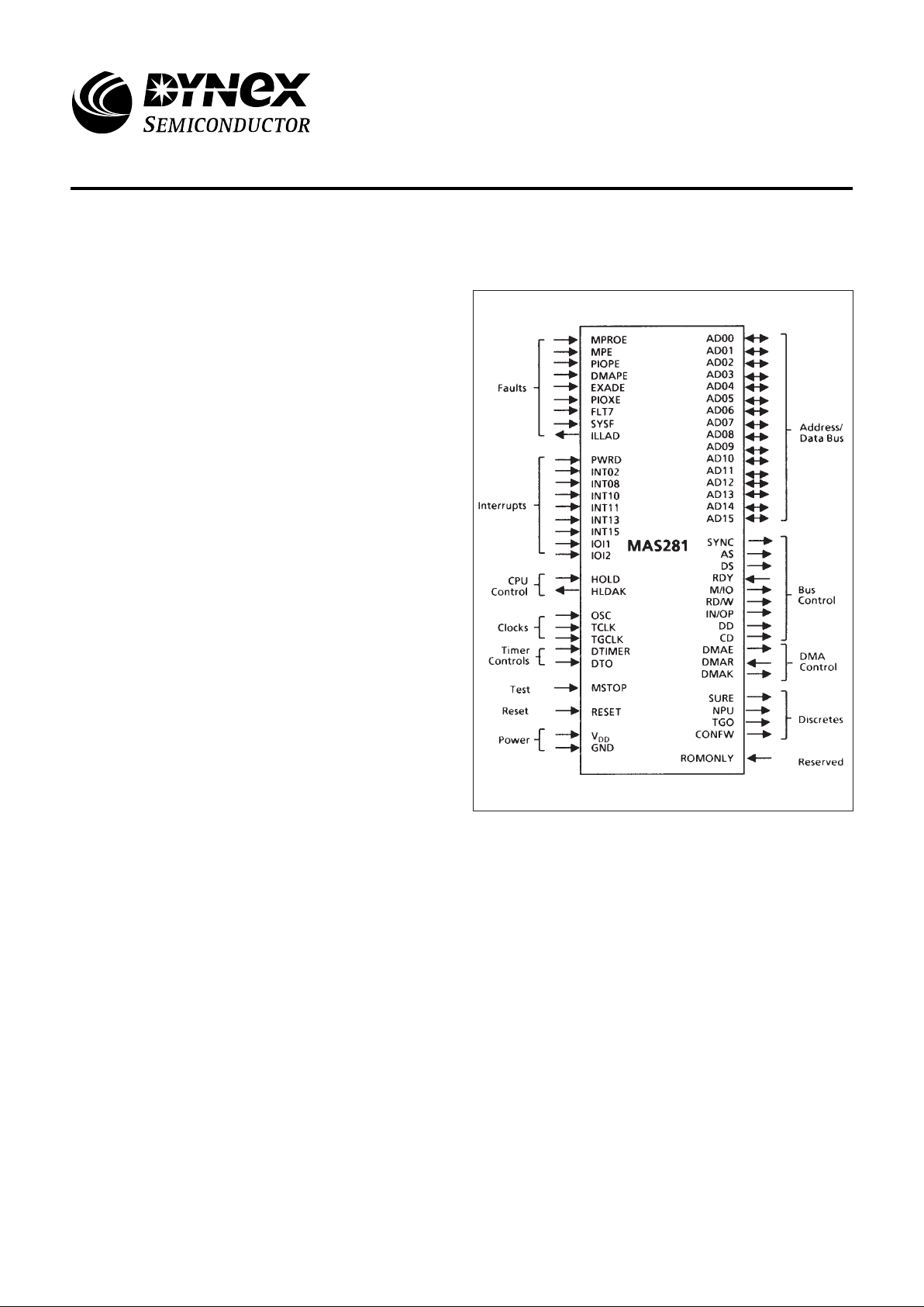
BLOCK DIAGRAM
FEATURES
■ MIL-STD-1750A 16-Bit Microprocessor
■ Full Performance over Military Temperature Range
(-55°C to + 125°C)
■ Radiation Hard CMOS/SOS Technology
■ Performance Optimised Architecture
- Parallel Multiplier/Accumulator
- 32-bit Barrel Shifter
- Instruction Pre-Fetch
- Multi-Port Register File
■ Implements MlL-STD-1750AOptions
- Timers A and B
- Trigger-Go Counter
- Start-Up ROM Interface
■ 64 K-word Address Space Expandable to 1 M-word with
Optional MMU
MAS281
MIL-STD-1750A Microprocessor
Replaces June 1999 version, DS3563-4.0 DS3563-5.0 January 2000
Page 2
MAS281
2/55
1.0 ARCHITECTURE
The MAS281 Microprocessor is a high performance
implementation of the MIL-STD-1750A (Notice 1) instruction
set architecture. It consists of three custom CMOS/SOS Large
Scale Integration chips referred to as the Execution Unit,
Control Unit, and Interrupt Unit - mounted on, and
interconnected within, a 64-pin, dual in-line ceramic substrate.
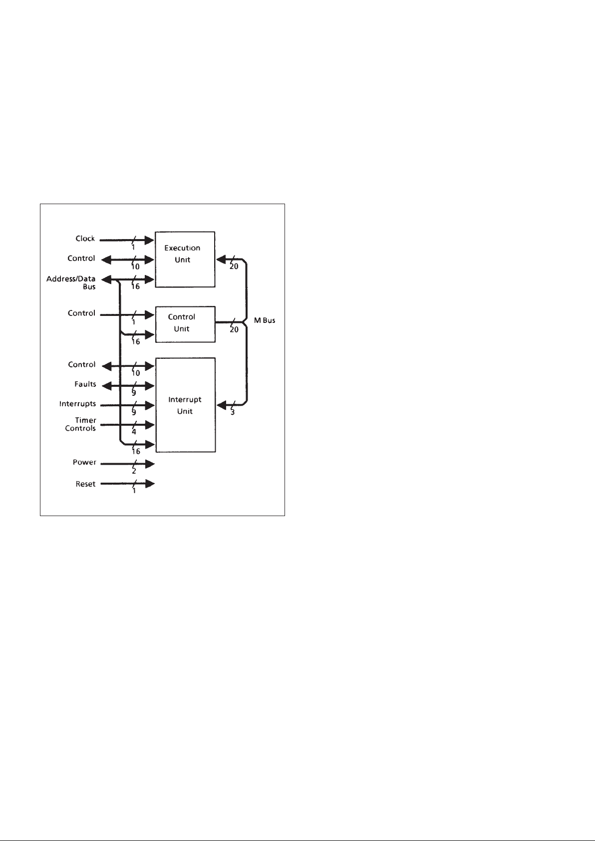
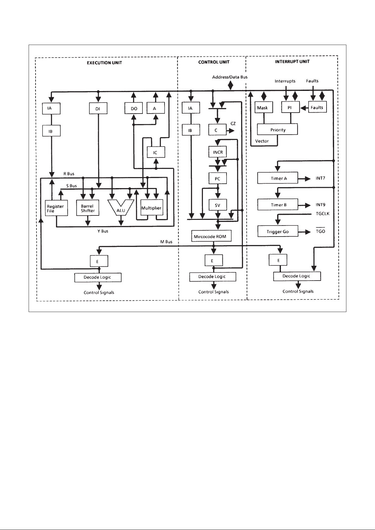
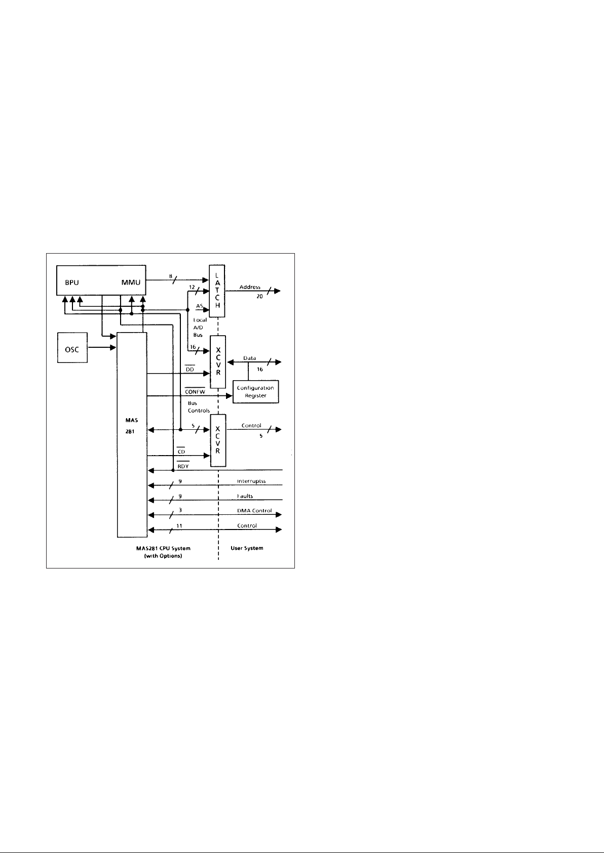
Figure 1 depicts the interconnection of these chips via the
substrate while Figure 2 depicts the architectural details within
each chip.
The MAS281 architecture has been optimised for both real
time l/O and arithmetic intensive operations. Two key features
of this architecture which contribute to the overall high
performance of the MAS281 are; a barrel shifter and a parallel
multiplier/accumulator. These subsystems allow the MAS281
to perform multi-bit shifts, multiplications, divisions, and
normalisations in a fraction of the clock cycles required on
machines not having such resources. This is especially true of
floating-point operations, in which the MAS281 excels. Such
operations constitute 16% of the Digital Avionics Instruction
Set (DAIS) mix and a generally much higher percentage of
many signal processing algorithms, therefore having a
significant impact on system performance.
In accordance with MIL-STD-1750A, the MAS281 can
access a 64K-word address space. With the addition of an
external MA31751 chip configured as a Memory Management
Unit (MMU), this address space may be expanded to a full
1Mword. Furthermore, this configuration provides write and
access lock and key protection down to 4K-word blocks. By
also configuring the MA31751 as a Block Protect Unit (BPU),
write protection may be extended down to 1K-word blocks. For
those applications not requiring adherence to the address
space requirements of MIL-STD-1750A, the MAS281 may be
optionally configured with up to 1Mword each of instruction
and operand space.
In addition to implementing all of the required features of
MIL-STD-1750A, the MAS281 also incorporates a number of
optional features. Interval timers A and B as well as a triggergo counter are provided. Most specified XIO commands are
decoded directly on the module and an additional set of
commands, associated with MMU and BPU operations, are
directly decoded on the MA31751 chip. Those commands not
directly decoded are output for decoding by external logic in
accordance with the XIO and VIO protocols of MIL-STD1750A.
1.1 EXECUTION UNIT (EU)
The EU provides the computational resources for the
MAS281. Key features include: (1) a three-bus (R, S, and Y)
data path consisting of an arithmetic/logic unit (ALU), threeport register file, barrel shifter, parallel multiplier/accumulator,
and status register; (2) instruction fetch registers IC, IA, and IB;
(3) operand transfer registers A, Dl, and DO; (4) a state
sequencer; and (5) microinstruction decode logic. A brief
description of these features follows:
1.1.1 ARITHMETIC/LOGIC UNIT (ALU)
A full function 16-bit ALU is used to perform arithmetic and
logic operations on one or two 16-bit operands in a single
machine cycle. The ALU supports 16-bit fixed-point singleprecision, 32-bit fixed-point double-precision, 32-bit floatingpoint, and 48-bit floating-point extended precision data in two’s
complement form. The ALU generates several machine flags
which reflect the outcome of its operations. These flags are
stored in the condition status (CS) field of the status register.
1.1.2 THREE PORT REGISTER FILE
A 24-word by 16-bit wide register file is used to store
operands, addresses, base pointers, stack pointers, indexes,
and temporary values. Registers R0 through R15 are general
purpose and user accessible in accordance with MIL-STD1750A; remaining registers are accessible only by microcode.
Wrap-around concatenation of R0 through R15 allows 32- and
48-bit operands to be stored. The three-port architecture
allows two 16-bit operands to be read and a third 16-bit
operand to be written simultaneously.
Figure 1: MAS281 Microprocessor Block Diagram
Page 3
MAS281
3/55
Figure 2: MAS281 Architecture
1.1.3 PARALLEL MULTIPLIER/ACCUMULATOR
This multiplies a 24-bit multiplicand by a 4-bit multiplier and
accumulates the product in a single machine cycle. Only four
iterations through the multiplier are required to complete a 16bit by 16-bit multiply.
1.1.4 BARREL SHIFTER
This shifter is a 32-bit input, 16-bit output right-shift
network. The barrel shifter allows multibit shifts to be
accomplished in a single machine cycle and is used by the
microcode for all shift, rotate, and normalise operations.
1.1.5 STATUS REGISTER
This 16-bit register holds the condition status (CS) bits C,
P, Z, and N; the 4-bit address state (AS) field; and the 4bit
processor state (PS) field. The CS bits are updated after each
logical, shift, and arithmetic operation performed by the ALU.
The CU interrogates these bits during conditional
operations to determine which course of action to follow. The
AS field is used during expanded memory access to define the
page register set to be used for instruction and operand
memory references. The PS field is used during memory
protect operations to define the access key used for memory
accesses. The PS field is also used during execution of
privileged instructions. PS must be zero for such operations to
be legal. Figure 3 depicts the status register format
1.1.6 STATE SEQUENCER
The EU utilises a state machine, clocked by the system
oscillator, to generate processor timing and control signals.
These signals constitute the lowest level of control available
within the module, and provide the framework for basic
operations, such as selecting the next microinstruction to be
executed, sequencing bus control signals to effect a memory
transfer, or performing an operation within the ALU. Each
complete pass through the state machine corresponds to one
such operation and constitutes a machine cycle.
Page 4

MAS281
4/55
1.1.7 OPERAND TRANSFER REGISTERS
The Address (A), Data In (Dl), and Data Out (DO) registers
serve to buffer transfers between the data path and the
Address/Data (AD) bus. These registers are used under
microcode control and are not directly accessible by software.
A description of the use of these registers during memory and
l/O operations is provided in section 3.0.
1.1.8 INSTRUCTION FETCH REGISTERS
The Instruction Counter (IC), Instruction A (IA), and
Instruction B (IB) registers allow sequential instruction fetches
to be performed without the assistance of the ALU. The IC
register, which holds a 16-bit address and points to the next
instruction to be fetched, is loaded indirectly via reset, jump, or
branch operations. Once loaded, it uses a dedicated counter to
sequence from one instruction to the next. IA and IB serve as
an instruction pipeline with IA storing the next instruction to be
executed. Dl also plays a role by storing any immediate
operands. Use of these registers during instruction fetches is
described in section 3.0.
1.1.9 MICROCODE CONTROL LOGIC
All EU operations are performed under microcode control.
As depicted in Figure 2, microinstructions are provided by the
CU over the M bus, buffered by the Execution (E) register, and
decoded to generate various control signals.
1.2 CONTROL UNIT (CU)
The CU provides microprogrammed control of all MAS281
operations. It features a microsequencer, a microcode storage
ROM, and an instruction mapping ROM. A brief description of
these features follows:
1.2.1 MICROSEQUENCER
This 12-bit wide microcode address generator controls all
microcode ROM accesses. The microsequencer features a
program counter (PC) which points to the next sequential
microinstruction, a program counter save register (SV) to save
return addresses for microsubroutines, address increment
logic (INCR), instruction pipeline registers (IA and IB), a next
address multiplexer, a loop counter (C), and various
miscellaneous systems.
The microsequencer controls the execution of each
MILSTD-1750A, or macro, instruction by stepping through its
corresponding microcode sequence. If the macroinstruction is
a conditional, the CS bits of the status word will be interrogated
to determine the necessary course of action. At the completion
of each macroinstruction, the microsequencer checks to see if
a Hold request or an interrupt is pending. If so, the
microsequencer will branch to the appropriate microinstruction
sequence. If not, the microsequencer begins sequencing the
next macroinstruction.
Note that the microsequencer is itself under the control of
the EU state sequencer. Each processor machine cycle
corresponds to the execution of a single microinstruction.
A machine cycle requires five or more oscillator cycles
with the exact number determined by the type of operation
being performed. Internal processor operations, excluding
internally decoded XIO commands, require either five or six
oscillator cycles, the former associated with sequential
microcode execution and the latter with microcode branches.
Internally decoded XIO commands require a minimum of six
oscillator cycles to complete. External processor operations
require a minimum of five oscillator cycles to complete.
The internal ready signal is generated by the IU whenever
an internally decoded XIO command is detected An external
ready interface is provided which allows external machine
cycles to be extended when interfacing with slow devices. The
external ready signal is provided by external logic and must be
asserted in order to conclude the machine cycle.
Field Bits Description
CS CONDITION STATUS:
0 C- Carry from an
addition or no borrow from
a subtraction
1 P- Result >0
2 Z- Result = 0
3 N- Result<0
R 4 - 7 RESERVED
PS 8 - 11 PROCESSOR STATE:
(a)- Memory access key
code
(b)- Privileged instruction
enable
AS 12 - 15 ADDRESS STATE:
Page register sets for
expanded memory
addressing
Figure 3: Status Word Format
CS R PS AS
3 4 7 8 11 12 150
Page 5

MAS281
5/55
or more faults in FT will cause a level 1 (machine error)
interrupt request. Once a fault is set in FT, it may only be
cleared via an XIO command.
1.3.5 TIMERS A AND B
These are two 16-bit software controllable timers. Timer A
is clocked by the TCLK input while Timer B is clocked by the
internally generated TCLK/10. Timers A and B will generate
interrupt levels 7 and 9, respectively, when their maximum
counts of 65,536 are reached.
1.3.6 TRIGGER-GO COUNTER
This 16-bit counter is clocked by the TGCLK input, is
enabled during system initialisation, and may be reset but not
stopped by software action. It is stopped, however, upon
overflow or by assertion of the DTIMERN input. Upon overflow,
the TGON discrete output goes low and stays low until the
counter is reset by software. This counter is typically used as a
system “watchdog" timer.
1.3.7 XIO COMMAND DECODE LOGIC
This logic decodes all internally supported XlO commands
and generates the control signals necessary to carry out the
commanded action. An internal ready signal is generated upon
command detection and is used by the EU state sequencer as
previously discussed. Table 7b in Section 4.0 identifies the XlO
commands which are internally supported by the MAS281.
1.3.8 MICROCODE CONTROL LOGIC
Decode logic, which translates microcode received from
the CU into control signals, is used both by the MAS281 and by
the external system.
2.0 INTERFACE SIGNALS
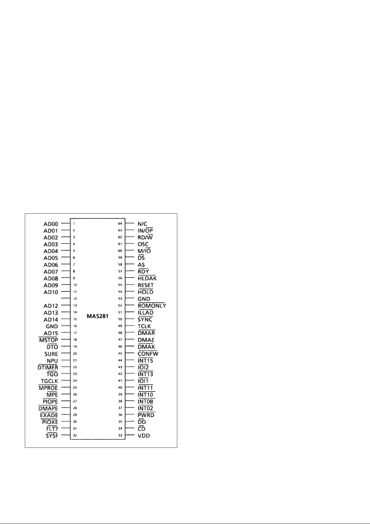
2.1 PIN ASSIGNMENTS
Figure 4 defines the pin assignment for the MAS281
module. See section 10.0 for full packaging and pin
assignment information.
All signals - with the exception of power, ground and
ROMONLYN - are TTL compatible. In addition, each function
is provided with Electrostatic Discharge (ESD) protection
circuitry. Figure 5 depicts a typical system implementation
using many of these signals. Throughout this data sheet,
active low signals are denoted either by placing a bar over the
signal name, or by following the signal name with an “N” suffix,
e.g., DDN. If a signal has a dual function, both function names
will be used separated by a “/”. The function name to the left of
the “/” will be active high while the function to the right will be
active low, again with an “N" suffix, e g., RD/WN.
1.2.2 MICROCODE ROM
This is a 2k- (2048) word by 40-bits/word ROM which
stores the microinstructions that implement the MIL-STD1750A instruction set. The address of the next microinstruction
to be accessed is generated by the microsequencer. The
accessed microinstruction is output to the M-bus and
broadcast to the EU and IU. In addition to the microinstruction
sequences corresponding to the MIL-STD-1750A instructions,
the microcode ROM also stores sequences for performing
initialisation, interrupt response, Hold response, instruction
prefetch, built-intest (BIT), and BlFs.
1.2.3 INSTRUCTION MAPPING ROM
This is a 512-word by 8-bits/word ROM which is used
during microcode branches.
1.3 INTERRUPT UNIT (IU)
The IU incorporates a pending interrupt register, a mask
register, a priority encoder, a fault register, two interval timers
(A and B), a trigger-go counter, XIO command decode logic,
and microcode control logic. A brief description of these
features follows:
1.3.1 PENDING INTERRUPT REGISTER (PL)
This 16-bit register is used to capture and hold interrupts
until they can be processed by software. Pl supports three
dedicated external, six user-definable external, and seven
dedicated internal interrupts. Interrupts are captured at the
beginning of each machine cycle and are stored using a logic 1
to represent a pending interrupt. Anti-repeat logic is provided
to prevent multiple captures of the same interrupt.
1.3.2 MASK REGISTER (MK)
This 16-bit register is used to store the interrupt mask.
Interrupts are masked by ANDing each mask bit with its
corresponding Pl register bit. Interrupts which are masked will
be captured in the Pl register but will not be acted on until
unmasked. Interrupt level 0 can not be masked. A logic 0 in a
given bit position indicates that the corresponding bit in the Pl
register will be masked.
1.3.3 PRIORITY ENCODER
This encoder generates an interrupt request to the CU
whenever one or more unmasked interrupts are pending and
enabled in the Pl and encodes the highest priority unmasked
pending interrupt as a 4-bit vector. This vector is read by the
EU over the AD bus during interrupt servicing in order to create
the interrupt Linkage and Service pointers.
1.3.4 FAULT REGISTER
This 16-bit register is used to capture and hold both internal
and user implemented external faults. Faults are captured at
the beginning of each machine cycle and are stored using
positive logic, i e, a logic “1” represents a fault. Setting any one
Page 6
MAS281
6/55
2.2 PIN FUNCTIONS
A description of each pin function follows. The function
name is presented first, followed by its acronym and
description. Function type is either input, output, high
impedance (Hi-Z), or a combination thereof. Full timing
characteristics of each of the functions are shown in section
6.0.
2.2.1 POWER AND GROUND (VDD & GND)
The MAS281 utilizes a single VDD power supply. A
singlepoint ground is provided for the three chips on the
substrate and is brought out on two module pins.
2.2.2 OSCILLATOR (OSC)
This input clocks the EU state sequencer which, in turn,
generates timing and control signals for the rest of the module.
To minimize skew between OSC edges and signals derived
from OSC, and thereby optimize system performance, the
OSC rise and fall times should be minimised. It is
recommended that a clock driver with a high drive capability,
such as a 54AS244, 54ALS244 or 54HST244, be used.
2.2.3 SYNCHRONIZATION CLOCK (SYNC)
This active low output transitions from high to low to signal
the start of a new machine cycle. It should be used as a timing
reference for those operations which must be synchronized to
the basic machine cycle.
SYNCN cycles associated with external memory or l/O bus
transactions are a minimum of five OSC periods in duration
and may be extended by inserting wait states via the external
ready interface, For such cycles, a SYNCN low indicates that
either an address or XlO command is on the AD bus; a high
indicates data is on the bus. Wait states extend the high state
of SYNCN.
SYNCN cycles associated with internal CPU operations,
are either five or six OSC periods in duration. Six OSC periods
are required for machine cycles associated with microcode
branches or with the execution of internally decoded XlO
commands. Five OSC periods are required for all other internal
operations.
[Note: For modules operating at high OSC frequencies, the
internal ready logic provided on the IU may cause a wait state
to be inserted during execution of internal XlO commands.
This would result in a SYNCN cycle of seven OSC periods
duration. Though unlikely, this condition must be taken into
account in implementing an external ready interface. Refer to
the description of the Ready (RDYN) signal below for further
details.]
SYNCN continues to cycle during DMA and HOLD states.
Such cycles are five OSC periods in duration.
2.2.4 ADDRESS STROBE (AS)
Output/Hi-Z. This active high signal indicates that an
address has been placed on the AD bus. This address is
guaranteed valid at the high to low transition of AS. AS should
be used to strobe an address latch during AD bus
demultiplexing. This latch should be a transparent type for
optimum performance. AS is placed in the high impedance
state during DMA and Hold cycles and is held low during
internal (non-XIO) operations.
2.2.5 DATA STROBE (DS)
Output/Hi-Z. This active low signal indicates that the AD
bus is being used for data transfers. During read operations,
DSN should be used by the selected external device to enable
data onto the AD bus. This data is guaranteed valid on the low
to high transition of DSN. The selected external device should
use the low to high edge of DSN to perform the write. DSN is
placed in the high impedance state during DMA and Hold
cycles and is held high during internal (nonXlO) operations.
2.2.6 READ/WRITE (RD/W)
Output/Hi-Z, This dual function signal indicates the
direction of data flow on the AD bus. A high level indicates a
read operation with data being input to the module. A low level
indicates a write operation with data being output by the
module. RD/WN may be combined with DSN to generate
separate read and write strobes. This signal goes valid shortly
Figure 4: Pin Assignments
AD11
Page 7
MAS281
7/55
after SYNCN goes low to indicate the start of a new machine
cycle and remains valid until a new SYNCN cycle is begun,
RD/WN is placed in the high impedance state during DMA and
Hold cycles.
2.2.7 MEMORY/INPUT-OUTPUT (M/IO)
Output/Hi-Z, This dual function signal indicates the type of
transfer of the AD bus that is occurring. A high state identifies
memory transfers. A low state identifies l/O transfers. M/ION
goes valid shortly after SYNCN goes low to indicate the start of
a new machine cycle and remains valid until a new SYNCN
cycle is begun. M/ION is placed in the high impedance state
during DMA and Hold cycles and is held high during internal
(non-XIO) operations.
2.2.9 ADDRESS/DATA BUS (AD00 - AD15)
Input/Output/Hi-Z. AD00 through AD15 comprise a
bidirectional multiplexed address and data bus which serves
both as the communication path between the external system
and module as well as the communication path among the
three chips on the module. It is important to note that the AD
bus is shared between the external system and internal
module resources. To avoid bus contention during internal
operations, the AD bus must be isolated from the external
system through the use of a bus transceiver. A data direction
signal (DDN) is provided for transceiver control .
Addresses, data and commands appearing on the AD bus
are represented in positive logic. A high level indicates a logic
1 and a low level indicates a logic 0. AD00 is the most
significant bit position whilst AD15 is the least significant bit
position. The AD bus is placed in the high impedance state
during the data portion of a read SYNCN cycle as well as
during DMA and Hold cycles.
2.2.10 READY (RDY)
This asynchronous active low input is used by the EU state
sequencer, in conjunction with the internal ready signal, to
determine when the current machine cycle may be completed.
By holding RDYN high, wait states may be inserted, stretching
out the current machine cycle and allowing slower devices
sufficient time to complete their operations.
[Note: If RDYN is held high during two consecutive TCLK
high-to-low transitions (with DSN low), a bus timeout fault will
occur and will be indicated in the appropriate bit in the fault
register. The occurrence of this fault will cause the EU state
sequencer to terminate the current machine cycle, drop
SYNCN low, and begin a new machine cycle. Also, the
presently executing macroinstruction will be aborted and
execution will branch, unless masked, to the machine error
interrupt (level 1) software routine. The DTON signal may be
used to override this feature.]
2.2.11 CONTROL DIRECTION (CD)
This active low output goes high to indicate the module is
driving the AS, DSN, M/ION, RD/WN and IN/OPN signals.
During DMA and Hold cycles, this signal goes low to indicate
the module has relinquished control of these signals and has
placed them in the high impedance state. The DMA or Console
controller, respectively, may then drive these signals. This
signal should be used to control the transfer direction of the
control signal transceiver.
2.2.12 DATA DIRECTION (DD)
This active low signal indicates the direction of data
transfer on the AD bus. This signal goes high to indicate a write
transfer from the module to the external system. It also goes
high during all internal module operations. DDN goes low to
indicate a read transfer from the external system to the
module. It also goes low during DMA and Hold cycles as well
as during configuration register reads.
[Note: In addition to going high during the execution of
internally implemented XIO commands, DDN also goes high
2.2.8 INSTRUCTION/OPERAND (IN/OP)
Output/Hi-Z. This dual function signal indicates the type of
data on the AD bus during the data portion of a SYNCN cycle.
A high state identifies an instruction while a low state identifies
an operand. IN/OPN goes valid shortly after SYNCN goes low
to indicate the start of a new SYNCN cycle and remains valid
until a new SYNCN cycle is begun. This signal is required
during expanded memory accesses. IN/OPN is placed in the
high impedance state during DMA and Hold cycles.
Figure 5: Typical MAS281/MA31751 System Interface
Page 8

MAS281
8/55
2.2.18 SYSTEM RESET (RESET)
This asynchronous active high input should be raised high
to reset the module. The high-to-low transition of this input will
start the module’s initialization.
2.2.19 START-UP ROM ENABLE (SURE)
This active high output goes high during initialization and
may also be asserted by software with the ESUR XIO
command. This signal remains high until removed by software
via the DSUR XIO command. When a Start-Up ROM is
present, this signal should be used to qualify its chip select or
output enable input such that the ROM may be accessed only
when SURE is high.
[NOTE: Instruction pipelining must be considered in
transitioning from Start-Up ROM to RAM when using the
DSUR XIO command. If a system overlays RAM with the StartUp ROM and transitions to execution from RAM by simply
executing DSUR from the ROM, then IA will contain the value
stored in the ROM location immediately following DSUR. This
value will be treated as an instruction and the module will
attempt to execute it. In such cases, it is recommended that
DSUR be followed by an unconditional branch instruction with
offset, i e, the BR instruction. An alternative approach is simply
to jump to a portion of RAM not overlaid by the Start-Up ROM
and execute DSUR from RAM.]
2.2.20 CONFIGURATION WORD (CONFW)
This active low output goes low when the module reads the
external configuration register and should be used as that
register’s output enable strobe (see Section 6.0). Table 1
defines the required format of the configuration register. A zero
in a given bit position indicates the specified device is present.
Bits 0 through 11 are not used by the module.
The configuration register is read during initialization to
determine the system configuration. It is also read whenever a
(BPT) instruction is executed to determine the presence of a
Console. If a console is not present, a BPT will be interpreted
as a NOP. DDN goes low during a configuration register read.
Thus, the configuration register must reside on the system AD
bus rather than the local AD bus (see Figure 5).
2.2.21 NORMAL POWER UP (NPU)
This active high output is dropped low during module
initialization as the first step of BIT. If BIT is successful, NPU
goes high and remains high until reset by software via the RNS
XIO command. NPU cannot be set high by software.
2.2.22 TIMER CLOCK (TCLK)
This clock input is used by interval timers A and B as well
as the interface fault timer. Timer A is clocked at the TCLK
frequency while timer B is clocked at a frequency of TCLK/10.
MIL-STD-1750A requires that this input be a 100kHz pulse
train.
during execution of XIO commands which are implemented in
the MA31751 MMU(BPU) chip.
If an MA31751 is used with the MAS281, it must reside on
the MAS281 local AD bus rather than the system buses (see
Figure 5). Table 7b in Section 4.0 identifies those XIO
commands which are implemented in the MA31751].
2.2.13 DIRECT MEMORY ACCESS ENABLE (DMAE)
This active high output goes high in response to the DMAE
XIO command. A high state indicates DMA requests will be
acknowledged; a low state indicates a DMA request will be
ignored.
2.2.14 DIRECT MEMORY ACCESS REQUEST (DMAR)
A low on this asynchronous active low input will cause the
processor to suspend internal operations at the end of the
current machine cycle. This request will only be acknowledged
by the module when DMAE is high.
2.2.15 DIRECT MEMORY ACCESS ACKNOWLEDGE
(DMAK)
This active low signal goes low in response to a DMA
request if DMAE is high. A low state grants use of the system
busses to the requesting DMA device by placing the module’s
AD bus, AS, DSN,RD/WN, M/ION and IN/OPN drivers into the
high impedance state and by pulling CDN and DDN low. The
high-to-low transition is synchronized to the falling edge of
SYNCN to ensure that the current machine cycle is completed
before the DMA device is granted the bus. DMAKN will remain
low until the requesting device raises DMARN.
2.2.16 HOLD REQUEST (HOLD)
A low on this asynchronous active low input will cause the
module to suspend internal processor functions at the end of
the currently executing MIL-STD-1750A instruction. A Hold
state is also entered if the processor encounters a breakpoint
(BPT) instruction and the configuration word indicates the
presence of a Console (bit 15 = 0).
[Note: Hold should be syncronised to the AS signal.]
2.2.17 HOLD ACKNOWLEDGE (HLDAK)
This active low output goes low either upon completion of
the MIL-STD-1750A instruction during which HOLDN went low
or if the processor encounters a breakpoint (BPT) instruction
with Console present indicated in the configuration word
register. A low on this signal indicates to the requesting device
that that the module AD bus, AS, DSN, M/ION, RD/WN, and
IN/OPN drivers have been placed in the high impedance state.
The Hold state is terminated either by raising HOLDN high or,
in the case of a BPT caused Hold, by pulsing HOLDN low and
high again (see Section 6.0).
Page 9

MAS281
9/55
2.2.23 TRIGGER-GO CLOCK (TGCLK)
This clock input is used by the internal 16-bit trigger-go
counter. The trigger-go counter counts at the same frequency
as TGCLK.
2.2.24 TRIGGER-GO DISCRETE (TGO)
This active low output goes low whenever the trigger-go
counter overflows, i e., the counter rolls over to 0000. It returns
to the high state when the trigger-go counter is reset by
software via the GO XIO command.
2.2.25 DISABLE TIMER (DTIMER)
A low on this active low input disables timers A and B as
well as the trigger-go counter. A low also disables DMA access
by forcing DMAE low and DMAKN high. Raising DTIMERN
allows timers A and B and the trigger-go counter to resume
counting from the value at which they were stopped. A high
also allows normal DMA operation.
2.2.26 DISABLE TIMEOUT (DTO)
A low on this active low input will reset and disable the bus
fault timeout circuitry.
2.2.27 POWER DOWN INTERRUPT (PWRD)
A low on this active low input is captured in the Pl register
by a SYNCN high-to-low transition. This sets pending interrupt
0. This is the highest priority interrupt and cannot be masked or
disabled.
2.2.28 USER INTERRUPTS (INT02,08,10,11,13 AND 15)
A low on any of these active low inputs will be captured in
the Pl register by a SYNCN high-to-low transition and will set
pending interrupt levels 2, 8, 10, 11, 13, and 15, respectively.
Level 2 is the highest priority user level while level 15 is the
lowest priority. These interrupts are maskable and can be
disabled. Unused inputs should be pulled up to VDD.
[NOTE: The INTO2 service routine should clear the PI
Register using the RPI 0002 instruction.]
2.2.29 I/0 DEDICATED INTERRUPTS (IOI1 & IOI2)
A low on either IOI1N or IOI2N will be captured in the Pl
register by a SYNCN high-to-low transition and will set pending
interrupt levels 12 and 14, respectively. Unused inputs should
be pulled up to VDD.
[NOTE: Interrupt levels 1, 3, 4, 5, 6, 7, and 9 are dedicated
to internal machine interrupts.]
2.2.30 MEMORY PROTECT ERROR (MPROE)
A low on this active low input, captured by the SYNCN
high-to-low transition, is used to inform the module that an
access fault, execute protect, or write protect violation has
been detected. Bit O of the module Fault Register (FT) is set if
this signal goes low during a memory cycle; bit 1 is set if it goes
low during a DMA cycle. Either condition immediately sets
pending interrupt level 1 and in the case of a memory cycle
error, causes the currently executing MIL-STD-1750A
instruction to be aborted.
Although the MAS281 aborts the macroinstruction, system
memory management, and / or block protect hardware is
responsible for preventing the erroneous bus cycle from
accessing memory. To effectively use this feature, MPROEN
should be pulled low prior to the high-to-low SYNCN transition
of the next machine cycle. This can easily be accomplished by
injecting wait states to hold off the DSN rising edge (write
cycle) and the SYNCN falling edge (read cycle) until the
system protection circuitry can decide whether or not to allow
the transaction.
2.2.31 MEMORY PARITY ERROR (MPE)
A low on this active low input, captured by the SYNCN
high-to-low transition, is used to inform the module that a parity
error has been detected during a memory transfer. Bit 2 of the
module Fault Register (FT) is set when this signal goes low.
This, in turn, causes pending interrupt level 1 to be set.
2.2.32 PROGRAMMED I/O PARITY ERROR (PIOPE)
A low on this active low input, captured by the SYNCN
high-to-low transition, is used to inform the module that a parity
error has been detected during an external l/O transfer. Bit 3 of
the module Fault Register (FT) is set when this signal goes
low. This, in turn, causes pending interrupt level 1 to be set.
2.2.33 DMA PARITY ERROR (DMAPE)
A low on this active low input, captured by the SYNCN
high-to-low transition, is used to inform the module that a parity
error has been detected during a DMA data transfer. Bit 4 of
the module Fault Register (FT) is set when this signal goes low
This, in turn, causes pending interrupt level 1 to be set.
2.2.34 EXTERNAL ADDRESS ERROR (EXADE)
A low on this active low input, captured by the SYNCN
high-to-low transition, is used to inform the module that a
system address error has been detected. Bit 8 of the module
Fault Register (FT) is set when this signal goes low during a
Bit Device
15 Console
14 MMU
13 BPU
12 Output Discrete Register
11-0 Unused
Table 1: Configuration Register Bit Assignment
Page 10

MAS281
10/55
memory fault; bit 5 is set if it goes low during an l/O fault. As
with MPROEN, either condition immediately sets pending
interrupt level 1 and causes the currently executing MIL-STD1750A instruction to be aborted .
2.2.35 PROGRAMMED I/O TRANSFER ERROR (PIOXE)
A low on this active low input, captured by the SYNCN
high-to-low transition, is used to inform the module that a
programmed l/O data transfer error has been detected. Bit 6 of
the module Fault Register (FT) is set when this signal goes
low. This, in turn, causes pending interrupt level 1 to be set.
2.2.36 FAULT #7 (FLT7)
A low on this active low input, captured by the SYNCN
high-to-low transition, sets bit 7 of the Fault Register (FT). This
is a user definable fault.
2.2.37 SYSTEM FAULT (SYSF)
A low on this active low input, captured by the SYNCN
high-to-low transition, sets bits 13 and 15 of the Fault Register
(FT). This is a user definable fault.
2.2.38 ILLEGAL ADDRESS (ILLAD)
This active low output drops low if the EXADEN input drops
low or if the bus fault timeout circuit causes an interface
timeout.
2.2.39 MICROCODE STOP (MSTOP)
MSTOPN allows microcode to be single-stepped and is
reserved for use by GEC Plessey Semiconductors. MSTOPN
must be pulled up to VDD in customer applications.
2.2.40 ROM ONLY (ROMONLY)
ROMONLYN is used for testing by GEC Plessey
Semiconductors and must be pulled up to VDD in customer
applications.
3.0 OPERATING MODES
MAS281 operating modes include: (1) initialisation, (2)
instruction execution, (3) interrupt servicing, (4) fault servicing,
(5) DMA support, (6) Hold support, and (7) timer operations.
3.1 INITIALISATION
The module executes a microcoded initialisation routine in
response to a hardware reset. This routine clears module
registers, disables and masks interrupts, reads the
configuration register, resets the output discrete register (if
implemented), initialises the MMU and BPU (if implemented),
performs Built-ln-Test (BIT), raises the Start-Up ROM enable
discrete, clears and starts timers A and B, resets the trigger-go
counter, and loads the instruction pipeline. Table 2
summarises the resulting initialisation state, and Table 3
provides a detailed breakdown of the initialisation sequence.
BIT consists of five subroutines, as outlined in table 4, and
begins by pulling NPU low. This is the first time after reset that
NPU is guaranteed low. If all five subroutines execute
successfully, NPU is raised high. If any part of BIT fails, an
error code identifying the failed subroutine is loaded into the
Fault Register (FT), BIT is aborted, and NPU is left in the low
state. Table 4 defines the coding of BIT results in FT. In the
event of such a failure, the resulting module reset state will be
dependent on where in BIT the error occurred and may not be
the same as that shown in Table 2. A BIT failure indication in
FT will set the level 1 interrupt request bit of the Pending
Interrupt (Pl) register. Since initialisation disables and masks
interrupts, this interrupt request will not be asserted .
The last action performed by the initialisation routine is to
load the instruction pipeline. Instruction fetches start at
memory location zero and will be from the Start-Up ROM if
implemented. Whether BIT passes or not, the processor will
begin instruction execution at this point.The system start-up
code may include a routine to enable and unmask interrupts in
order to detect and respond to a BIT failure.
[NOTE: To complete initialisation and pass BIT, interrupt
and fault inputs must be high for the duration of the
initialisation routine. Also, timers A and B must be clocked
during this interval, i.e., TCLK must be applied.]
MAS281
Instruction Counter (IC) Zeroed
Status Word (EU and MMU) (SW) Zeroed
Fault (FT) Zeroed
Pending Interrupt (PI) Zeroed
Mask (MK) Zeroed
Interrupts Disabled
DMA Access Disabled
Timer A Reset and Started
Timer B Reset and Started
Trigger-Go Timer Reset and Started
MMU
Page Registers Group 0 Enabled
AL, W, E Fields Zeroed
PPA Field Logical to Physical
Map
BPU
Write Protect Zeroed
Global Memory Protect Enabled
Table 2: Initialisation State
Page 11

MAS281
11/55
Label Cycle
MAIN B 1 1. Enable Control of DMAE Output signal
P 2. B1 3. Clear MAS281 Execution Unit Status Word (SW)
Clear Interrupt Mask (MK) (Internal l/O command, SKM 2000H)
B1 4. Clear Pending Interrupt Register (Pl) and Fault Register (FT) (Internal l/O Command, CLIR,2001 H)
Clear Instruction Counter (IC)
P 5. B1 6. Disable Interrupts (Internal l/O Command, DSBL,2003H)
P 7. B1 8. Clear MMU Status Word (Internal l/O Command, WSW, 200EH) (Note 1)
P 9. B1 10. Disable DMA Access (lnternal l/O Command, DMAD, 4007H)
P 11. B1 12. Read Configuration Register (Internal l/O Command, RCW, 8400H, CONFWN Drops low per Figure 25,
Section 5.0)
P 13. P 14. B2 15. - (If Output Discrete Register Present, then Continue; Else, Skip to 18.)
P (16). I/O (17). Clear Output Discrete Register (External l/O Command)
P 18. B2 19. - (If BPU present, then Branch to BPU; else, continue)
P 20. B2 21. - (If MMU present, then Branch to MMU, Else, Continue)
P 22. - (Setup Temporary Register to indicate No MMU Present)
B2 23. - (Branch to MAS281 BIT)
P 24. B1 25 Enable Start-Up ROM (Internal l/O Command, ESUR,4004H; SURE Raises High per Figure 25,
Section 5.0)
P 26. B1 27. Clear and Start Timer A (Internal l/O Command, OTA,400AH)
B1 28. Reset the Trigger-Go timer (mternal l/O Command, GO,400BH)
P 29. B1 30. Clear and Start Timer B (Internal l/O Command, OTB,400EH)
B2 31. - (Branch to Load Instruction Pipeline Routine)
M 32. Load data-ln register (Dl) and instruction Register A (IA) from [IC] Increment IC
M 33. Load Data-ln Register (Dl) and Instruction Register a (IA) from [IC] ([lA] Moves to IB), Increment IC,
Map Instruction Register B (IB) into Mlcrocode Routine
BPU P (1). -
P (2). - (Set Loop to Clear Memory Protect RAM)
I/O (3). Clear a Location in MPRAM (Internal l/O Command, LMP,50XXH), Increment Address, Do 128 Times
(4). - (Branch Back to 20 )
MMU P (1). -
P (2). P (3). - (Setup Loop to Load Instructlon Page Registers (IPR) and Operand Page Registers (OPR) with
Sequential Values of 0 to 255)
P (4). P (5). I/O (6). Load a Location in the IPR wlth the value of the Location Address (Internal l/O Command, WIPR,
51 XYH)
I/O (7). Load a Location in the OPR Increment Loaded Value with the Value of the Location Address (Internal
I/O Command. WOPR,52XYH)
P (8). - (Increment IPR Address)
P (9). - (Increment OPR Address- Repeat Loop 14 - 9 1256 Times)
B2 (10). - (Setup Temporary Register to Indlcate MMU Present; Branch back to 23)
Notes:
1. This operation is performed whether or not an MMU is present.
2. “-” indicates internal CPU operation
3. Sequence numbers in “( )” are performed only under the stated conditions.
4. Each step enumerated above represents a single machine (SYNC) cycle of the type shown in the “Cycle” column.
“P” indicates a 5 OSC cycle,60% duty cycle, machine cycle.
“I/O” and “M” Indicate a 5 OSC cycle,50% duty cycle, machine cycle.
“B1” indicates a 6 OSC cycle 50% duty cycle machine cycle.
“B2” indicates a 6 OSC cycle 66% duty cycle machine cycle
Table 3: MAS281 Initialisation Sequence
Page 12

MAS281
12/55
3.2 INSTRUCTION EXECUTION
Once initialisation has been completed, the module will
begin instruction execution. Instruction execution is
characterised by a variety of operations, each one or more
machine cycles in duration. Depending on the instruction
being executed at the time, these operations include: (1)
internal CPU cycles, (2) instruction fetches, (3) operand
transfers, and (4) input/output transfers. Instruction execution
may be interrupted at the end of any individual machine cycle
by DMA operations and at the conclusion of any given
instruction by an interrupt or Hold request.
3.2.1 INTERNAL CPU CYCLES
Internal CPU cycles are used to perform all CPU data
manipulation and housekeeping operations. Internal CPU
cycles are either five or six oscillator periods in duration and
are characterised by AS low and DSN, DDN and M/ION high.
Section 6.0 provides timing characteristics for internal CPU
cycles. Tables 7a and 7b in Section 4.0 provide machine cycle
counts (both the five and the six OSC cycle variety) associated
with each MIL-STD-1750A instruction.
3.2.2 INSTRUCTION FETCHES
Instruction Fetches are used to keep the instruction
pipeline full. This ensures that the next instruction is always
ready for execution when the preceding instruction is
completed. During jump and branch instruction execution, the
pipeline is flushed, and then it is refilled via two consecutive
instruction fetches starting at the new instruction location. The
pipeline is also refilled as part of interrupt and hold request
processing.
Instruction fetches are characterised by IN/OPN high but
are otherwise identical to an operand read transfer. For a
detailed explanation of the function of various bus control
signals during instruction fetches, refer to the discussion of
operand transfers below. Section 6.0 provides timing
characteristics for instruction fetches. Machine cycles
associated with instruction fetches are a minimum of five
oscillator periods in duration. The RDYN signal may be used to
insert wait states to accommodate slow memory. Machine
cycle counts included in Table 7a of Section 4.0 include
instruction fetches.
Instruction fetches use instruction pipeline registers IA and
IB, the instruction counter (IC), and the data input register (Dl)
and proceed as follows: assuming an empty instruction
pipeline (occurring as a result of a reset, jump, or branch), the
contents of IC are placed on the AD bus as an address. The
returned value, which will be an instruction, is stored in the IA
register.
The value in IC is incremented (via its dedicated counter)
and the next fetch is performed. This second returned value,
which may be either an instruction or an immediate operand, is
stored in both the IA and Dl registers. The instruction
previously stored in IA is advanced to IB to be executed.
The instruction in IB is checked to determine if an
immediate operand is required. If so, that operand has already
been pre-fetched and resides in both IA and Dl. If not, then the
value currently in IA is an instruction. If IA contains an operand,
another instruction fetch is performed and the returned value is
stored only in IA (the contents of IB and Dl are preserved). If IA
contains an instruction, however, the next fetch is deferred
until the contents of IB are no longer needed. At that time, the
deferred fetch is performed, IA is advanced to IB for execution,
and the newly returned value is stored in both IA and Dl.
This sequence repeats until the instruction pipeline is again
emptied at which time the whole process is repeated .
3.2.3 OPERAND TRANSFERS
Operand transfers are used to obtain (read in) operands to
be used by an instruction and to save (write out) any results of
an instruction’s execution. Section 6.0 provides timing
characteristics for operand transfers. Machine cycles
associated with operand transfers are a minimum of five
oscillator periods in duration. The RDYN signal may be used to
insert wait states to accommodate slow memory. Machine
cycle counts in Table 7a of Section 4.0 include operand
transfers.
Operand transfers use the address register (A), the data
input register (Dl), and data output register (DO). Before the
operand transfer begins, the processor calculates the effective
operand address and stores this value in A. For write transfers,
the processor loads the operand into the DO register.
All operand transfers between the module and memory
are referenced to the AS and DSN bus control signals and are
characterised by IN/OPN low and, by M/ION and CDN high.
The transfer begins by placing the contents of A (the address
register) on the AD bus immediately following the SYNCN
high-to-low transition. The AS strobe then goes high to enable
the system’s transparent address latch. The address is
assured valid on the high-to-low transition of AS. The DDN
signal is high during the address portion of the transfer; its
subsequent action depends on whether the transfer is a read
or write.The RDWN signal indicates the direction of the
transfer. If the operand is a write, the address from A is
replaced by the operand in DO when SYNCN transitions from
low-to-high. Next, the DSN signal goes low and can be used by
the memory system to generate a write enable. Data is
guaranteed valid at the low-to-high transition of DSN. DDN
stays high for the duration of a write transfer. The memory
system must pull RDYN low to conclude the transfer.
If the operand transfer is a read, the AD bus drivers are
placed in a high impedance state at the low-to-high transition
of SYNCN to give the memory system access to the bus. Next,
the DSN signal goes low and can be used by the memory
system to generate an output enable. Shortly after DSN goes
low, DDN also goes low. This should be used by the system to
reverse the direction of the system’s AD bus transceivers. The
memory system must pull RDYN low to conclude the transfer.
Data will be read into the Dl register on the SYNCN high-to-low
transition 3.2.4 Input/Output Transfers
Input/Output transfers utilize the MIL-STD-1750A XIO and
VIO protocols and are characterized by M/ION and IN/OPN
low and CDN high. RD/WN defines the direction of the
transfer. AS and DSN cycle as with operand transfer
operations. The procedure followed depends on whether the
transfer is associated with one of the internally implemented
XIO commands or an externally implemented capability. An
exception is the Read Configuration Word (RCW) command
Page 13

MAS281
13/55
which is decoded by the MAS281 but is treated, in some ways,
like an externally implemented XIO command. This exception
is discussed below.
Internal l/O transfers involve all XIO commands which are
decoded internally either by the MAS281 or by the MA31751
MMU/BPU chip (with the exception noted above). Table 7b
identifies these commands. The A, Dl and DO registers are
used as in operand transfers. Internal l/O transfers are
characterised by DDN staying high for the duration of the
transfer in order to prevent bus contention between the module
AD bus and the system bus. Machine cycle associated with
internal I/O commands are normally six oscillator cycles in
duration but might be extended to seven OSC cycles by the
internal ready interface if the module is run at high frequencies.
Internal I/O transfers may be subdivided into writes, reads and
commands as follows:
I/O writes consist of a command phase followed by the
value to be written. The command is placed on the AD bus
from the A register at the SYNCN high-to-low transition and is
assured valid on the high-to-low transition of AS. The value to
be written is placed on the AD bus from the DO register at the
SYNCN low-to-high transition and is written to the internal l/O
device by the subsequent SYNCN high-to-low transition. An
example of an internal l/O write is loading timer A.
I/O reads consist of a command phase followed by the
value returned by the internal device. The command is placed
on the AD bus from the A register at the SYNCN high-to-low
transition and is assured valid on the highto-low transition of
AS. The internal l/O device places the value to be read on the
AD bus at the SYNCN low-tohigh transition. This value is
captured by the Dl register on the subsequent SYNCN high-tolow transition. An example of such an operation is reading the
interrupt mask register.
I/O commands consist of a command phase alone. The
command is placed on the AD bus from the A register at the
SYNCN high-to-low transition and is executed at the following
SYNCN high-to-low transition. An example of an l/O command
is raising the DMAE discrete.
External l/O transfers are similar to internal l/O transfers
with the following exceptions: (1) DDN goes low, as with
operand transfers, during an l/O read; and (2) external l/O
machine cycles are normally five OSC cycles in duration and
may be extended via the RDYN signal as with operand
transfers.
As discussed earlier, the Read Configuration Word
command is a special case. It is decoded internally to generate
a read strobe (CONFWN) and therefore uses both the
standard internal I/O six OSC period machine cycle as well as
the internal ready interface to extend its cycle. It relies on an
externally implemented configuration register, however, and
therefore cycles DDN as with external I/O cycles. Therefore,
the configuration word register must reside on the system side
of the data bus transceivers as opposed to residing directly on
the local AD bus (as shown in Figure 5).
Nine user interrupt request inputs are provided for
programmed response to asynchronous system events. A low
on any of these inputs will be detected at the high-to-low
transition of SYNCN and latched into the Pending Interrupt (Pl)
BIT Test Coverage BIT Fail Codes (FT 13,14,15) Cycles
1 Microcode Sequencer
IB Register Control 100 220
Barrel Shifter
Byte Operations and Flags
2 Temporary Registers (T0 - T7)
Microcode Flags 101 165
Multiply
Divide
3 Interrupt Unit- MK, Pl, FT 111 216
Enable/Disable Interrupts
4 Status Word Control
User Flags 110 155
General Registers (R0 - R15)
5 Timer A 111 775
Timer B
- BIT Pass/Fail Overhead - 25
Note: BIT pass is indicated by all zeros in FT bits 13,14, and 15.
Table 4: Built-in Test Coverage and Tuning
Page 14
MAS281
14/55
LP SP
Interrupt Address Address
PWRD 0 20 21
12223
INT02 2 24 25
32627
42829
52A2B
62C2D
72E2 F
INT08 8 30 31
93233
INT10 10 34 35
INT11 11 36 37
IOI1 12 38 39
INT13 13 3A 3B
IOI2 14 3C 3D
INT15 15 3E 3F
Table 5: Interrupt Pointer Definitions
Figure 6: Interrupt Vectoring
interrupts are output to the priority encoder where the highest
priority is encoded as a 4-bit vector. If interrupts are enabled,
and an unmasked interrupt is pending, the priority encoder will
assert an interrupt request to the CU.
Upon completing execution of a given MIL-STD-1750A
instruction, the CU’s microsequencer checks the state of the
priority encoder’s interrupt request. If an interrupt request is
asserted, the microsequencer branches to the microcode
interrupt service routine. This routine performs a read of the
priority encoder’s 4-bit pending interrupt vector, stores the
value in the EU Dl register, and then uses this value to
calculate the appropriate interrupt linkage and service
pointers. The pointers serve as addresses to data structures
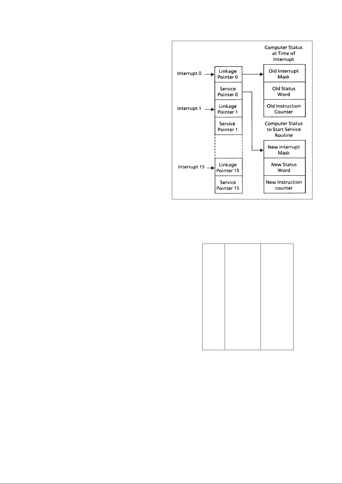
used in servicing interrupts. Figure 6 depicts this relationship.
Table 5 defines pointer values.
Using the linkage and service pointers, the microcode
interrupt service routine performs the following: (1) the current
contents of the status word, mask register, and instruction
counter are saved; (2) a write status word l/O command is
executed with an all zero data word; (3) the new mask is
loaded into MK and interrupts are disabled; (4) the new status
word is read and checked for a valid AS field - If AS is non-zero
and an MMU is not present, AS is set to zero and fault 11
(address state error) is set in the fault register FT; (5) a write
status word command using the new status word is performed;
and (6) the new IC value is loaded into IC, the instruction
pipeline is filled starting at the new address, and instruction
execution begins.
[NOTE: The steps listed above represent a summary of
actions performed during interrupt servicing and do not
necessarily reflect the actual order in which these events take
place.]
If an interrupt is latched during the interrupt service routine,
it will not be processed until interrupts are re-enabled. If an AS
fault occurs during the service routine, interrupt level 1 will be
set. This interrupt will be serviced when interrupts are reenabled unless it is masked by the new value in MK.
3.4 FAULT SERVICING
Eight user fault inputs are provided. A low on any of these
inputs will be latched into the Fault Register (FT) at the high-tolow transition of SYNCN.
register on the following SYNC high-to-low transition (with the
exception of INT02N which is latched into Pl when INT02N is
first detected). This sequence occurs whether interrupts are
enabled or disabled or whether the specific interrupt is masked
or unmasked.
Each external Pl register input is buffered by a falling edge
detector to prevent repeat latching of requests held low
beyond the first SYNCN high-to-low transition. An interrupt
request input must transition to the high state before a
subsequent request on that input will be detected.
When an interrupt request is latched into Pl, it is ANDed
with its corresponding mask bit in the mask register (MK).
Interrupt level 0 is not maskable. Any unmasked pending
Page 15

MAS281
15/55
No falling edge detectors are provided to prevent repeat
latching of faults held low beyond the first SYNCN high-to-low
transition. However, all FT bits are ORed together and input to
the Pl bit 1 through an edge detector to prevent the fault
register from causing multiple level 1 interrupts.
The sequence of events following a fault capture depends
on the type of fault as follows:
3.4.1 MPEN, PIOPEN, DMAPEN, PIOXEN, FLT7N, AND
SYSFN
The capture of one or more of these faults immediately sets
pending interrupt level 1 (machine error) of the Pending
Interrupt (Pl) register. Anti-repeat logic between the FT and Pl
prevents latching more than a single interrupt into the Pl before
the user interrupt service routine has cleared the FT. The
microcoded interrupt service routine reads the interrupt priority
vector from the Interrupt Unit and clears the service interrupt
from the Pl. At this point the Pl is ready to latch another
interrupt into this bit.
When this microcoded service routine acts on a level 1
interrupt, it clears the Pl bit 1, but the FT maintains the
interrupting bit(s). Therefore, a level 1 interrupt would be
latched again if there was no anti-repeat logic to prevent a
never-ending loop of interrupts.
During the SYNCN cycles between fault capture and the
beginning of the microcode interrupt handling routine, AS and
DSN are forced to their inactive states. In the case of
MPROEN, which may reflect an attempted write violation, it is
required that system hardware provide the additional
protection necessary to inhibit memory write strobe.
Interrupts are serviced at the end of the currently executing
instruction if not masked and if interrupts are enabled. System
software servicing level 1 interrupts must clear the FT via the
RCFR internal l/O command at some point in the routine to
allow subsequent faults to latch a level 1 interrupt request. A
non-destructive read of the FT is provided by the internal l/O
command RFR, but this command should be used carefully.
3.4.2 MPROEN, EXADEN, AND BUS FAULT TIME-OUT
The capture of one or more of these faults immediately sets
pending interrupt level 1 (machine error) of the Pending
Interrupt (Pl) register. Furthermore, the instruction currently
executing is aborted at the SYNCN high-to-low transition
following the SYNCN high-to-low transition that latched the
fault. The IC value saved in the interrupt linkage table for the
level 1 interrupt always points to the instruction which was in
instruction pipeline register IA at the time of the abort. Antirepeat logic between the FT and Pl prevents latching more
than a single interrupt into the Pl before the user interrupt
service routine has cleared the FT.
The microcoded interrupt service routine reads the
interrupt priority vector from the Interrupt Unit and clears the
serviced interrupt from the Pl. At this point the Pl is ready to
latch another interrupt into this bit. When this microcoded
service routine acts on a level 1 interrupt, it clears the Pl bit 1,
but the FT maintains the interrupting fault bit(s). Therefore, a
level 1 interrupt would be latched again if there were no antirepeat logic to prevent a never-ending loop of interrupts from
occurring .
3.5 DMASUPPORT
DMA data transfers are performed under the control of a
system DMA controller over the system AD bus. The user
signals that DMA requests will be honored by setting the
DMAE output high via the DMAE internal XlO command. The
DMA controller may request use of the AD bus by pulling the
module’s DMARN input low.
Unless the DMAE output is high, all such requests will be
ignored. If DMAE is high, DMARN will be acknowledged by
DMAKN dropping low. This occurs at the first SYNCN high-tolow transition after DMARN goes low.
DMAKN low indicates that the module has relinquished
control of the AD bus by placing its AD bus, AS, DSN, M/ION,
RD/WN and IN/OPN drivers in their high impedance state.
DDN is dropped low to direct the system data bus transceivers
to drive the local AD bus and CDN is dropped low to disable
the control signal buffers. The DMA controller relinquishes
control of the AD bus by raising DMARN high. The module
responds by raising DMAKN high at the next SYNCN high-tolow transition and continuing with program execution.
3.6 HOLD SUPPORT
The Hold state is provided to facilitate debugging of user
software by allowing the user to disable the MAS281 and
access system resources. Hold state timings is defined in
Section 6.0. The Hold state can be entered either by pulling
HOLDN low or by executing a BPT instruction with the Console
present and indicated in the Configuration Word. These two
approaches, as well as methods for using the Hold state to
single step through software, are discussed below:
3.6.1 USING HOLDN
At the completion of the currently executing instruction, the
microsequencer checks the state of the HOLDN input. If low,
the microsequencer branches to the microcode Hold service
routine. This routine decrements IC twice, enables the Hold
termination sequence, drops HLDAKN low, and enters the
Hold state. HLDAKN drops low three SYNCN cycles after the
final SYNCN cycle of the currently executing instruction. A low
on HLDAKN indicates that the module has relinquished the AD
bus by placing its AD bus, AS, DSN, M/ION, RD/WN and IN/
OPN drivers into the high impedance state and, DDN and CDN
drop low.
When HOLDN is returned high, the Hold state will end on
the subsequent high-to-low transition of SYNCN. This is
signified by raising HLDAKN, at which point thc module
resumes control of the AD bus, AS, DSN, M/ION, RD/WN and
IN/OPN signals. CDN and DDN raise high.Thc instruction
pipeline is then refilled and instruction execution resumes with
the first instruction loaded into the pipeline
Page 16
MAS281
16/55
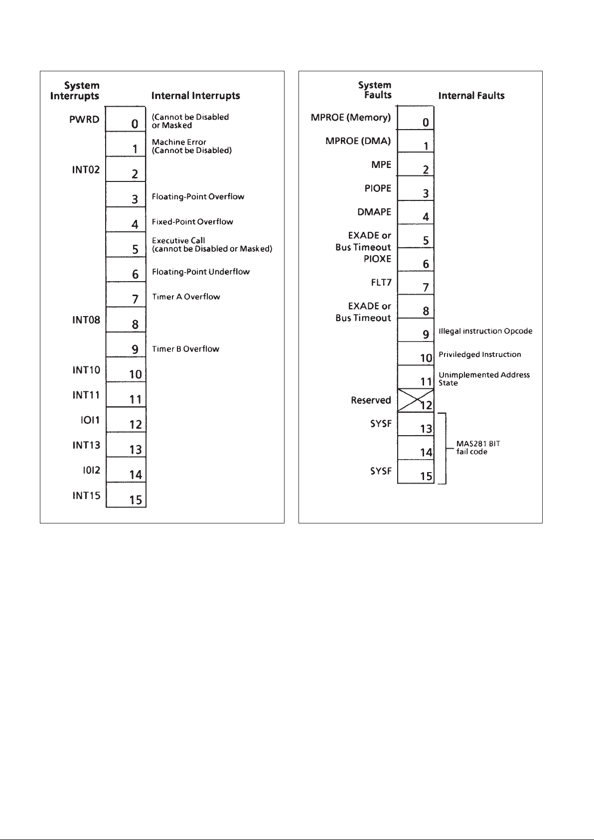
Figure 7: Pending Interrupt Register Bit Assignments
Figure 8: Fault Register Bit Assignments
3.6.2 USING BPT
The Hold state may also be entered by executing a BPT
instruction with Console present indicated in the Configuration
Word. On encountering a BPT instruction, the processor reads
the Configuration Word to check for the presence of a
Console. If a Console is indicated, the microsequencer
branches to the microcode BPT Hold service routine. This
routine decrements IC once, drops HLDAKN low, and enters
the Hold state.
To release the MAS281 from a BPT initiated Hold state, the
HOLDN input must be pulsed low in accordance with the
timing diagrams in Section 6.0. When HOLDN returns high, the
Hold state will be released on the following SYNCN high-to-low
transition. The instruction pipeline is then refilled and
instruction execution resumes with the first instruction loaded
into the pipeline.
3.6.3 SINGLE-STEPPING
Software can be single-stepped through the proper use of
the HOLDN input and the BPT instruction. Use the BPT
instruction to mark the beginning of the section of code which
will be stepped through. Pulse HOLDN low to release the BPT
initiated Hold state and then pull HOLDN low again during the
two subsequent SYNCN cycles that refill the instruction
pipeline. When the first instruction following Hold release
completes execution, the module will once again enter the
Page 17

MAS281
17/55
l/O) of the Fault Register (FT) is set. This sets pending
interrupt level 1 and causes the current bus cycle to be
terminated by forcing SYNCN low. The MIL-STD-1750A
instruction is aborted, and control passes to the level 1
interrupt service routine (if the level 1 interrupt is unmasked).
This feature is disabled by pulling DTON low.
4. SOFTWARE CONSIDERATIONS
The MAS281 implements the full MIL-STD-1750A
instruction set. Table 7a lists the instruction set and provides
performance data for each instruction. Table 7b provides a
summary of the XIO commands which are internally decoded
on the module. Resources available to the software
programmer are depicted in Figure 9. A discussion of data
types, addressing modes and benchmarking considerations
follows.
4.1 DATA TYPES
The MAS281 fully supports 16-bit fixed-point single
precision, 32-bit fixed-point double-precision, 32-bit floatingpoint, and 48-bit extended precision floating point data types.
Figure 10 depicts the formats of these data types.
All numerical data is represented in two’s complement
form. Floating-point numbers are represented by a fractional
two’s complement mantissa with an 8-bit two’s complement
exponent. All floating-point operands are expected to be
normalized. If not normalized, the results from an instruction
are not defined.
4.2 ADDRESSING MODES
The MAS281 supports the eight addressing modes
specified in MIL-STD-1750A. These addressing modes are
depicted in Figure 11 and are defined below.
4.2.1 REGISTER DIRECT (R)
The register specified by the instruction contains the
required operand.
4.2.2 MEMORY DIRECT (D,DX)
Memory Direct (without indexing) is an addressing mode in
which the instruction contains the memory address of the
required operand. In Memory Direct-lndexed (DX), the
memory address of the required operand is specified by the
sum of the contents of an index register (RX) and the
instruction address field (A). Register R1 through R15 may be
specified for indexing.
4.2.3 MEMORY INDIRECT (I, IX)
Memory Indirect (without indexing) is an addressing mode
in which the memory address specified by the instruction
contains the address of the required operand. In Memory
Indirect with Pre-lndexing (IX), the sum of the contents of a
specified index register and the instruction address field in the
address that contains the address of the required operand.
Registers R1 through R15 may be specified for pre-indexing.
Hold state. Again pulling HOLDN will cause the next instruction
to execute. This process may be repeated as long as required.
Raising HOLDN high will resume normal operatlon.
3.7 TIMER OPERATIONS
The MAS281 implements interval timers A and B, a trigger-
go counter, and a bus fault timer. A discussion of each follows:
3.7.1 TIMERS A AND B
Timer A is clocked by the TCLK input; timer B is clocked by
an internally generated TCLK/10. MIL-STD-1750A requires
TCLK to be a 100-kHz pulse train. If allowed to overflow, timers
A and B will set level 7 and level 9 interrupt requests,
respectively. Timing characteristics of each timer are defined
in Section 5.0. Either timer can be read, loaded, started, and
stopped through the use of internally decoded XIO commands.
These commands are identified in Table 7b in Section 4.0.
By asserting the DTIMERN input, both timers will halt and all
internally decoded XIO commands which would change their
state are disabled (asserting DTIMERN also disables DMA
accesses by driving DMAE low and DMAKN high). Raising
DTIMERN allows the timers to resume counting from their
suspended state and allows timer commands to function
normally (DMA control lines are again allowed to change).
A feature of the MAS281 timers is the choice of disabling,
or not disabling, the interval timers A and B upon execution of
a BPT software instruction when a Console is connected. If full
compliance with MIL-STD-1750 (Notice 1) is desired, the
halting of timers A and B can be accomplished by pulling
DTIMERN low upon execution of a BPT instruction with a
Console connected. Two suggested ways to do this are: (1)
connect HLDAKN to DTIMERN through an AND gate; or (2)
allow the system Console to pull DTIMERN low upon receiving
HLDAKN low. The first option provides a faster response and
is a less complicated method, whereas the second choice
allows the option of halting timers A and B, or not halting them.
[NOTE: As described in Section 2.2, DTIMERN low
suspends the trigger-go timer and disables DMA access
(forces DMAE low and DMAKN high) in addition to halting
timers A and B].
3.7.2 TRIGGER-GO COUNTER
The trigger-go counter is clocked by the TGCLK input.
Timing characteristics for trigger-go counter operation are
defined in Section 6 0. DTIMERN disables and enables
operation in the same manner as with timers A and B.
Whenever the trigger-go counter overflows, TGON drops low
and remains low until the counter is reset via the GO internal
XIO command.
3.7.3 BUS FAULT TIMER
All bus operations are monitored to ensure timely
completion. A hardware timeout circuit is enabled at the start of
each memory and l/O transfer (DSN high-to-low transition) and
is reset upon receipt of the external ready (RDYN) signal.
If this circuit fails to reset within a minimum of one TCLK
period or a maximum of two TCLK periods, either bit 8 (if the
transaction is with memory) or bit 5 (if the transaction is with
Page 18

MAS281
18/55
Figure 9: Register Set Model
Figure 10: Data Formats
4.2.4 IMMEDIATE LONG (IM, IMX)
There are two formats which implement Immediate Long
Addressing; one allows indexing and one does not. For the
indexable form, if the specified index register, RX, is not equal
to zero, the contents of RX are added to the immediate field to
form the required operand; otherwise, the immediate field
contains the required operand.
4.2.5 IMMEDIATE SHORT (IS)
In this mode the required 4-bit operand is contained within
the 16-bit instruction. The Immediate Short addressing mode
accommodates two formats; one which interprets the contents
of the immediate field as positive data and the other which
interprets the contents of the immediate field as a negative
data.
4.2.5.1 IMMEDIATE SHORT POSITIVE (ISP)
The immediate operand is treated as a positive integer
between 1 and 16.
4.2.5.2 IMMEDIATE SHORT NEGATIVE (ISN)
The immediate operand is treated as a negative integer
between -1 and -16. Its internal form is a two’s complement,
sign-extended 16-bit number.
4.2.6 INSTRUCTION COUNTER RELATIVE (ICR)
This addressing mode is used for 16-bit branch
instructions. The contents of the instruction counter minus two
(the address of the current instruction) is added to the sign-
Page 19

MAS281
19/55
extended 8-bit displacement field within the instruction. This
sum then points to the memory address to which control will be
transferred if the branch is taken.
4.2.7 BASE RELATIVE (B)
There are two formats which implement Base Relative
Addressing; one allows indexing and one does not. For the
non-indexable form, the contents of the instruction specified
base register (BR = BR’ + 12) is added to the 8-bit
displacement field (DU) of the 16-bit instruction. For the
indexable form, the sum of the contents of a specified index
register and a specified base register is the address of the
required operand. Registers R1 through R15 may be specified
for indexing. Registers R12 through R15 may be specified as
the base register.
4.2.8 SPECIAL
This addressing mode is applicable to instructions that do
not follow the above formats. The instructions that use this
special mode are indicated in Table 7a.
4.3 BENCHMARKING
Table 7a defines the number and type of machine cycles
associated with each MIL-STD-1750A instruction. This
information may be used when benchmarking MAS281
performance. The Digital Avionics Instruction Set (DAIS) mix,
which defines a typical frequency of occurrence for MIL-STD1750A instructions, is used here for this purpose.
One problem with the DAIS mix, however, is that it does not
reflect the impact of data dependencies on system
performance. For example, a multiplication in which an
operand is zero may be performed much faster than one with
two non-zero operands. Also, the DAIS mix does not specify
such time consuming operations as normalization and
alignment.
Realistic benchmarks must therefore take both the
instruction mix and data dependencies into account. To this
end, machine cycle counts in Table 7a which have data
dependencies, are annotated with either an "a" or "wa"suffix.
An "a" suffix reflects an average number of machine
cycles (where each of several possibilities is equally likely) and
a
“
"wa" suffix reflects a weighted average number of machine
cycles (where some data possibilities are more likely than
others).
Weighted averages are only applicable to floating-point
operations. Weighted averages provided in Table 7a are
based on the Sweeney (IBM) guidelines. These guidelines
take a wide range of data dependencies into consideration.
Normalization and alignment operations are also represented.
Table 6 defines MAS281 throughput, at various frequencies
and wait states, for the DAIS mix using Sweeney data
dependencies.
It should be noted that using the Sweeney guidelines is a
conservative approach to benchmarking. If best case
assumptions are made and such operations as normalization
and alignment are not considered, MAS281 performance
figures are approximately 50% higher than those indicated in
Table 6.
25 743.4 698.3 658.4 622.8
20 594.7 558.7 526.7 498.2
15 446.0 419.0 395.0 373.7
10 297.4 279.3 263.4 249.1
0123
Number of Wait States in Memory Access Cycle
f
OSC
MHz
Table 6: Throughput (KIPS)
Page 20

MAS281
20/55
Figure 11: Addressing Modes
Page 21

MAS281
21/55
4.4 INSTRUCTION SUMMARY
Table 7a: Instruction Summary
MPB
* M = memory, P = processor (5 OSC cycles) B = processor (6 OSC cycles),
a = average if more than one alternative exists
Cycles *
Operation Op Code/Ext Mnemonic Format
LOAD/STORE
Single Precision Load 81 LR R 1 0 0
0X LB B 2 1 0
4X 0 LBX BX 2 1 0
82 LISP ISP 1 0 0
83 LISN ISN 1 0 0
80 L D, DX 3 0 0
85 LIM IM,IMX 2 0 0
84 Ll I,IX 4 1 0
Double-Precision Load 87 DLR R 1 2 0
0X DLB B 3 1 0
4X 1 DLBX BX 3 2 0
86 DL D, DX 4 0 0
88 DLI I,IX 5 1 0
Single-Precision Store 0X STB B 2 2 0
4X 2 STBX BX 2 2 0
90 ST D, DX 3 1 0
94 STI I, IX 4 1 0
Store a Non-Negative 91 STC D,DX 3 1 0
Constant 92 STCI I, IX 4 1 0
Double-Precision Store 0X DSTB B 3 2 0
4X 3 DSTX BX 3 2 0
96 DST D DX 4 0 0
98 DSTI I, IX 5 1 0
Load Multiple Registers 89 LM D,DX 3+n 1 1
Store Multiple Registers 99 STM D,DX 3+n 1 1
INTEGER ARITHMETIC
Single-Precision Integer Add A1 AR R 1 1 0
1 X AB B 2 2 0
4X 4 ABX BX 2 2 0
A2 AISP ISP 1 1 0
A0 A D, DX 3 1 0
4A 1 AIM IM 2 1 0
Increment Memory by a A3 INCM D,DX 4 1 0
Positive Integer
Single-Precision Absolute A4 ABS R 1 1.5 1a
Value of Register
Double-Precision Absolute A5 DABS R 1 2.5 1a
Value of Register
Page 22

MAS281
22/55
Operation Op Code/Ext Mnemonic Format Cycles *
Double-Precision Integer A7 DAR R 1 3 0
Add A6 DA D, DX 4 1 0
Single Precision Integer B1 SR R 1 1 0
Subtract 1 X SBB B 2 2 0
4X 5 SBBX BX 2 2 0
B2 SISP ISP 1 1 0
B0 S D, DX 3 1 0
4A 2 SIM IM 2 1 0
Decrement Memory by a B3 DECM D,DX 4 1 0
Positive Integer
Single Precision Negate B4 NEG R 1 1 0
Register
Double-Precision Negate B5 DNEG R 1 3 0
Register
Double-Precision Integer B7 DSR R 1 3 0
Subtract B6 DS D,DX 4 1 0
Single Precision Integer C1 MSR R 1 6.5 4a
Multiply with 16-Bit Product C2 MISP ISP 1 7.5 4a
C3 MISN ISN 1 7.5 4a
C0 MS D,DX 3 6 5 4a
4A 4 MSIM IM 2 6.5 4a
Single Precision Integer C5 MR R 1 5 3
Multiply with 32-Bit Product 1X MB B 2 7 3
4X 6 MBX BX 2 7 3
C4 M D, DX 3 5 3
4A 3 MIM IM 2 5 3
Double-Precision Integer C7 DMR R 1 41 4.5a
Multiply C6 DM D,DX 4 40 4.5a
D1 DVR R 1 20.25 5.5a
Single Precision Integer D2 DISP ISP 1 20 5.5a
Divide with 16-Bit Dividend D3 DISN ISN 1 20.5 5.5a
D0 DV D,DX 3 20.25 5.5a
4A 6 DVIM IM 2 20.25 5.5a
Single Precision Integer D5 DR R 1 21.75 6.5a
Dividewith 32-Bit Dividend 1X DB R 2 22.75 6.5a
4X 7 DBX BX 2 22.75 6.5a
D4 D D,DX 3 21.75 6.5a
4A 5 DIM IM 2 22.75 6.5a
Double-Precision Integer D7 DDR R 1 79.5 5.5a
Divide D6 DD D,DX 4 77.5 5.5a
MPB
* M = memory, P = processor (5 OSC cycles), B = processor (6 OSC cycles),
a = average if more than one alternative exists
Table 7a: Insttruction Summary (continued)
Page 23

MAS281
23/55
Operation Op Code/Ext Mnemonic Format Cycles *
LOGICAL
Inclusive Logical OR E1 ORR R 1 0 0
3X ORB B 2 1 0
4X F ORBX BX 2 1 0
E0 OR D, DX 3 0 0
4A 8 ORIM IM 2 0 0
Logical AND E3 ANDR R 1 0 0
3X ANDB B 2 1 0
4X E ANDX BX 2 1 0
E2 AND D, DX 3 0 0
4A 7 ANDM IM 2 0 0
Exclusive Logical OR E5 XORR R 1 0 0
E4 XOR D, DX 3 0 0
4A 9 XORM IM 2 0 0
Logical NAND E7 NR R 1 1 0
E6 N D, DX 3 1 0
4A B NIM IM 2 1 0
Set Bit 51 SBR R 1 0 0
50 SB D, DX 4 1 0
52 SBI I, IX 5 2 0
Reset Bit 54 RBR R 1 1 0
53 RB D, DX 4 1 0
55 RBI I ,IX 5 2 0
Test Bit 57 TBR R 1 0 0
56 TB D, DX 3 0 0
58 TBI I, IX 4 1 0
Test and Set Bit 59 TSB D,DX 4 0 2
Set Variable Bit in Register 5A SVBR R 1 0 1
Reset Variable Bit in Register 5C RVBR R 1 1 1
Test Variable Bit in Register 5E TVBR R 1 0 1
Store Register Through Mask 97 SRM D,DX 4 3 0
BYTE
Load From Upper Byte 8B LUB D,DX 3 0 0
8D LUBI I,IX 4 1 0
Load From Lower Byte 8C LLB D DX 3 1 0
8E LLBI I, IX 4 2 0
Store Into Upper Byte 9B STUB D,DX 4 1 0
9D SUB I I, IX 5 3 0
Store Into Lower Byte 9C STLB D,DX 4 1 0
9E SLBI I,IX 5 2 0
Exchange Bytes in Register EC XBR S 1 0 1
* M = memory, P = processor (5 OSC cycles), B = processor (6 OSC cycles).
Table 7a: Instruction Summary (continued)
MPB
Page 24

MAS281
24/55
Operation Op Code/Ext Mnemonic Format Cycles *
COMPARE
Single-Precision Compare F1 CR R 1 0 0
3X CB B 210
4X C CBX BX 2 1 0
F2 CISP ISP 1 0 0
F3 CISN ISN 1 0 0
F0 C D, DX 3 0 0
4A A CIM IM 2 0 0
Compare Between Limits F4 CBL D,DX 4 2.75 1.75a
Double-Precision Compare F7 DCR R 1 2 0
F6 DC D, DX 4 0 0
JUMP/BRANCH
Jump on Condition 70 JC D, DX 2 0.5 1a
71 JCI I,IX 3 0 5 1a
Jump to Subroutine 72 JS D, DX 2 2 0
Subtract One and Jump 73 SOJ D, DX 2 2.5 1a
Branch Unconditionally 74 BR ICR 2 2 0
Branch if Equal to (Zero) 75 BEZ ICR 1 5 1 1a
Branch if Less than (Zero) 76 BLT ICR 1.5 1 1a
Branch to Executive 77 B EX S 16 12 3a
Branch if Less than or 78 BLE ICR 1.5 1 1a
Equal to (Zero)
Branch if Greater than (Zero) 79 BGT ICR 1.5 1 1a
Branch if Not Equal to (Zero) 7A BNZ ICR 1.5 1 1 a
Branch if Greater than or 7B BGE ICR 1.5 1 1a
Equal to (Zero)
SHIFT
Shift Left Logical 60 SLL R 1 1 0
Shift Right Logical 61 SRL R 1 1 0
Shift Right Arithmetic 62 SRA R 1 1 0
Shift Left Cyclic 63 SLC R 1 1 0
Double Shift Left Logical 65 DSLL R 1 3 0
Douible Shift Right Logical 66 DSRL R 1 2 0
Double Shift Right Arithmetic 67 DSRA R 1 2 0
Double Shift Left Cyclic 68 DSLC R 1 3 0
Shift Logical, Count in Register 6A SLR R 1 1 3
Shift Arithmetic, Count in Register 6B SAR R 1 1.5 3.50a
Shift Cyclic, Count in Register 6C SCR R 1 1 3.25a
Double Shift Logical, Count 6D DSLR R 1 2.25 4a
in Register
Double Shift Arithmetic, Count 6E DSAR R 1 3.19 4.94a
in Register
Double Shift Cyclic, Count 6F DSCR R 1 3.5 3a
in Register
* M = memory, P = processorr (5 OSC cycles), B = processor (6 OSC cycles),
a = average if more than one alternative exists.
MPB
Table 7a: Instruction Summary (continued)
Page 25

MAS281
25/55
Operation Op Code/Ext Mnemonic Format Cycles *
CONVERT
Convert Floating-Point to 16-Bit E8 FIX R 1 4.25 4.5a
Integer
Convert 16-Bit Integer to Floating- E9 FLT R 1 3 2a
Point
Convert Extended-Precision EA EFIX R 1 12.25 6.25a
Floating-Point to 32-Bit Integer
Convert 32-Bit Integer to EB EFLT R 1 7.5 3.5a
Extended-Precision Floating-Point
STACK
Stack IC and Jump to Subroutine 7E SJS D, DX 4 3 0
Unstack IC and return from
Subroutine 7F URS S 3 1 1
Pop Multiple registers off the
Stack 8F POPM S 2.5+n 2.25+n 4.25a
(n=O to 15) (n=O to 15)
Push Multiple Registers on to the
Stack 9F PSHM S 1 + n 4.5 + n 2a
(n=O to 15) (n=O to 15)
I/O (See l/O Command Summary)
Execute l/O 48 XlO** IM,IMX 3 3.583 6.277a
Vectored l/O 49 VlO** D,DX - - -
SPECIAL
Built-ln Function Call 4F BIF S
Move Multiple Words, Memory-to- 93 MOV S 1+4n 1+3n 1+2na
Memory
Exchange Words in Registers ED XWR R 1 2 0
Load Status 7D LST** D, DX 8 2 3
7C LSTI** I, IX 9 2 4
No Operation FF NOP S 1 2 2
Break Point FF BPT S 3 4 4
* M = memory, P = processor (5 OSC cycles), B = processor (6 OSC cycles),
a = average if more than one alternative exists
** Priveleged instruction
MPB
Table 7a: Instruction Summary (continued)
Page 26

MAS281
26/55
Operation Op Code/Ext Mnemonic Format Cycles *
FLOATING-POINT
Extended-Precision Floating- 8A EFL D, DX 5 0 1
Point Load
Extended-Precision Floating- 9A EFST D, DX 5 0 1
Point Store
Floating-Point Absolute Value AC FABS R 1 1.75 3.25a
of Register
Floating-Point Negate Register BC FNEG R 1 3.25 3.75a
Floating-Point Compare F9 FCR R 1 2.75 2.875wa
3X FCB B 2 2.75 2.875wa
4X D FCBX BX 2 2.75 2.875wa
F8 FC D, DX 3 1.75 2.875wa
Extended-Precision Floating- FB EFCR R 1 3.25 2.875wa
Point Compare FA EFC D,DX 4.25a 2.75 2.875wa
Floating-Point Add A9 FAR R 1 7.625 8.25wa
2X FAB B 3 6.625 8.25wa
4X 8 FABX BX 3 6.625 8.25wa
A8 FA D, DX 4 5.625 8.25wa
Extended-Precision Floating- AB EFAR R 1 21.3125 10.5625wa
Point Add AA EFA D, DX 5 19.3125 10.5625wa
Floating-Point Subtract B9 FSR R 1 8.625 8.625wa
2X FSB B 3 7.625 8.625wa
4X 9 FSBX BX 3 7.625 8.625wa
B8 FS D, DX 4 6.625 8.625wa
Extended-Precision Floating- BB EFSR R 1 23.0625 11.8125wa
Point Subtract BA EFS D, DX 5 21.0625 11.8125wa
Floating-Point Multiply C9 FMR R 1 12.75a 6.25wa
2X FMB B 3 12.75a 6.25wa
4X A FMBX BX 3 12.75a 6.25wa
C8 FM D, DX 4 11.75a 6.25wa
Extended-Precision Floating- CB EFMR R 1 59.75 6.25wa
point Multiply CA EFM D, DX 5 57.75 6.25wa
Floating-Point Divide D9 FDR R 1 31.5 32.75wa
2X FDB B 3 30 5 32.75wa
4X B FDBX BX 3 30 5 32.75wa
D8 FD D, DX 4 29.5 32.75wa
Extended-Precision Floating- DB EFDR R 1 102.625 47.875wa
Point Divide DA EFD D, DX 5 100.625 47 875wa
* M = memory, P = processor (5 OSC cycles), B = processor (6 OSC cycles),
a = average if more than one alternative exists
wa = weighted average favouring one or more possible alternatives
MP B
Table 7a: Instruction Summary (continued)
Page 27

MAS281
27/55
4.5 INTERNAL I/O COMMAND SUMMARY
Operation Command Mnemonic Cycles *
Implemented in MAS281
Set Fault Register 0401 SFR 2 3 9
Set Interrupt Mask 2000 SMK 2 3 9
Clear Interrupt request 2001 CLIR 2 3 9
Enable Interrupts 2002 ENBL 2 3 9
Disable Interrupts 2003 DSBL 2 3 9
Reset Pending Interrupt 2004 RPI 2 3 9
Set Pending Interrupt Register 2005 SPI 2 3 9
Reset Normal Power Up Discrete 200A RNS 2 3 9
Write Status Word 200E WSW 2 3a 8.5a
Enable Start-Up ROM 4004 ESUR 2 3 9
Disable Start-Up ROM 4005 DSUR 2 3 9
Direct Memory Access Enable 4006 DMAE 2 3 9
Direct Memory Access Disable 4007 DMAD 2 3 9
Timer A Start 4008 TAS 2 3 9
Ti mer A Halt 4009 TAH 2 3 9
Output Timer A 400A OTA 2 3 9
Reset Trigger-Go 400B GO 2 3 9
Timer B Start 400C TBS 2 3 9
Timer B Halt 400D TBH 2 3 9
Output Timer B 400E OTB 2 3 9
Read Configuration Word 8400 RCW 2 2 4
Read Fault Register Without Clear 8401 RFR 2 2 4
Read Interrupt Mask A000 RMK 2 2 4
Read Pending Interrupt Register A004 RPIR 2 2 4
Read Status Word A00E RSW 2 1 4
Read and Clear Fault Register A00F RCFR 2 2 4
Input Timer A C00A ITA 2 2 4
input Timer B C00E ITB 2 2 4
Implemented in BPU
Memory Protect Enable 4003 MPEN 2 4 8
Load Memory Protect RAM 50XX LMP 2 4 8
Read Memory Protect RAM D0XX RMP 2 3 3
Implemented in MMU
Write Instruction Page Register 51XY WIPR 2 4 8
Write Operand Page Register 52XY WOPR 2 4 8
Read Memory Fault Status A00D RMFS 2 3 3
Read Instruction Page Register DlXY RIPR 2 3 3
Read Operand Page Register D2XY ROPR 2 3 3
* M = memory, P = processor (5 OSC cycles), B = processor (6 OSC cycles),
a = average if more than one alternative exists
MPB
Table 7b: Internal I/O Command Summary
Page 28

MAS281
28/55
5.0 TIMING CHARACTERISTICS & DIAGRAMS
This section provides detailed timing specifications for the
MAS281, under the test loads detailed below. Cross hatching
in all figures indicates either a “don't care” or undeterminate
state.
Load 2
Load 3
*Includes all jig and parasitic capacitance
Page 29

MAS281
29/55
Figure 12: Reset Timing
Figure 13: Internal CPU Operations
Page 30

MAS281
30/55
NOTES:
1. Dashed timing lines indicate no-wait cycle timing.
2. Other output states: CD = HIGH and DMAK = HIGH
3. Other required input states: HOLD = HIGH, DMAR = HIGH and RESET = LOW.
Figure 14: Write Transfer Timing
Page 31

MAS281
31/55
NOTES:
1. Dashed timing lines indicate no-wait cycle timing.
2. Other output states: CD = HIGH, HLDAK = HIGH and DMAK = HIGH
3. Other required input states: HOLD = HIGH, DMAR = HIGH and RESET = LOW.
Figure 15: Read Transfer Timing.
Page 32

MAS281
32/55
NOTES:
1. Dashed timing lines indicate no-wait cycle timing.
2. Other output states: CD = HIGH, HLDAK = HIGH and DMAK HIGH
3. Other required input states: HOLD = HIGH, DMAR = HIGH and RESET = LOW.
Figure 16: Internal I/O Write/Command
Page 33

MAS281
33/55
NOTES:
1. Dashed timing lines indicate no-wait cycle timing.
2. Other output states: CD = HIGH, HLDAK = HIGH and DMAK HIGH
3. Other required input states: HOLD = HIGH, DMAR = HIGH and RESET = LOW.
Figure 17: Internal I/O Read Timing
Page 34

MAS281
34/55
NOTE:
Other required input states: DTIMER = HIGH and RESET = LOW
Figure 18: DMA Access/Release Timing
NOTE:
Other required input: RESET = LOW
Figure 19: Interrupt Request Timing
Page 35

MAS281
35/55
NOTES:
1. 2 TCLK falling edges during a continuous DS = low are necessary to cause a bus fault timeout.
2. Other output states: HLDAK = HIGH.
3. Other required input states: DTO = HIGH and RESET = LOW.
Figure 20: Bus Fault Timeout Timing
NOTES:
1. Assumes only one fault active at a time.
2. Buffered EXADE.
3. Other required input state: RESET = LOW.
Figure 21: Fault Capture Timing
Page 36

MAS281
36/55
NOTES:
1. The "don't care" state will continue to exist until HLDAK = HIGH, RDY will then resume normal operation.
2. HOLD falling may occur at any time during software execution. The diagram shows the last possible time it can occur
and be assured of entering the HOLD state after the current instruction completes execution.
3. Other required input states: RESET = LOW.
Figure 22: Hold State Generation Timing
Page 37

MAS281
37/55
NOTES:
1. ADDRESS = IC(BPT) initiated the Hold state.
ADDRESS = IC(Hold) - 2, if HOLD = LOW initiated the Hold state (unless changed by the monitor system).
2. Other output states: DMAK HIGH.
3. Other required input states: DMAR = HIGH and RESET = LOW.
Figure 23: Hold State Termination Timing
Page 38

MAS281
38/55
NOTES:
1. Other required input: RESET = LOW.
2. TCLK/10 is the internally derived Timer B clock.
3. Timers A and B are clocked on the second SYNC falling edge after TCLK set-up time is satisfied.
Figure 24: Timer Operations
Page 39

MAS281
39/55
NOTES:
1. Other required input states: RESET = LOW.
Figure 25: Discrete Outputs Timing
Page 40

MAS281
40/55
6.0 ABSOLUTE MAXIMUM RATINGS
Parameter Min Max Units
Supply voltage -0.5 7 V
Input voltage -0.3 VDD+0-3 V
Current through any pin -20 20 mA
Operating temperature -55 125
o
C
Storage temperature -65 150
o
C
Table 8: Absolute Maximum Ratings
Stresses above those listed may cause permanent damage to
the device. This is a stress rating only and functional operation
of the device at these conditions, or at any other condition
above those indicated in the operations section of this
specification is not implied. Exposure to absolute maximum
rating conditions for extended periods may affect device
reliabillty.
Subgroup Definition
1 Static characteristics specified in Table 9 at +25°C
2 Static characteristics specified in Table 9 at +125°C
3 Static characteristics specified in Table 9 at -55°C
7 Functional characteristics specified at +25°C
8A Functional characteristics specified at +125°C
8B Functional characteristics specified at -55°C
9 Switching characteristics specified in Table 10 at +25°C
10 Switching characteristics specified in Table 10 at +125°C
11 Switching characteristics specified in Table 10 at -55°C
DEFINITION OF SUBGROUPS
7.0 DC ELECTRICAL CHARACTERISTICS
Total Dose Radiation Not
Exceeding 3x10⁵ Rad (Si)
Symbol Parameter Condition Min. Typ. Max. Units
V
DD
Supply voltage 4.5 5.0 5.5 V
V
IH
TTL Input High Voltage 2.0 V
V
IL
TTL Input Low Voltage 0.8 V
V
CH
OSC Input High Voltage 4.0 V
V
CL
OSC Input Low Voltage 1.0 V
V
OH
TTL Output High Voltage IOH = -1.4mA 3.5 V
VDD = 4.5V
V
OL
TTL Output low Voltage lOL = 2.0mA 0.4 V
VDD = 5.5V
I
IZ
Input Leakage Current (Note 1) VDD = 5.5V ±10 µA
I
OZ
Output Leakage Current (Note 1) VDD = 5.5V ±150 µA
I
DD
Power Supply Current f = 20MHz 70 133 mA
Mil-Std-883, method 5005, subgroups 1, 2, 3
VDD = 5V±10%, over full operating temperature range
Note 1: Worst case at TA = +125°C, guaranteed but not tested at TA = -55°C
Table 9: Operating DC Electrical Characteristics
Page 41

MAS281
41/55
8.0 TIMING PARAMETERS
NO. Parameter Test Condition Min. Max. Units
(notes 1 & 9) (note 2) (note 2)
1 RESET setup to SYNC lo (note 3) - 30 ns
2 RESET hold after SYNC lo (note 3) - 15 ns
3 RESET hi to RESET lo (note 3) 2 - SYNC
4 OSC hi to SYNC lo Load 1 10 40 ns
5 OSC hi to SYNC hi Load 1 10 40 ns
6 SYNC lo to SYNC lo (notes 4 & 5) Load 1 5T - 2 5T + 2 ns
7 SYNC lo to AS hi (note 6) Load 1 1T - 10 1T + 5 ns
8 SYNC lo to AS lo Load 1 2.5T - 10 2.5T + 15 ns
9 SYNC lo to DS lo (read) Load 1 3T - 5 3T + 20 ns
10 SYNC lo to DS hi (read) Load 1 10 30 ns
11 SYNC lo to DS lo (write) Load 1 3T - 5 3T + 22 ns
12 SYNC lo to DS hi (write) (note 5) Load 1 4.5T -5 4.5T + 10 ns
13 SYNC lo to DD lo Load 1 3 T + 20 3T + 60 ns
14 SYNC lo to DD hi Load 1 20 60 ns
15 SYNC lo to Address valid Load 2 - 68 ns
16 Address valid after SYNC lo Load 2 3T + 15 - ns
17 SYNC lo to AD Bus Hi-Z (read)
(notes 7 & 10) Load 2 - 3T + 50 ns
18 SYNC lo to AD Bus active (read) (note 10) Load 2 15 - ns
19 SYNC lo to Data valid (write) Load 2 - 3T + 45 ns
20 Data valid after SYNC lo (write) Load 2 12 - ns
21 Data set up to SYNC lo (read) 20 - ns
22 Data hold after SYNC lo (read) (note 8) Load 2 0 - ns
23 SYNC lo to M/IO, RD/VV, IN/OP valid Load 1 - 70 ns
24 M/IO, RD/WN, IN/OP valid after SYNC lo Load 1 5 - ns
25 RDY setup to OSC lo 15 - ns
26 RDY hold after OSC lo 5 - ns
27 SYNC lo to DMAE valid Load 1 - 75 ns
28 DMAE valid after SYNC lo Load 1 5 - ns
29 DMAR setup to SYNC lo 20 - ns
30 DMAR hold after SYNC lo 10 - ns
NOTES:
Mil-Std-883, method 5005, subgroups 9, 10, 11
1. Unless otherwise noted, test condltions are as follows: OSC duty cycle = 50%, input rise and fall time < 5ns, timing
measured from 50% of VDD points.
2. t = 1 OSC period. 0.5t implies a 50% OSC duty cycle; fractional t’s may be adjusted to reflect actual OSC duty cycle.
3. Data obtained by characterisation or analysis, is not routinely measured.
4. Add 1t for potential branch cycle.
5. Add 1t for internal XIO cycle; nt for n memory wait states.
6. Excluding DMA or HOLD conditions.
7. Measured to pre-Hi-Z steady state ± 10% of VDD.
8. Measurement minus 1x10⁻⁷ in [1-(VlL-0 5/VDD-0.5)] nsecs.
9. Output references SYNC, DMAK, and HLDAK drive into load 1.
10. Guaranteed by component LSI testing: not measured on microprocessor module.
Table 10. Timing Parameters
Page 42

MAS281
42/55
NO. Parameter Test Condition Min. Max. Units
(notes 1 & 9) (note 2) (note 2)
31 SYNC lo to DMAK valid Load 1 - 50 ns
32 DMAK valid after SYNC lo Load 1 5 - ns
33 DMAK lo to DD lo Load 1 - 30 ns
34 DMAK hi to DD hi Load 1 - 30 ns
35 DMAK lo to CD lo Load 1 - 30 ns
36 DMAK hi to CD hi Load 1 - 30 ns
37 DMAK lo to AD Bus Hi-Z (note 7) Load 2 - 70 ns
38 DMAK hi to AD Bus valid (note 10) Load 2 - 60 ns
39 DMAK lo to AS, DS, M/IO, RD/W,
IN/OP Hi-Z (note 7) Load 2 - 50 ns
40 DMAK hi to AS, DS, M/IO,
RD/W, IN/OP valid (note 10) Load 2 - 59 ns
41 HOLD set up to SYNC lo 40 - ns
42 HOLD hold after SYNC lo 15 - SYNC
43 SYNC lo to HLDAK valid Load 1 - 20 ns
44 HLDAK valid after SYNC lo Load 1 -7 - ns
45 HLDAK lo to DD lo Load 1 - 50 ns
46 HLDAK hi to DD hi Load 1 - 50 ns
47 HLDAK lo to CD lo Load 1 - 50 ns
48 HLDAK hi to CD hi Load 1 - 50 ns
49 HLDAK lo to AD Bus Hi-Z
(Hold) (notes 7 & 10)) Load 2 - 60 ns
50 HLDAK hi to AD bus
valid (note 10) Load 2 - 50 ns
51 HLDAK to AS, DS, M/IO,
RD/W, IN/OP Hi-Z (notes 7 & 10) Load 2 - 30 ns
52 HLDAK to AS, DS, M/IO,
RD/W, IN/OP valid (note 10) Load 1 - 30 ns
53 Interrupts set up to SYNC lo 20 - ns
54 Interrupts hold after SYNC lo 10 - ns
55 Faults setup to SYNC lo 20 - ns
56 Faults hold after SYNC lo 15 - ns
57 SYNC lo to SURE, NPU valid Load 1 - 50 ns
58 SYNC hi to CONFW valid Load 1 - 75 ns
59 TCLK lo to ILLAD lo (Bus timeout)
(note 10) Load 1 - 75 ns
60 SYNC lo to ILLAD hi (Bus timeout)
(note 10) Load 1 - 75 ns
Notes:
1. Unless otherwise noted, test conditions are as follows: OSC duty cycle = 50%, input rise and fall tlme < 5ns, timing
measured from 50% of VDD points.
2. t = 1 OSC period. O 5t implies a 50% OSC duty cycle; fractional t's may be adjusted to reflect actual OSC duty cycle.
7. Measured to pre-Hi-Z steady state ±10% of VDD.
9. Output references SYNC, DMAK, and HLDAK drive into load 1.
10. Guaranteed by component LSI testing: not measured on microprocessor module.
Table 10: Timing Parameters (continued)
Page 43

MAS281
43/55
NO. Parameter Test Condition Min. Max. Units
(notes 1 & 9) (note 2) (note 2)
61 SURE, NPU, ILLAD, CONFW
valid after SYNC lo (note 10) Load 1 5 - ns
62 TGCLK lo to TGO lo (Timer clocking) (note 10) Load 1 - 150 ns
63 SYNC hi to TGO hi
(Reset Trigger-Go XIO) (note 10) Load 1 - 75 ns
64 TCLK setup to SYNC lo (note 10) 30 - ns
65 TCLK hold after SYNC lo (note 10) 10 - ns
66 DTIMER setup to SYNC lo (note 10) 50 - ns
67 DTIMER hold after SYNC lo (note 10) 10 - ns
68 DTIMER setup to TGCLK hi (note 10) 30 - ns
69 DTIMER hold after TGCLK lo (note 10) 12 - ns
70 DTO setup to TCLK lo (note 10) 30 - ns
71 DTO hold after TCLK lo (note 10) 10 - ns
72 DTIMER lo to DMAE lo (note 10) Load 1 - 60 ns
73 DTIMER hi to DMAE normal operation (note 10) Load 1 - 60 ns
74 TCLK lo to Normal operation after
bus timeout (note 10) - 100 ns
75 EXADE lo to ILLAD lo (note 10) Load 1 - 60 ns
76 EXADE hi to ILLAD hi (note 10) Load 1 - 60 ns
77 SYNC lo to DD hi (Internal to XIO) (note 3, 10) Load 1 - 60 ns
78 Bus fault timeout interval (note 3, 10) 1 2 TCLK
79 DD hi to AS lo (DMA) (note 3, 10) Load 1 20 - ns
80 DS hi to Data valid (note 10) Load 1 (DS), 15 - ns
Load 2 (Data)
Notes:
1. Unless otherwise noted, test conditions are as follows: OSC duty cycle = 50%, input rise and fall time < 5ns, timing measured
from 50% of VDD points.
2. t = 1 OSC period 0.5t implies a 50% OSC duty cycle; fractional t's may be adjusted to reflect actual OSC duty cycle
3. Data obtained by characterisation or analysis, is not routinely measured.
9. Output references SYNC, DMAK, and HLDAK drive into load 1.
10. Guaranteed by component LSI testing: not measured on microprocessor module.
Table 10: Timing Parameters (continued)
Page 44

MAS281
44/55
9.0 CHIP SET INTERCONNECTION
To form the MAS281 processor from the individual chips
MA17501, MA17502 and MA17503, connects should be made
as shown below.
Figure 26: Chip Set Interconnection Diagram
Page 45

MAS281
45/55
10.0 PACKAGING INFORMATION
DUAL-IN-LINE CERAMIC MODULE
(MAS281 - PACKAGE TYPE C)
3.200 ± 0.032
1.100
± 0.011
0.900
± 0.020
0.100
0.220 max
0.110 ± 0.010
0.280 ± 0.015
0.100 typ
Pin 1
3.100
Figure 27: Dimensioned Drawing
Page 46

MAS281
46/55
FLATPACK CERAMIC MODULE
(MAS281 - PACKAGE TYPE F)
Figure 28a: Dimensioned Drawing
1.100
± 0.011
2.100 max
0.100
Pin 1
0.220 max
3.200 ± 0.032
Dimensions in Inches
Page 47

MAS281
47/55
Figure 28b: Pin Assignment for Dual-In-Line (Type C) and Flatpack (Type F) Ceramic Modules
AD11
Page 48

MAS281
48/55
b
w
CERAMIC DUAL-IN-LINE
(MA17501 TO MA17503 - PACKAGE TYPE C)
Ref. Min. Nom. Max.
A - - 0.225
A1 0.040 - 0.060
b 0.014 - 0.020
c 0.009 - 0.014
D - - 3.230
e - 0.100 typ e1 - 0.900 typ H 0.185 - 0.212
ME - - 0.920
Z - - 0.050
W - - 0.060
Dimensions in Inches
Figure 29a: Dimensioned Drawing
GPS XG413
Z
Page 49

MAS281
49/55
Pin No. 17501 17502 17503
1 OSC IRN ILLADN
2 NC VDD DTON
3 SYSCLK1N PIFN SYNCLKN
4 SYNCLKN AD00 DSN
5 CLKPCN AD01 INTREN
6 CLK02N AD02 CONFWN
7 AS AD03 IRDYN
8 DSN AD04 M/ION
9 GND AD05 DMAKN
10 M/ION AD06 DMAE
11 RD/WN AD07 DMARN
12 GND AD08 M04
13 IN/OPN AD09 M05
14 INTREN AD10 M06
15 PIFN AD11 TCLK
16 M19 AD12 AD00
17 M18 AD13 AD01
18 M17 AD14 AD02
19 M16 AD15 AD03
20 M15 CLK02N AD04
21 M14 CLKPCN AD05
22 M13 M19 AD06
23 M12 M18 AD07
24 M11 M17 AD08
25 M10 M16 AD09
26 M09 M15 AD10
27 M08 M14 AD11
28 M07 M13 AD12
29 M06 M12 AD13
30 M05 M11 AD14
31 M04 M10 AD15
32 M03 M09 GND
33 M02 M08 MSTOPN
34 M01 NC SURE
35 M00 M07 NPU
36 TESTN M06 DDN
37 AD15 M05 DTlMERN
38 AD14 M04 TGON
39 AD13 M03 TGCLK
40 AD12 M02 CDN
41 NC M01 PlFN
42 VDD GND MPROEN
43 AD11 CS MPEN
44 AD10 M00 PlOPEN
45 AD09 CC00 DMAPEN
46 AD08 CC01 EXADEN
47 AD07 CC02 PIOXEN
48 AD06 CC03 FLT7N
49 AD05 CC04 SYSFN
S0 AD04 CC05 VDD
S l AD03 CC06 IRN
52 GND CC07 PAUSEN
53 AD02 CC08 OVI
S4 AD01 CC09 PWRDN
55 AD00 CC10 INT02N
56 HOLDN CC11 INT08N
57 RESET ROMONLYN INT10N
58 HLDAKN NC INT11N
S9 PAUSEN GND IOl1N
60 T1 NC INT13N
61 OVIN NC I0I2N
62 IRDYN T1 INTl5N
63 RDYN RESET HLDAKN
64 SYNCN HOLDN NC
Figures 29b: Pin Assignments
Page 50

MAS281
50/55
LEADLESS CHIP CARRIER
(MA17501 TO 3 - PACKAGE TYPE L)
Figure 30a: Dimensioned Drawing
0.670
± 0.007
0.087 max
0.060
0.020
0.720 + 0.013, 0.008 SQ.
0.040
Pin No.1 Index
GPS XG493
Page 51

MAS281
51/55
Pin No. 17501 17502 17503
1 OSC IRN ILLADN
2 NC VDD DTON
3 SYSCLK1N PIFN SYNCLKN
4 SYNCLKN AD00 DSN
S CLKPCN AD01 INTREN
6 CL K02N AD02 CONFWN
7 AS AD03 IRDYN
8 D5N AD04 M/ION
9 GND AD05 DMAKN
10 M/ION AD06 DMAE
11 RD/WN AD07 DMARN
12 GND AD08 M04
13 IN/OPN AD09 M05
14 INTREN AD10 M06
1S PIFN AD11 TCLK
16 M19 AD12 AD00
17 M18 AD13 AD01
18 M17 AD14 AD02
19 M16 AD15 AD03
20 M15 CLK02N AD04
21 M14 CLKPCN AD05
22 M13 M19 AD06
23 M12 M18 AD07
24 M11 M17 AD08
25 M10 M16 AD09
26 M09 M15 AD10
27 M08 M14 AD11
28 M07 M13 AD12
29 M06 M12 AD13
30 M05 M11 AD14
31 M04 M10 AD15
32 M03 M09 GND
33 M02 M08 MSTOPN
34 M01 NC SURE
35 M00 M07 NPU
36 TESTN M06 DDN
37 AD15 M05 DTIMERN
38 AD14 M04 TGON
39 AD13 M03 TGCLK
40 AD12 M02 CDN
41 NC M01 PIFN
42 VDD GND MPROEN
43 AD11 CS MPEN
44 AD10 M00 PIOPEN
45 AD09 CC00 DMAPEN
46 AD08 CC01 EXADEN
47 AD07 CC02 PIOXEN
48 AD06 CC03 FLT7N
49 AD05 CC04 SYSFN
50 AD04 CC0S VDD
51 AD03 CC06 IRN
52 GND CC07 PAUSEN
53 AD02 CC08 OVI
54 AD01 CC09 PWRDN
55 AD00 CC10 INT02N
56 HOLDN CC11 INT08N
57 RESET ROMONLYN INT10N
58 HLDAKN NC INT11N
59 PAUSEN GND IOl1N
60 T1 NC INT13N
61 OVIN NC IOI2N
62 IRDYN T1 INT15N
63 RDYN RESET HLDAKN
64 SYNCN HOLDN NC
Figures 30b: Pin Assignments
Page 52

MAS281
52/55
TOPBRAZE FLATPACK
(MA17501 TO 3 - PACKAGE TYPE F)
Figure 31a: Dimensioned Drawing
0.107 max
0.400
0.415
0.940
0.960
0.008
0.012
0.065
0.085
0.050
nom.
0.016
0.020
Pin No.1
GPS XG540
Page 53

MAS281
53/55
Pin No 17501 17502 17503
1 OSC IRN NC
2 NC NC ILLADN
3 NC VDD DTON
4 SYSCLKIN PIFN SYNCLKN
5 SYNCLKN AD00 DSN
6 CLKPCN AD01 INTREN
7 CLK02N AD02 CONFWN
8 AS AD03 IRDYN
9 DSN AD04 M/ION
10 NC AD05 DMAKN
11 GND AD06 DMAE
12 M/ION AD07 DMARN
13 RD/WN AD08 M04
14 GND AD09 M05
15 NC AD10 M06
16 IN/OPN AD11 TCLK
17 INTREN AD12 AD00
18 PIFN AD13 AD01
19 M19 AD14 AD02
20 M18 AD15 AD03
21 M17 CLK02N AD04
22 M16 CLKPCN AD05
23 M15 M19 AD06
24 M14 M18 AD07
25 M13 M17 AD08
26 M12 M16 NC
27 M11 M15 AD09
28 M10 M14 AD10
29 M09 M13 AD11
30 M08 M12 AD12
31 M07 M11 AD13
32 M06 M10 AD14
33 M05 M09 AD15
34 M04 M08 NC
35 M03 NC GND
36 M02 NC MSTOPN
37 M01 M07 SURE
38 M00 M06 NPU
39 TESTN M05 DDN
40 AD15 M04 DTlMERN
41 AD14 M03 TGON
42 AD13 M02 TGCLK
43 AD12 M01 CDN
44 NC NC PlFN
45 NC GND MPROEN
46 VDD CS MPEN
47 AD11 M00 PlOPEN
48 AD10 CC00 DMAPEN
49 AD09 CC01 EXADEN
50 AD08 CC02 PIOXEN
51 AD07 CC03 FLT7N
52 AD06 CC04 SYSFN
53 AD05 CC05 VDD
54 AD04 CC06 NC
55 AD03 CC07 IRN
56 GND CC08 PAUSEN
57 AD02 CC09 OVl
58 AD01 CC10 PWRDN
59 AD00 CC11 INT02N
60 HOLDN ROMONLYN INT08N
61 RESET NC lNT10N
62 HLDAKN GND INT11N
63 PAUSEN NC lOI1N
64 T1 NC INT13N
65 OVIN NC IOI2N
66 IRDYN T1 INT15N
67 RDYN RESET HLDAKN
68 SYNCN HOLDN NC
Figure 31b: Pin Assignments
Page 54

MAS281
54/55
11.0 RADIATION TOLERANCE
Total Dose Radiation Testing
For product procured to guaranteed total dose radiation
levels, each wafer lot will be approved when all sample
devices from each lot pass the total dose radiation test.
The sample devices will be subjected to the total dose
radiation level (Cobalt-60 Source), defined by the ordering
code, and must continue to meet the electrical parameters
specified in the data sheet. Electrical tests, pre and post
irradiation, will be read and recorded.
Dynex Semiconductor can provide radiation testing
compliant with MIL-STD-883 test method 1019 Ionizing
Radiation (Total Dose).
Total Dose (Function to specification)* 3x10⁵ Rad(Si)
Transient Upset (Stored data loss) 1x10¹¹ Rad(Si)/sec
Transient Upset (Survivability) >1x10¹² Rad(Si)/sec
Neutron Hardness (Function to specification) >1x10
15
n/cm
2
Single Event Upset** <1x10
-10
Errors/bit day
Latch Up Not possible
* Other total dose radiation levels available on request
** Worst case galactic cosmic ray upset - interplanetary/high altitude orbit
Figure 32: Radiation Hardness Parameters
12.0 ORDERING INFORMATION
The processor can be ordered in the form of a module,
consisting of three chips in leadless chip carriers, mounted on
a ceramic tile. The module can be supplied with dual-in-line (C)
or flatpack (F) lead configurations.
The three chips which form the processor can be packaged
as separate devices. They are available in leadless chip carrier
(L), flatpack (F), or ceramic dual-in-line packages (C).
Module - MAx281xxx
Chip Set - MAx17501xxx
MAx17502xxx
MAx17503xxx
Page 55

MAS281
55/55
Module Iteration
S
R
Q
Radiation Hard Processing
100 kRads (Si) Guaranteed
300 kRads (Si) Guaranteed
Radiation Tolerance
C
F
L
Ceramic DIL (Solder Seal)
Flatpack (Solder Seal)
Leadless Chip Carrier
Package Type
Test and QCI Process
(See Section 9 Parts 3 and 4)
Assembly Process
(See Section 9 Part 2)
xMAx281xxxxx-xxxxx
Unique Circuit Designator
202520MHz
25MHz
Speed Grading
Manufacturing Code of
component ic's
For details of reliability, QA/QC, test and assembly
options, see ‘Manufacturing Capability and Quality
Assurance Standards’ Section 9.
CUSTOMER SERVICE CENTRES
France, Benelux, Italy and Spain Tel: +33 (0)1 69 18 90 00. Fax: +33 (0)1 64 46 54 50
North America Tel: 011-800-5554-5554. Fax: 011-800-5444-5444
UK, Germany, Scandinavia & Rest Of World Tel: +44 (0)1522 500500. Fax: +44 (0)1522 500020
SALES OFFICES
France, Benelux, Italy and Spain Tel: +33 (0)1 69 18 90 00. Fax: +33 (0)1 64 46 54 50
Germany Tel: 07351 827723
North America Tel: (613) 723-7035. Fax: (613) 723-1518. Toll Free: 1.888.33.DYNEX (39639) /
Tel: (831) 440-1988. Fax: (831) 440-1989 / Tel: (949) 733-3005. Fax: (949) 733-2986.
UK, Germany, Scandinavia & Rest Of World Tel: +44 (0)1522 500500. Fax: +44 (0)1522 500020
These offices are supported by Representatives and Distributors in many countries world-wide.
© Dynex Semiconductor 2000 Publication No. DS3563-5 Issue No. 5.0 January 2000
TECHNICAL DOCUMENTATION – NOT FOR RESALE. PRINTED IN UNITED KINGDOM
HEADQUARTERS OPERATIONS
DYNEX SEMICONDUCTOR LTD
Doddington Road, Lincoln.
Lincolnshire. LN6 3LF. United Kingdom.
Tel: 00-44-(0)1522-500500
Fax: 00-44-(0)1522-500550
DYNEX POWER INC.
Unit 7 - 58 Antares Drive,
Nepean, Ontario, Canada K2E 7W6.
Tel: 613.723.7035
Fax: 613.723.1518
Toll Free: 1.888.33.DYNEX (39639)
This publication is issued to provide information only which (unless agreed by the Company in writing) may not be used, applied or reproduced for any purpose nor form part of any order or contract nor to be regarded
as a representation relating to the products or services concerned. No warranty or guarantee express or implied is made regarding the capability, performance or suitability of any product or service. The Company
reserves the right to alter without prior notice the specification, design or price of any product or service. Information concerning possible methods of use is provided as a guide only and does not constitute any
guarantee that such methods of use will be satisfactory in a specific piece of equipment. It is the user's responsibility to fully determine the performance and suitability of any equipment using such information and
to ensure that any publication or data used is up to date and has not been superseded. These products are not suitable for use in any medical products whose failure to perform may result in significant injury
or death to the user. All products and materials are sold and services provided subject to the Company's conditions of sale, which are available on request.
All brand names and product names used in this publication are trademarks, registered trademarks or trade names of their respective owners.
http://www.dynexsemi.com
e-mail: power_solutions@dynexsemi.com
Datasheet Annotations:
Dynex Semiconductor annotate datasheets in the top right hard corner of the front page, to indicate product status. The annotations are as follows:-
Target Information: This is the most tentative form of information and represents a very preliminary specification. No actual design work on the product has been started.
Preliminary Information: The product is in design and development. The datasheet represents the product as it is understood but details may change.
Advance Information: The product design is complete and final characterisation for volume production is well in hand.
No Annotation: The product parameters are fixed and the product is available to datasheet specification.
 Loading...