

Page 1
MA28155
1/20
The MA28155 is a general purpose programmable Input/
Output device designed for use with the MAS281
microprocessor. It has 24 I/O pins which may be individually
programmed in 2 groups of 12 and used in 3 major modes of
operation.
In the first mode (MODE 0), each group of 12 I/O pins may
be programmed in sets of 4 to be inputs or outputs. In the
second mode (MODE 1), each group may be programmed to
have 8 lines of input or output. Of the remaining 4 pins, 3 are
used for hand-shaking and interrupt control signals. The third
mode of operation (MODE 2) is the bidirectional bus mode,
which uses 8 lines for a bidirectional bus and 5 lines, borrowing
one from the other group, for hand-shaking.
FEATURES
■ Radiation Hard to 1MRad (Si)
■ High SEU Immunity, Latch Up Free
■ Silicon-on-Sapphire Technology
■ 24 Programmable l/O Pins
■ All Inputs and Outputs are TTL Compatible
■ Direct Bit Set/Reset Capability Easing Control Application
Interface
■ Replaces Several MSI Packages
■ Compatible with MAS281 (Mil-Std-1750A) Microprocessor
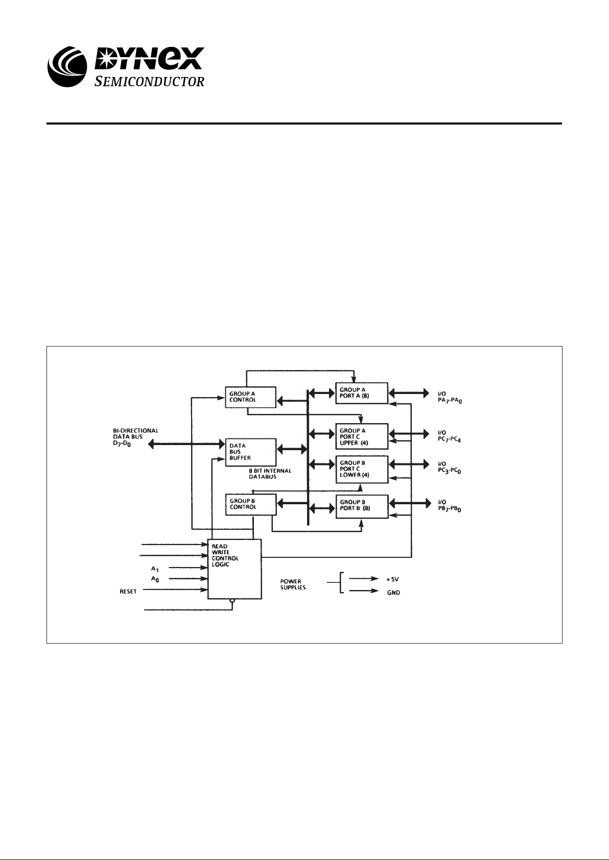
Figure 1: Block Diagram
RD/WN
DSN
CSN
MA28155
Radiation Hard Programmable
Peripheral Interface
Replaces June 1999 version, DS3575-4.0 DS3575-5.0 January 2000
Page 2

MA28155
2/20
FUNCTIONAL DESCRIPTION
The MA28155 is a programmable peripheral interface
(PPI) device designed for use with MAS281. Its function is that
of a general purpose l/O component to interface peripheral
equipment to the microcomputer system bus. The functional
configuration of the MA28155 is programmed by the system
software so that, normally, no external logic is necessary to
interface peripheral devices or structures.
Data Bus Buffer
This 3-state, bidirectional, 8-bit buffer is used to interface
the MA28155 to the system data bus. Data is transmitted or
received by the buffer upon execution of input or output
instructions by the CPU. Control words and status information
are also transferred through the data bus buffer.
Read/Write and Control Logic
The function of this block is to manage all of the internal
and external transfers of both Data and Control Status words.
It accepts inputs from the CPU Address and Control busses
and in turn, issues commands to both of the Control Groups.
Reset (RESET)
A high on this input clears the control register and all ports
(A,B,C) are set to the input mode.
Chip Select (CSN)
A low on this input pin enables the communication between
the MA28155 and the CPU.
Read/Write Select (RD/WN)
A high on RD/WN indicates a CPU read from the MA28155
and a low indicates a CPU data or control word write to the
MA28155. The RD/WN line is active only when DSN is low.
Data Strobe (DSN)
This input indicates that a data transfer is taking place.
During a CPU write operation the MA28155 reads data from
the bus on the rising edge of DSN. During a read operation the
MA28155 outputs data to the bus while DSN is low. Data is
valid on the rising edge of DSN.
Port Select O and Port Select 1 (AO and A1 )
These input signals, in conjunction with the DSN and RD/
WN inputs, control the selection of one of the three ports of the
control word registers. They are normally connected to the
least significant bits of the address bus.
Basic Operation
A1
0
0
1
0
0
1
1
x
1
x
A0
0
1
0
0
1
0
1
x
1
x
RD/
WNWN
WNWN
WN
1
1
1
0
0
0
0
x
1
x
CSNCSN
CSNCSN
CSN
0
0
0
0
0
1
1
1
0
0
READ
PORT A → DATA BUS
PORT B → DATA BUS
PORT C → DATA BUS
WRITE
DATA BUS → PORT A
DATA BUS → PORT B
DATA BUS → PORT C
DATA BUS → CONTROL
DISABLE
DATA BUS → TRI-STATE
ILLEGAL CONDITION
DATA BUS → TRI-STATE
DSNDSN
DSNDSN
DSN
0
0
0
0
0
0
0
x
0
1
Table 1: Basic Operation
OPERATIONAL DESCRIPTION
Mode Selection
There are three basic modes of operation, which can be
selected by the system software:
Mode 0. Basic Input/Output
Mode 1. Strobed Input/Output
Mode 2 Bi-directional Bus
When the reset input goes high all ports will be set to the
input mode (i.e. all 24 lines will be in the high impedance state)
After the reset is removed the MA28155 can remain in the
input mode with no additional initialisation required.
During the execution of the system program any of the
other modes may be selected using a single output instruction.
This allows a single MA28155 to service a variety of peripheral
devices with a single software maintenance routine.
The modes for Port A and Port B can be separately
defined, while Port C is divided into two portions as required by
the Port A and Port B definitions. All of the output registers,
including the status register, will be reset whenever the mode
is changed.
Modes may be combined so that their functional definition
can be tailored to almost any l/O structure. For instance; Group
B can be programmed in Mode 0 whilst Group A could be
simultaneously programmed in Mode 1.
Page 3
MA28155
3/20
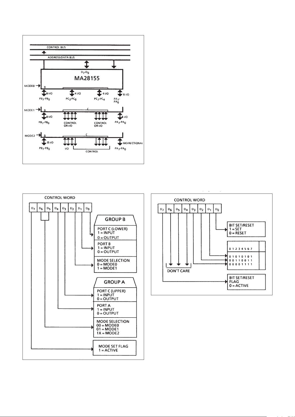
Figure 2: Basic Mode Definitions and Bus Interface
Mode Definition Format (D7= 1)
Single Bit Set/Reset Feature
Any of the eight bits of Port C can be Set or Reset using a
single output instruction. This feature reduces software
requirements in control-based applications.
When Port C is being used as Status/Control for Port A or
B, these bits can be set or reset by using the Bit Set/Reset
operation just as if they were data output ports.
Interrupt Control Functions
When the MA28155 is programmed to operate in Mode 1
or 2, control signals are provided that can be used as interrupt
request inputs to the CPU (figure 4). The interrupt request
signals, generated from Port C, can be inhibited or enabled by
setting or resetting the associated INTE register bit, using the
Bit Set/Reset function of Port C.
This function allows the programmer to disallow or allow a
specific l/O device to interrupt the CPU, without affecting any
other device in the interrupt structure.
INTE register bit definitions:
(BIT-SET): INTE is SET -Interrupt enable
(BIT-RESET): INTE is RESET -Interrupt disable
Note: All mask register bits are automatically reset during
mode selection and device reset.
Bit Set/Reset Format (D7 = 0)
Figure 4: Bit Set/Reset Format (D7 = 0)
Figure 3: Mode Definition Format (D7 = 1)
RD/WN, DSN
A0 - A1, CSN
BIT No.
S
E
L
B
0
B
1
B
2
A
A
A
C
Page 4
MA28155
4/20
OPERATING MODE 0
(Basic Input/Output)
This functional configuration provides simple input and
output operation for each of the three ports. No handshaking is
required; data is simply written to or read from a specified port.
■ Two 8-bit ports and 4-bit ports
■ Any port can be input or output
■ Outputs are latched
■ Inputs are not latched.
■ 16 different Input/Output configurations are possible in this
Mode.
Group A and Group B Controls
The functional configuration of each port is programmed by
the system software. In essence, the CPU outputs a control
word to the MA28155. The control word contains information
such as mode, bit set, bit reset, etc., this initializes the
functional configuration of the MA28155.
Each of the Control blocks (Group A and Group B) accept
commands from the Read/Write Control Logic, receive control
words from the internal data bus and issue the proper
commands to its associated ports:
Control Group A - Port A and Port C upper (C7-C4) Control
Group B - Port B and Port C lower (C3-C0)
The Control Word Register can only be written into.
Therefore reading of the Control Word Register is not allowed .
Ports A, B and C
The MA28155 contains three 8-bit ports (A, B, and C). All
can be configured in a wide variety of functional characteristics
by the system software but each has its own special features
to further enhance the power and flexibility of the MA28155.
Port A.
One 8-bit data output latch/buffer and one 8-bit data input
latch.
Port B.
One 8-bit data input/output latch/buffer and one 8-bit input
buffer
Port C.
One 8-bit data output latch/buffer and one 8-bit data input
buffer (no latch for input) This port can be divided into two 4-bit
ports under the mode control. Each 4-bit port contains a 4-bit
latch and it can be used for the control signal outputs and
status signal inputs in conjunction with ports A and B
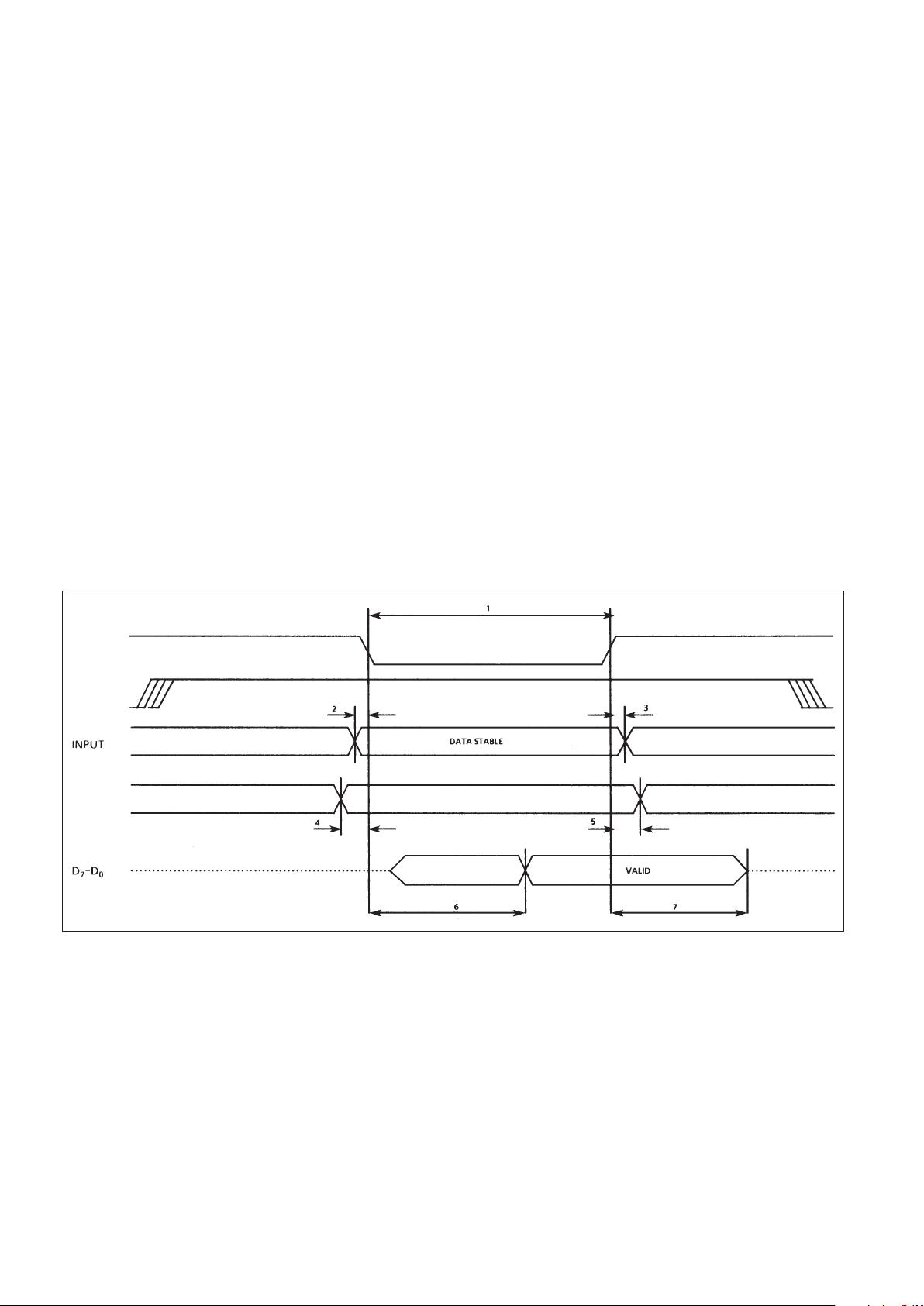
Figure 5: Basic Input (Read) Timing Diagram
DSN
CSN, A1, A0
RD/WN
RD/WN set-up and hold time
Page 5
MA28155
5/20
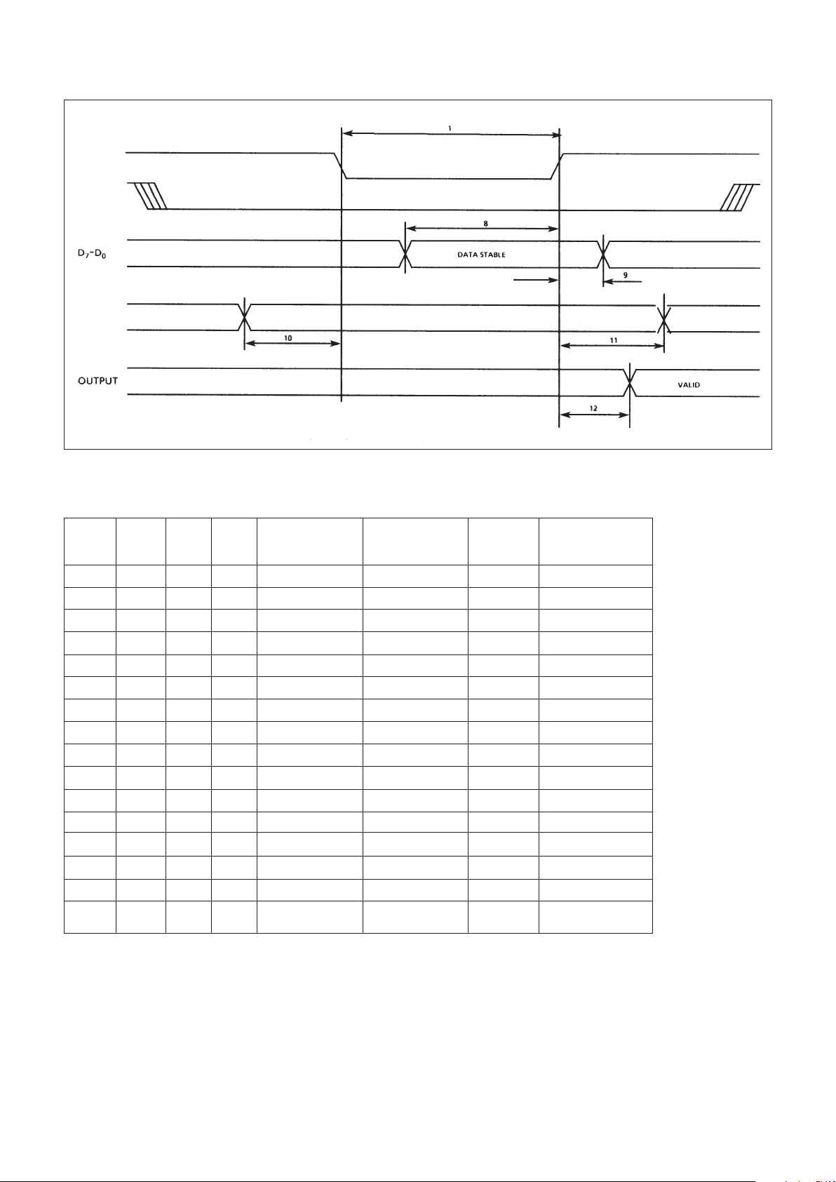
Figure 6: Basic Input (Write) Timing Diagram
D
4
D
3
D
1
D
0
PORT A PORT C PORT B PORT C
(UPPER) (LOWER)
0 0 0 0 OUTPUT OUTPUT OUTPUT OUTPUT
0 0 0 1 OUTPUT OUTPUT OUTPUT INPUT
0 0 1 0 OUTPUT OUTPUT INPUT OUTPUT
0 0 1 1 OUTPUT OUTPUT INPUT INPUT
0 1 0 0 OUTPUT INPUT OUTPUT OUTPUT
0 1 0 1 OUTPUT INPUT OUTPUT INPUT
0 1 1 0 OUTPUT INPUT INPUT OUTPUT
0 1 1 1 OUTPUT INPUT INPUT INPUT
1 0 0 0 INPUT OUTPUT OUTPUT OUTPUT
1 0 0 1 INPUT OUTPUT OUTPUT INPUT
1 0 1 0 INPUT OUTPUT INPUT OUTPUT
1 0 1 1 INPUT OUTPUT INPUT INPUT
1 1 0 0 INPUT INPUT OUTPUT OUTPUT
1 1 0 1 INPUT INPUT OUTPUT INPUT
1 1 1 0 INPUT INPUT INPUT OUTPUT
1 1 1 1 INPUT INPUT INPUT INPUT
Table 2: Port Definition Mode 0 (See Also Figure 3)
Port Definition Mode 0
RD/WN set-up and hold time
DSN
RD/WN
CSN, A1, A0
Page 6
MA28155
6/20
OPERATING MODE 1
(Strobed Input/Output)
This functional configuration provides a means for
transferring l/O data to or from a specified port in conjunction
with strobes or handshaking signals. In mode 1, port A and
port B use the lines on port C to generate or accept these
handshaking signals
■ Two Groups (Group A and Group B) .
■ Each Group contains one 8-bit data port and one 4-bit
control/data port,
■ The 8-bit data port can be either input or output, Both
inputs and outputs are latched,
■ The 4-bit port is used for control and status of the 8-bit data
port.
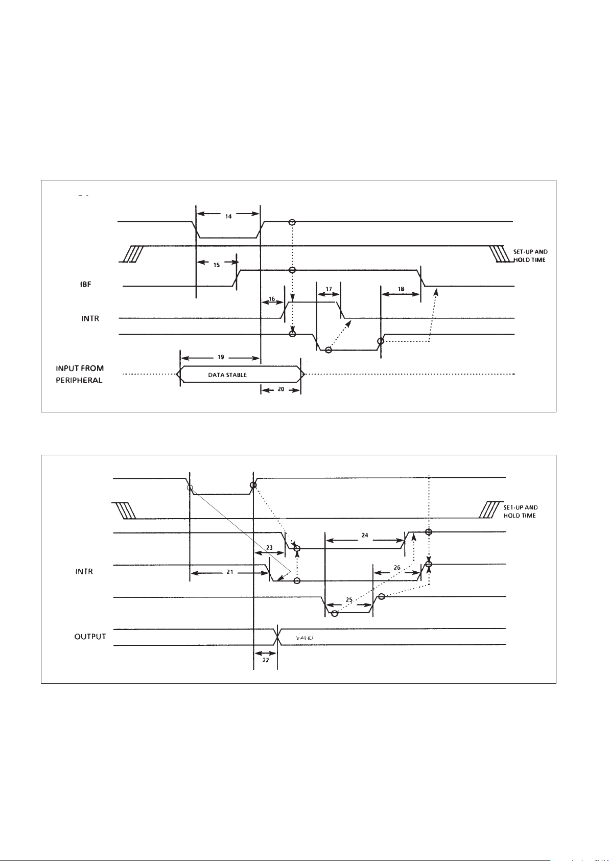
Figure 7: Strobed Input Timing Diagram
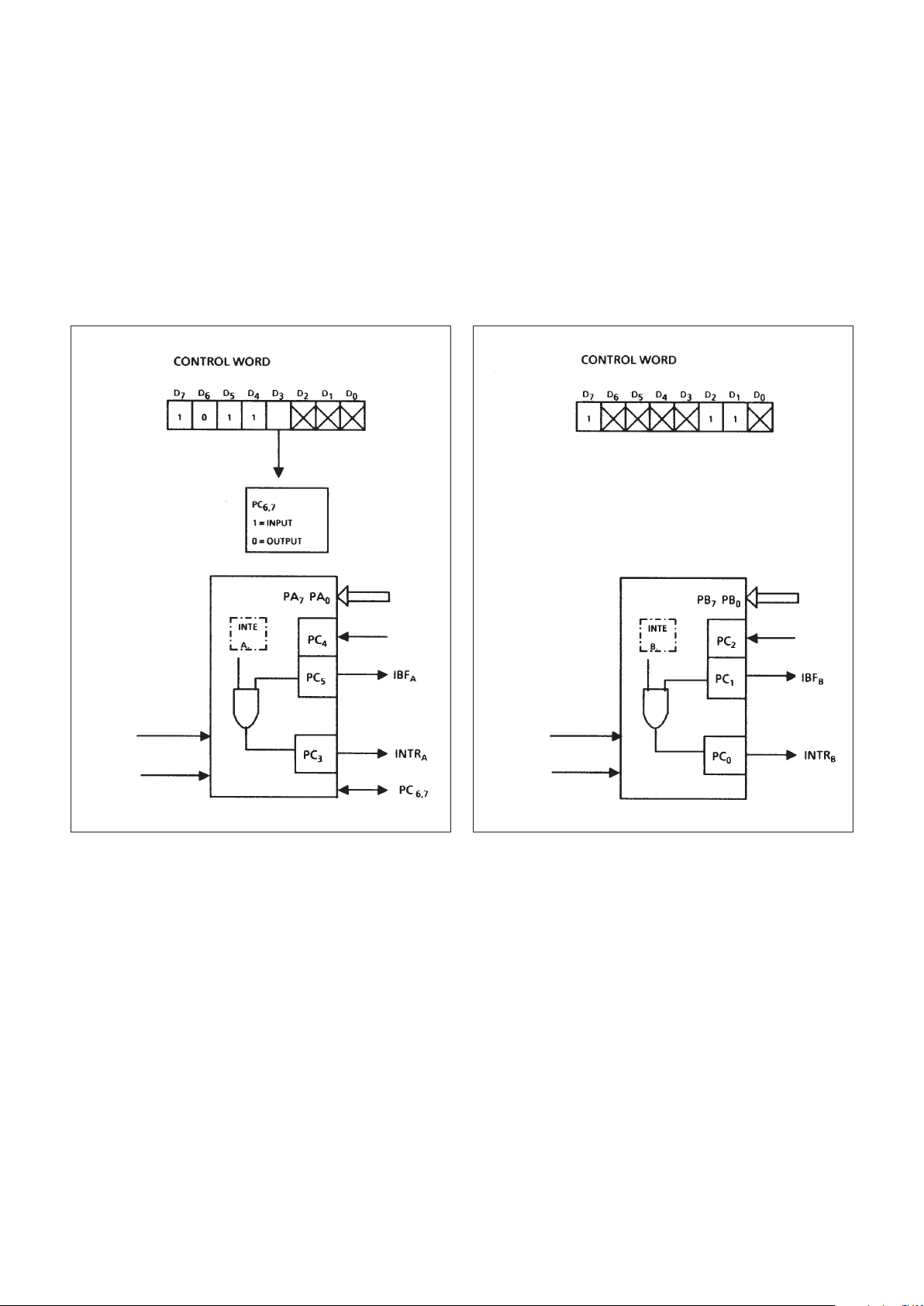
Figure 8: Strobed Output Timing Diagram
DSN
RD/WN
STBN
OBFN
RD/WN
DSN
ACKN
Page 7
MA28155
7/20
Input Control Signal Definition (Mode 1)
STBN (Strobe Input).
A low on this input loads data into the input latch.
IBF (Input Buffer Full Register Bit).
A high on this output indicates that the data has been
loaded into the input latch; in essence, an acknowledgement.
IBF is set by a STBN active pulse (which strobes data into
the device), and is reset by the rising edge of DSN (which
reads the latched data out of the device).
INTR (Interrupt Request).
A high on this output can be used to interrupt the CPU
when an input device is requesting service, INTR is set by the
STBN being high and IBF being high and INTE being enabled,
It is reset by the falling edge of DSN, This procedure allows an
input device to request service from the CPU by simply
strobing its data into the port,
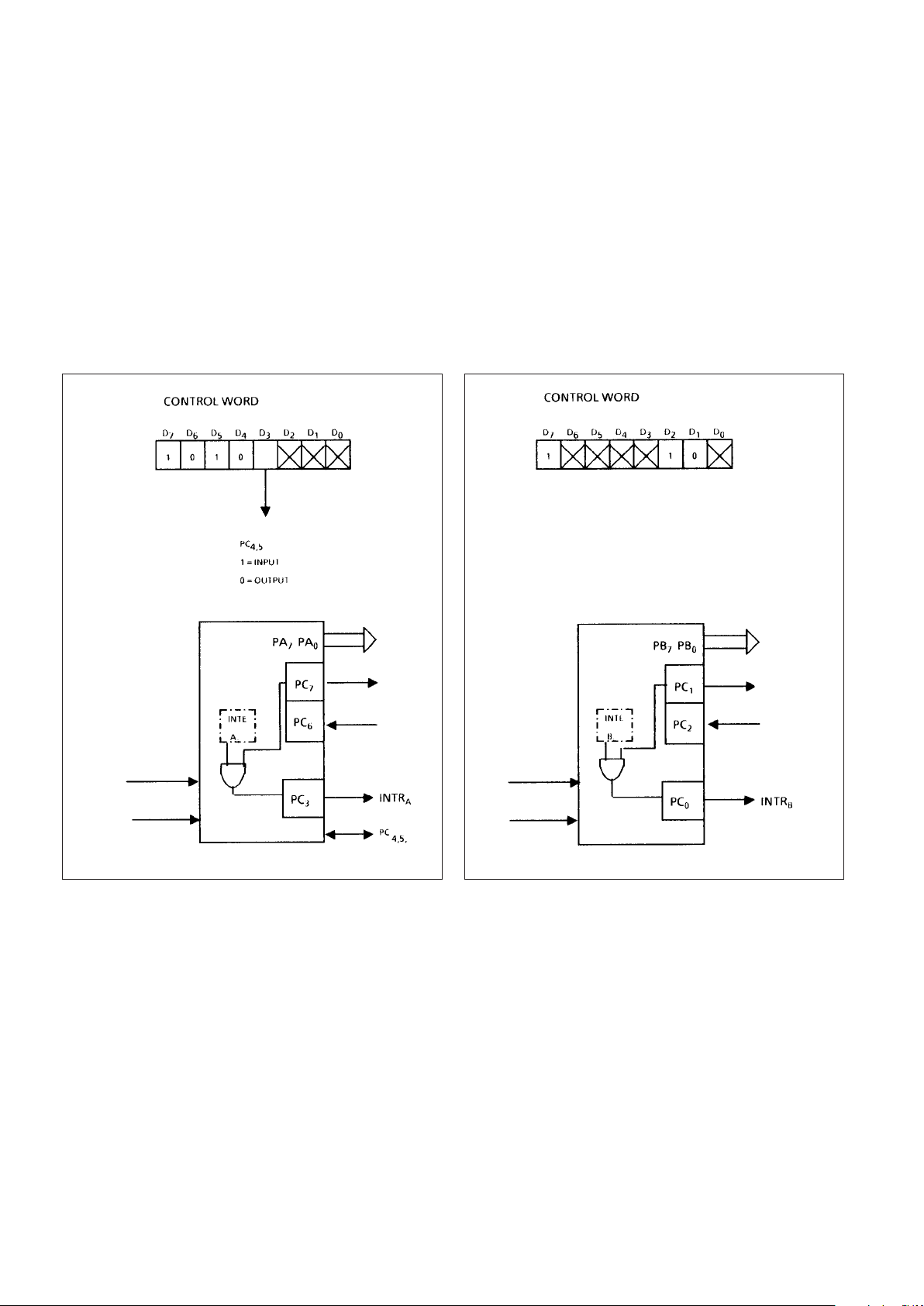
INTE A: Controlled by bit set/reset of PC
4
INTE B: Controlled by bit set/reset of PC
2
Figure 9: Strobed Input (PORT A) Figure 10: Strobed Input (PORT B)
DSN
DSN
RD/WN
RD/WN
STB
A
N
STB
B
N
Page 8
MA28155
8/20
Output Control Signal Definition (Mode 1)
OBFNOBFN
OBFNOBFN
OBFN (Output Buffer Full Register Bit).
The OBFN output will go low to indicate that the CPU has
written data out to the specified port. The OBF register bit will
be set by the rising edge of the DSN input and reset by ACKN
input being low.
ACKN ACKN
ACKN ACKN
ACKN (Acknowledge Input).
A low on this input informs the 28155 that the data from
port A or port B has been accepted; in essence, a response
from the peripheral device indicating that it has received the
data output by the CPU.
INTR (Interrupt Request).
A high on this output can be used to interrupt the CPU
when an output device has accepted data transmitted by the
CPU. INTR is set when ACKN is high, OBFN is high and INTE
is high. It is reset by the falling edge of DSN.
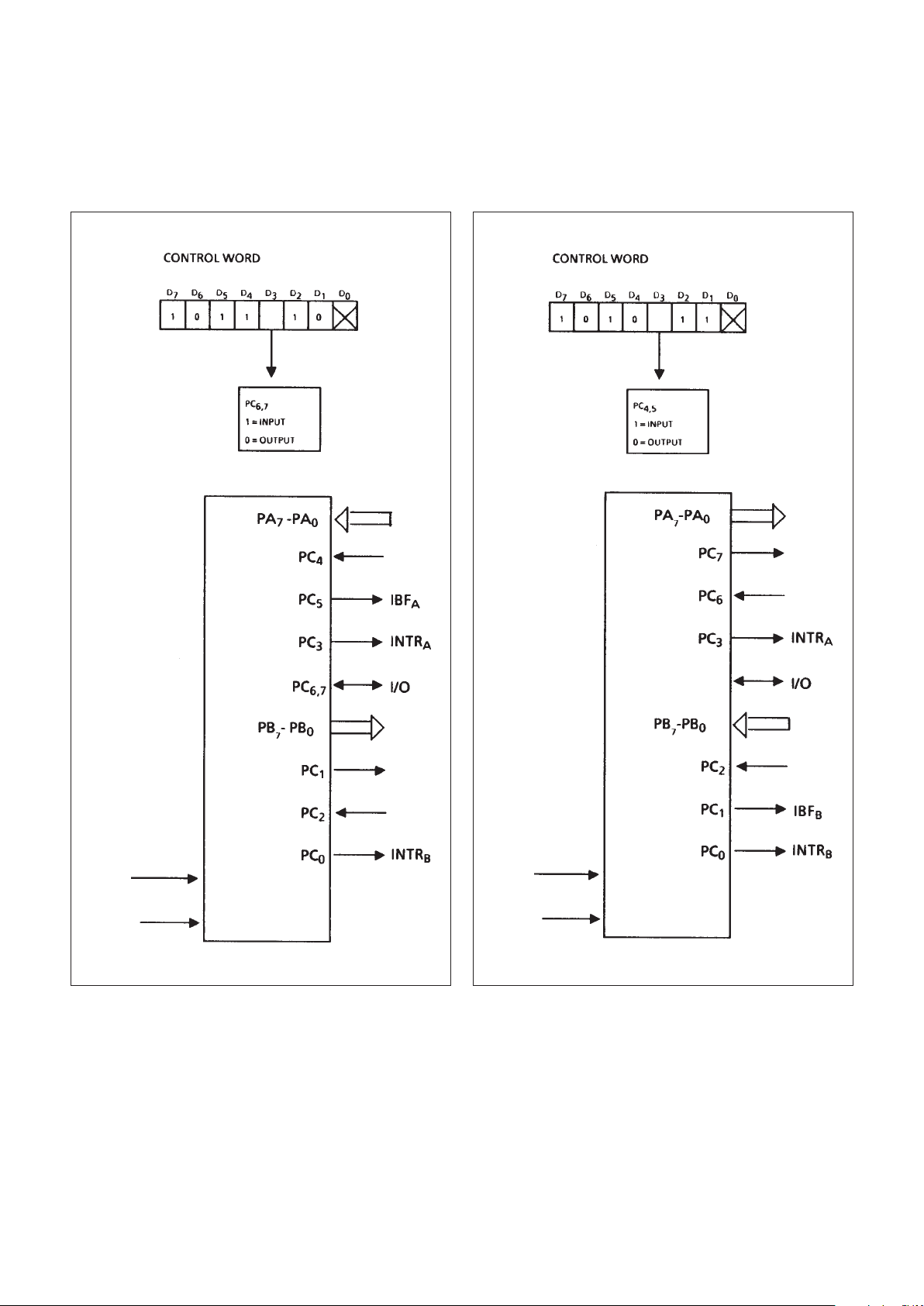
INTE A: Controlled by bit set/reset of PC
6
INTE B: Controlled by bit set/reset of PC
2
Figure 11: Strobed Output (PORT A) Figure 12: Strobed Output (PORT B)
DSN
RD/WN
ACK
A
N
OBF
A
N
RD/WN
DSN
ACK
B
N
OBF
B
N
Page 9
MA28155
9/20
Combinations of Mode 1
Port A and Port B can be individually defined as input or
output in Mode 1 to support a wide variety of strobed l/O
applications.
Figure 13: PORT A (STROBED INPUT)
PORT B (STROBED OUTPUT)
Figure 14: PORT A (STROBED OUTPUT)
PORT B (STROBED INPUT)
DSN
RD/WN
STB
A
N
OBFBN
ACK
B
N
DSN
RD/WN
STBBN
OBF
A
N
ACK
A
N
PC
4,5
Page 10
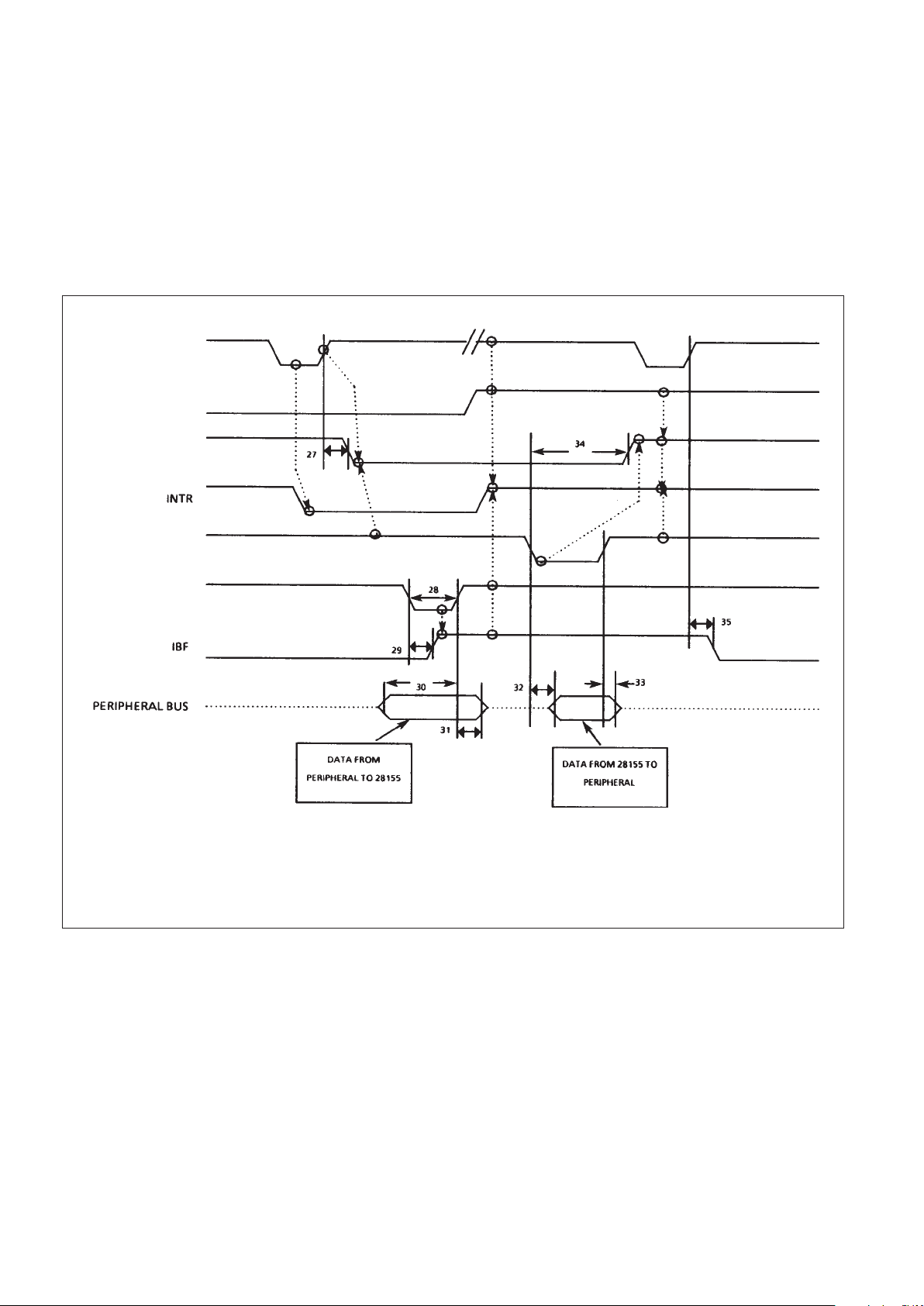
MA28155
10/20
OPERATING MODE 2
(Strobed Bidirectional Bus I/0)
This functional configuration provides a means for
communicating with a peripheral device or structure on a
single 8-bit bus for both transmitting and receiving data
(bidirectional bus l/O) . Handshaking signals are provided to
maintain proper bus flow discipline in a similar manner to Mode
1, Interrupt generation and enable/disable functions are also
available.
■ Used in group A only.
■ One 8-bit bidirectional bus port (port A) and 5-bit control
port (port C).
■ Both inputs and outputs are latched,
■ The 5-bit control port (port C) is used for control and status
of the 8-bit bidirectional bus port (port A).
NOTE:
Any sequence where RD/WN = 0 coincident with DSN low occurs before ACKN and STBN occurs before RD/WN = 1
coincident with DSN is permissable
(INTR = IBF MASK STBN (RD/WN = 1. DSN = 0) + OBFN MASK ACKN (RD/WN = 0. DSN = 0))
Figure 15: Bidirectional Timing Diagram
DSN
RD/WN
OBFN
ACKN
STBN
Page 11
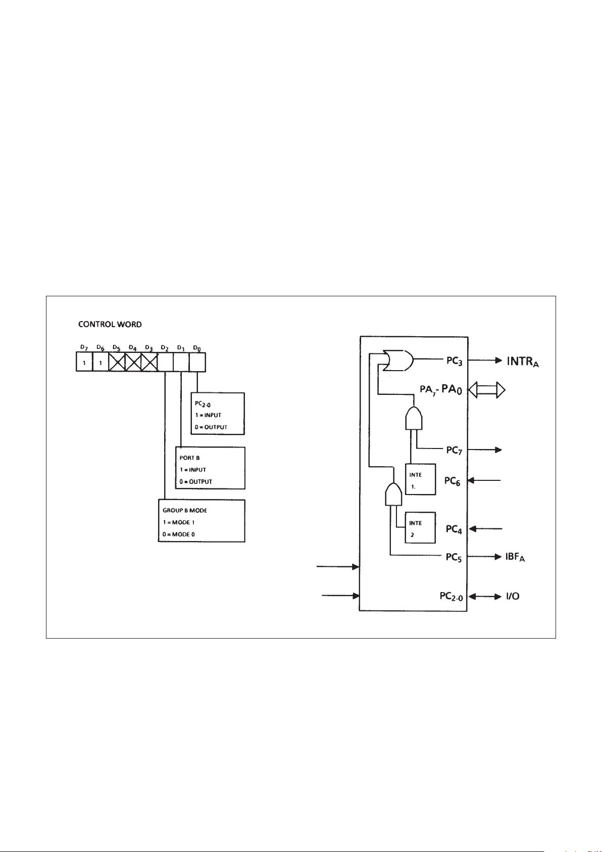
MA28155
11/20
BIDIRECTIONAL BUS L/O CONTROL
Signal Definition (Mode 2)
INTR (Interrupt Request):
A high on this output can be used to interrupt the CPU for
both input or output operations.
Output Operations
OBFN (Output Buffer Full):
The OBF output will go low to indicate that the CPU has
written data out to port A.
ACKN (Acknowledge):
A low on this input enables the tri-state output buffer of port
A to send out the data. Otherwise, the output buffer will be in
the high impedance state,
INTE 1 (INTE register bit associated with OBFN):
Controlled by Bit Set/Reset of PC
6
.
Input Operations
STBN (Strobe input):
A low on this input loads data in to the input latch,
IBF (Input Buffer Full Register Bit):
A high on this output indicates data has been loaded in to
the input latch,
INTE 2 (The INTE register bit associated with IBF).
Controlled by Bit Set/Reset of PC
4
.
Figure 16: Mode 2 Bidirectional
DSN
RD/WN
OBF
A
N
ACK
A
N
STBAN
Page 12
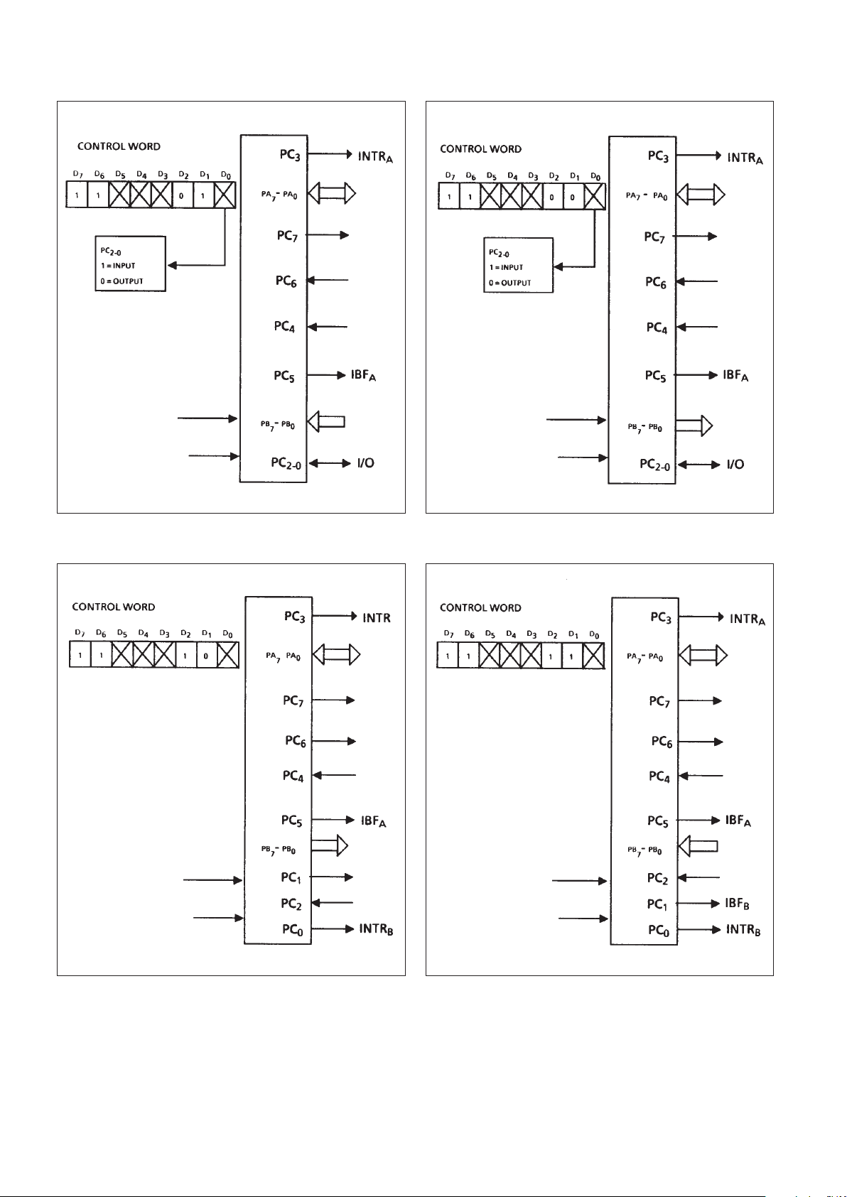
MA28155
12/20
Figure 17a: Mode 2 and Mode 0 (Input) Figure 17b: Mode 2 and Mode 0 (Output)
Figure 17c: Mode 2 and Mode 1 (Output) Figure 17d: Mode 2 and Mode 1 (Input)
OBFAN
ACKAN
STB
A
N
DSN
RD/WN
DSN
RD/WN
OBFAN
ACK
A
N
STBAN
OBFAN
ACKAN
STB
A
N
DSN
RD/WN
ACKBN
OBF
B
N
DSN
RD/WN
OBFAN
ACKAN
STB
A
N
STBBN
A
Page 13

MA28155
13/20
Mode Definition Summary
MODE 0 MODE 1 MODE 2
IN OUT IN OUT
PA
0
IN OUT IN OUT ⇐ ⇒
PA
1
IN OUT IN OUT ⇐ ⇒
PA
2
IN OUT IN OUT ⇐ ⇒
PA
3
IN OUT IN OUT ⇐ ⇒
PA
4
IN OUT IN OUT ⇐ ⇒
PA
5
IN OUT IN OUT ⇐ ⇒
PA
6
IN OUT IN OUT ⇐ ⇒
PA
7
IN OUT IN OUT ⇐ ⇒
PB
0
IN OUT IN OUT PORT B MODE 0 or 1
PB
1
IN OUT IN OUT PORT B MODE 0 or 1
PB
2
IN OUT IN OUT PORT B MODE 0 or 1
PB
3
IN OUT IN OUT PORT B MODE 0 or 1
PB
4
IN OUT IN OUT PORT B MODE 0 or 1
PB
5
IN OUT IN OUT PORT B MODE 0 or 1
PB
6
IN OUT IN OUT PORT B MODE 0 or 1
PB
7
IN OUT IN OUT PORT B MODE 0 or 1
PC
0
IN OUT INTR
B
INTR
B
I/O
PC
1
IN OUT IBF
B
OBF
B
N I/O
PC
2
IN OUT STBBN ACKBN I/O
PC
3
IN OUT INTR
A
INTR
A
INTR
A
PC
4
IN OUT STBAN I/O STBAN
PC
5
IN OUT IBF
A
I/O IBF
A
PC
6
IN OUT I/O ACKAN ACKAN
PC
7
IN OUT I/O OBFAN OBFAN
Table 3: Mode Definition Summary
Page 14
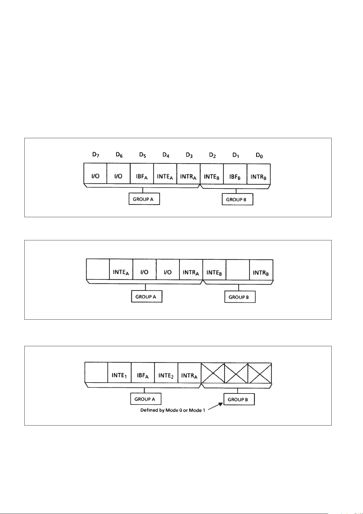
MA28155
14/20
Reading Port C Status.
In Mode 0 Port C transfers data from or to the peripheral
device, When the MA28155 is programmed to function in
Modes 1 or 2 Port C generates or accepts handshaking signals
with the peripheral device, Reading the contents of Port C
allows the programmer to test or verify the status of each
peripheral device and change the program flow accordingly.
There is no special instruction to read the Status
Information from Port C. A normal read operation of Port C is
executed to perform this function.
Special Mode Combination Considerations.
There are several combinations of modes when not all of
the bits in port C are used for control or status. The remaining
bits can be used as follows:
If programmmed as inputs-
All input lines can be accessed during normal port C
read.
If programmed as outputs
Bits in C upper (PC7-PC4) must be individually
accessed using a bit set/reset function.
Bits in C lower (PC3-PC0) can be accessed using the bit
set/reset function or bits PC2-PC0 may also be accessed as a
trio by writing into port C.
Figure 18b: Mode 1 Output Configuration
Figure 18c: Mode 2
Figure 18a: Mode 1 Input Configuration
OBFAN
OBF
B
N
OBF
A
N
Page 15

MA28155
15/20
DEFINITION OF SUBGROUPS
Subgroup Definition
1 Static characteristics specified in Table 5 at +25°C
2 Static characteristics specified in Table 5 at +125°C
3 Static characteristics specified in Table 5 at -55°C
7 Functional characteristics specified at +25°C
8A Functional characteristics specified at +125°C
8B Functional characteristics specified at -55°C
9 Switching characteristics specified in Table 6 at +25°C
10 Switching characteristics specified in Table 6 at +125°C
11 Switching characteristics specified in Table 6 at -55°C
DC CHARACTERISTICS AND RATINGS
Parameter Min Max Units
Supply Voltage -0.5 7 V
Input Voltage -0.3 VDD+0.3 V
Current Through Any Pin -20 +20 mA
Operating Temperature -55 125 °C
Storage Temperature -65 150 °C
Note: Stresses above those listed may cause permanent
damage to the device. This is a stress rating only and
functional operation of the device at these conditions, or at
any other condition above those indicated in the operations
section of this specification, is not implied. Exposure to
absolute maximum rating conditions for extended periods
may affect device reliability.
Table 4: Absolute Maximum Ratings
Total dose radiation not
exceeding 3x10⁵ Rad(SI)
Symbol Parameter Conditions Min Typ Max Units
V
DD
Supply Voltage - 4.5 5.0 5.5 V
V
IH
Input High Voltage - 2.2 - - V
V
IL
Input Low Voltage - - - 0.8 V
V
OH
Output High Voltage IOH = -6mA 3.5 - - V
V
OL
Output Low Voltage IOL = 12mA - - 0.5 V
I
IN
Input Leakage Current (Note 1) VDD = 5.5V, - - ±10 µA
VIN = V
SS
or V
DD
I
OZ
Tristate Leakage Current (Note 1) VDD = 5.5V, - - ±50 µA
V
IN
= V
SS
or V
DD
I
DD
Power Supply Current Static, - 0.1 10 mA
Note 1: Guaranteed but not tested at -55°C
Mil-Std-883, method 5005, subgroups 1, 2, 3.
VDD = 5V±10%, over full operating temperature range.
Table 5: Electrical Characteristics
Page 16

MA28155
16/20
AC ELECTRICAL CHARACTERISTICS
Parameter Min. Max. Units Parameter Min. Max Units
18 DSN ⇑ to lBF ⇑ -65ns
19 Peripheral Data set up to STBN ⇑ 0ns
1DSN width 65 - ns 20 Peripheral Data hold after STBN ⇑ 100 ns
2 Peripheral Data set up to DSN 0 - ns 21 DSN ⇓ to INTR ⇓ (note 4) - DS+ ns
100
3 Peripheral Data hold after DSN 10 - ns 22 Output valid from DSN ⇑ - 100 ns
4 CSN, A1, A0 setup to DSN ⇓ 0 - ns 23 DSN ⇑ to OBFN ⇓ - 105 ns
5 CSN, A1, A0 hold after DSN ⇑ 0 - ns 24 ACKN ⇑ to OBFN ⇓ -50ns
6 Data valid from DSN ⇓ -60ns25ACKN pulse width 100 - ns
7 Data float from DSN ⇑ (note 5) 10 100 ns 26 ACKN ⇑ INTR ⇑ -80ns
8 Data set up to DSN ⇓ 20 - ns 27 DSN ⇑ to OBFN ⇓ - 105 ns
9 Data hold after DSN ⇑ 30 - ns 28 STBN pulse width 100 - ns
10 CSN, A1, A0 setup to DSN ⇓ 0 - ns 29 STBN ⇓ to IBF ⇑ -65ns
11 CSN, A1, A0 hold after DSN ⇑ 20 - ns 30 Peripheral Data set up to STBN ⇑ 0-ns
12 Output valid from DSN ⇑ - 100 ns 31 Perlpheral Data hold after STBN ⇑ 100 - ns
14 STBN pulse width 100 - ns 32 Output valid from ACKN ⇓ -45ns
15 STBN ⇓ to IBF ⇑ - 65 ns 33 Output float from ACKN ⇑ (Note 5) 10 100 ns
16 STBN ⇑ to INTR ⇑ -65ns34ACKN ⇓ to OBFN ⇑ -50ns
17 DSN ⇓, to INTR ⇓ -65ns35DSN ⇑ to IBF ⇓ -65ns
Mil-Std-883, method 5005, subgroup 9, 10, 11.
1. VDD = 5V±10% and CCL = 50pF, over full operating temperature range.
2. Input Pulse VSS to 3.0 Volts.
3. Times Measurement Reference Level 1.5 Volts.
4. DSN = Data Strobe Pulse Width.
5. Measured by a 1.0 Volt change in output voltage. Outputs tied to VSS via 680Ω.
Table 6: AC Electrical Characteristics
Page 17
MA28155
17/20
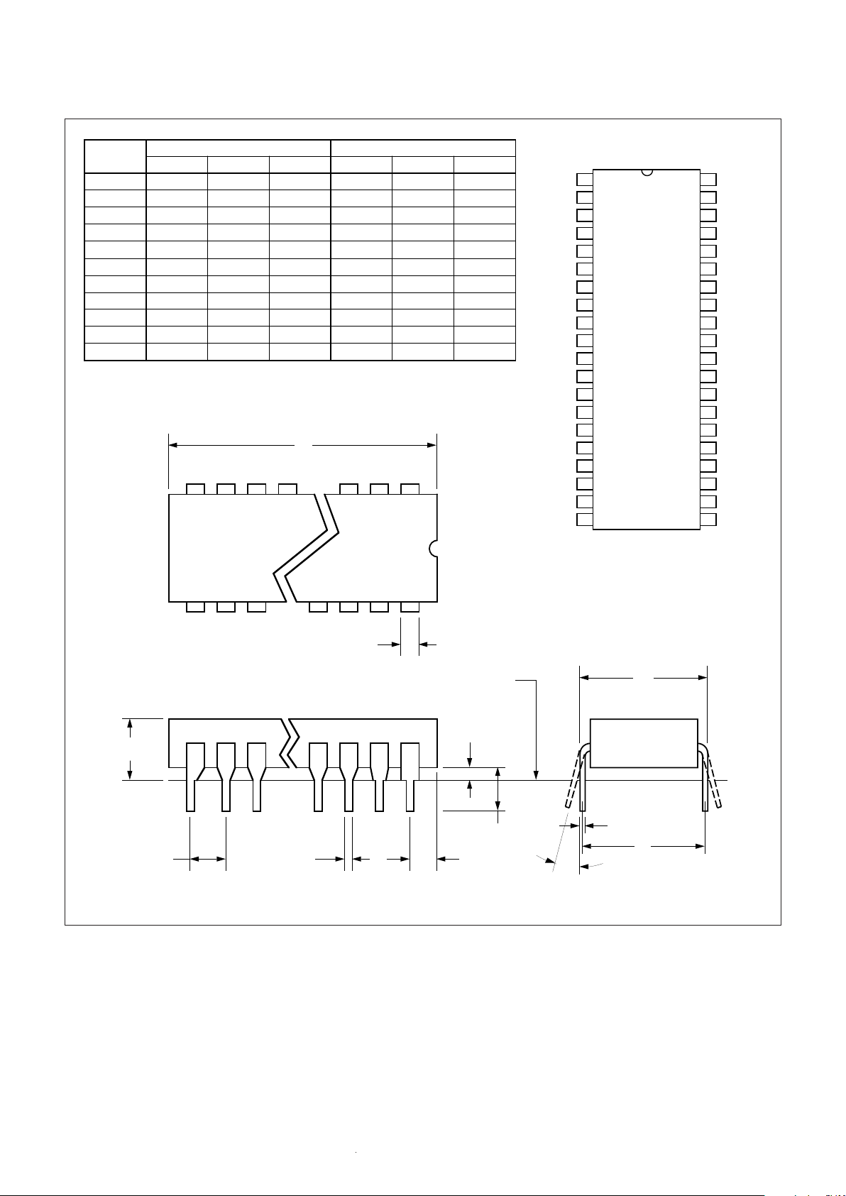
PACKAGE OUTLINES & PIN ASSIGNMENTS
Ref
Millimetres Inches
Min. Nom. Max. Min. Nom. Max.
A - - 5.715 - - 0.225
A1 0.38 - 1.53 0.015 - 0.060
b 0.35 - 0.59 0.014 - 0.023
c 0.20 - 0.36 0.008 - 0.014
D - - 51.31 - - 2.020
e - 2.54 Typ. - - 0.100 Typ. -
e1 - 15.24 Typ. - - 0.600 Typ. -
H 4.71 - 5.38 0.185 - 0.212
Me - - 15.90 - - 0.626
Z - - 1.27 - - 0.050
W - - 1.53 - - 0.060
XG405
D
W
A
e b Z
H
A
1
15°
M
E
C
e
1
Seating Plane
120
4021
Figure 19: 40-Lead Ceramic DIL (Solder Seal) - Package Style C
1
PA3
2
PA2
3
PA1
4
PA0
5
DSN
6
CSN
7
Vss
8
A1
9
A0
10
PC
7
Top
View
11
PC6
12
PC5
13
PC
4
14PC0
15
PC1
16
PC2
17
PC
3
18PB0
19
PB1
20
PB2
40
PA4
39
PA5
38
PA6
37
PA7
36
RD/WN
35
RESET
34
D0
33
D1
32
D2
31
D3
30
D4
29
D5
28
D6
27
D7
26
Vdd
25
PB7
24
PB6
23
PB5
22
PB4
21
PB3
Page 18
MA28155
18/20
Ref
Millimetres Inches
Min. Nom. Max. Min. Nom. Max.
A - - 2.41 - - 0.095
b1 - 0.64 - - 0.025 -
D 16.33 - 16.81 0.643 - 0.662
E 16.33 - 16.81 0.643 - 0.662
e - 1.27 - - 0.050 Z - 1.91 Typ. - - 0.075 Typ. -
XG446
Bottom
View
Pad 1
Radius r
3 corners
E
Z
e b
1
D A
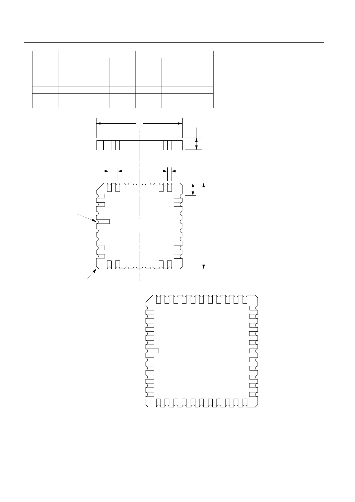
Figure 20: 44-Pad Leadless Chip Carrier (Package Style L)
Bottom
View
18
1716151413121110987
19
20
21
22
23
24
25
26
27
28
2930313233343536373839
6
543
2
1
44
43
42
41
40
PC2
PC3
PB0
PB1
PB2
PB3
PB4
PB5
PB6
PB7
N
CNCDS
N
PA0
PA1
PA2
PA3
PA4
PA5
PA6
PA7
RD
/
WN
CS
N
Vss
A1
A0
PC7
PC6
PC5
PC4
PC0
PC1
NC
NC
RESET
D0
D1
D2
D3
D4
D5
D6
D7
Vdd
Page 19
MA28155
19/20
RADIATION TOLERANCE
Total Dose Radiation Testing
For product procured to guaranteed total dose radiation
levels, each wafer lot will be approved when all sample
devices from each lot pass the total dose radiation test.
The sample devices will be subjected to the total dose
radiation level (Cobalt-60 Source), defined by the ordering
code, and must continue to meet the electrical parameters
specified in the data sheet. Electrical tests, pre and post
irradiation, will be read and recorded.
Dynex Semiconductor can provide radiation testing
compliant with Mil-Std-883 test method 1019, Ionizing
Radiation (Total Dose).
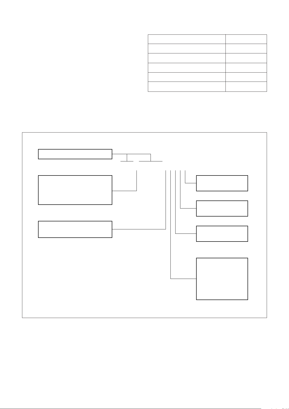
ORDERING INFORMATION
For details of reliability, QA/QC, test and assembly
options, see ‘Manufacturing Capability and Quality
Assurance Standards’ Section 9.
Unique Circuit Designator
S
R
Q
H
Radiation Hard Processing
100 kRads (Si) Guaranteed
300 kRads (Si) Guaranteed
1000 kRads (Si) Guaranteed
Radiation Tolerance
CLCeramic DIL (Solder Seal)
Leadless Chip Carrier
Package Type
QA/QCI Process
(See Section 9 Part 4)
Test Process
(See Section 9 Part 3)
Assembly Process
(See Section 9 Part 2)
L
C
D
E
B
S
Rel 0
Rel 1
Rel 2
Rel 3/4/5/STACK
Class B
Class S
Reliability Level
MAx28155xxxxx
Total Dose (Function to specification)* 3x10⁵ Rad(Si)
Transient Upset (Stored data loss) 5x10¹⁰ Rad(Si)/sec
Transient Upset (Survivability) >1x10
12
Rad(Si)/sec
Neutron Hardness (Function to specification) >1x10¹⁵ n/cm
2
Single Event Upset** <1x10
-10
Errors/bit day
Latch Up Not possible
* Other total dose radiation levels available on request
** Worst case galactic cosmic ray upset - interplanetary/high altitude orbit
Figure 21: Radiation Hardness Parameters
Page 20

MA28155
20/20
CUSTOMER SERVICE CENTRES
France, Benelux, Italy and Spain Tel: +33 (0)1 69 18 90 00. Fax: +33 (0)1 64 46 54 50
North America Tel: 011-800-5554-5554. Fax: 011-800-5444-5444
UK, Germany, Scandinavia & Rest Of World Tel: +44 (0)1522 500500. Fax: +44 (0)1522 500020
SALES OFFICES
France, Benelux, Italy and Spain Tel: +33 (0)1 69 18 90 00. Fax: +33 (0)1 64 46 54 50
Germany Tel: 07351 827723
North America Tel: (613) 723-7035. Fax: (613) 723-1518. Toll Free: 1.888.33.DYNEX (39639) /
Tel: (831) 440-1988. Fax: (831) 440-1989 / Tel: (949) 733-3005. Fax: (949) 733-2986.
UK, Germany, Scandinavia & Rest Of World Tel: +44 (0)1522 500500. Fax: +44 (0)1522 500020
These offices are supported by Representatives and Distributors in many countries world-wide.
© Dynex Semiconductor 2000 Publication No. DS3575-5 Issue No. 5.0 January 2000
TECHNICAL DOCUMENTATION – NOT FOR RESALE. PRINTED IN UNITED KINGDOM
HEADQUARTERS OPERATIONS
DYNEX SEMICONDUCTOR LTD
Doddington Road, Lincoln.
Lincolnshire. LN6 3LF. United Kingdom.
Tel: 00-44-(0)1522-500500
Fax: 00-44-(0)1522-500550
DYNEX POWER INC.
Unit 7 - 58 Antares Drive,
Nepean, Ontario, Canada K2E 7W6.
Tel: 613.723.7035
Fax: 613.723.1518
Toll Free: 1.888.33.DYNEX (39639)
This publication is issued to provide information only which (unless agreed by the Company in writing) may not be used, applied or reproduced for any purpose nor form part of any order or contract nor to be regarded
as a representation relating to the products or services concerned. No warranty or guarantee express or implied is made regarding the capability, performance or suitability of any product or service. The Company
reserves the right to alter without prior notice the specification, design or price of any product or service. Information concerning possible methods of use is provided as a guide only and does not constitute any
guarantee that such methods of use will be satisfactory in a specific piece of equipment. It is the user's responsibility to fully determine the performance and suitability of any equipment using such information and
to ensure that any publication or data used is up to date and has not been superseded. These products are not suitable for use in any medical products whose failure to perform may result in significant injury
or death to the user. All products and materials are sold and services provided subject to the Company's conditions of sale, which are available on request.
All brand names and product names used in this publication are trademarks, registered trademarks or trade names of their respective owners.
http://www.dynexsemi.com
e-mail: [email protected]
Datasheet Annotations:
Dynex Semiconductor annotate datasheets in the top right hard corner of the front page, to indicate product status. The annotations are as follows:-
Target Information: This is the most tentative form of information and represents a very preliminary specification. No actual design work on the product has been started.
Preliminary Information: The product is in design and development. The datasheet represents the product as it is understood but details may change.
Advance Information: The product design is complete and final characterisation for volume production is well in hand.
No Annotation: The product parameters are fixed and the product is available to datasheet specification.
 Loading...