

Page 1
MA28140
1/72
The MA28140 Packet Telecommand Decoder (PTD) is a
single-chip implementation of the core part of a telecommand
decoder, manufactured using CMOS-SOS high performance,
radiation hard, 1.5µm technology. The PTD is a full
implementation of and fully compliant with the packet
telecommand standard ESA PSS-04-107 and the
telecommand decoder specification ESA PSS-04-151, these
being derived from the corresponding CCSDS standards.
The PTD, which handles 6 NRZ TC input channels,
processes the following layers:
Coding Layer
Transfer Layer
Segmentation Layer
Authentication Layer
Command Pulse Distribution
Some of these layers have a telemetry reporting
mechanism. The processed TC segment can be transferred to
the application either serially or in parallel.
CLCWSA
CLCWCA
CLCWDA
CLCWSB
CLCWCB
CLCWDB
CPDUS
FAR1S
FAR2S
AU1S
AU2S
TMC
TMD
PRDY
PBUS(0-15)
AUDIS
AUEXT
AUST
AUBUF
AUEND
AUR
AUTSL
AUSBUF
FARBUF
TCC0-5
TCS0-5
TCA0-5
VDD
GND
RFAVN
VCLSB
TMMOD
PAR
RESETN
CLK
PRIOR
TEST
MODE
CONF
SELTC(0-2)
DECOD
LADR(0-10)
LDAT(0-7)
RWN
BRQN
BGRN
RAMCSN
ROMCSN
LACCS
LACK
CPDUSTN
CPDUEN
CPDUDIV
MAPSTN
MAPCK
MAPDSR
MAPDTR
MAPDATA
MAPADT
PTD
14
12
1444442444443
123
144424443
123
123
Telemetry
Interface
Parallel
Interface
Authentication
Interface
Trans-
ponder
Interface
Power
144444244443
Miscellaneous
144424443
Local Bus
Interface
142443
MAP
Interface
123
CPDU
Interface
FEATURES
■ Single Chip Implementation of all TC Decoder Core
Functions
■ Built-in Authentication Unit
■ Built-in Command Pulse Distribution Unit Core Logic
■ Radiation Hard to 1MRads (Si)
■ High SEU Immunity, Latch-up Free
■ CMOS-SOS Technology
■ Conforms to CCSDS Standards
■ 6 NRZ TC Input Channels
■ 50Kbps Bit Rate
■ Low Power Consumption
■ Single 5V Supply
■ -55 to +125°C Operation
MA28140
Packet Telecommand Decoder
Replaces June 2000 version, DS3839-6.1 DS3839-7.0 September 2001
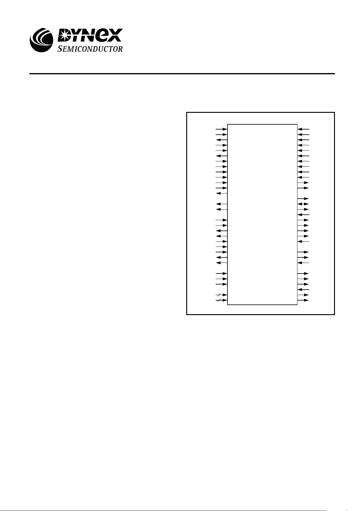
Pin connections
Page 2

MA28140
2/72
CONTENTS
Page
Front sheet ............................................................................1
1. Introduction .......................................................................2
2. TC Decoder Subsystem Overview ....................................3
3. PTD Architectural Overview ..............................................4
4. PTD Functional Description
4.1 Coding Layer .......................................................6
4.2 Transfer Layer .....................................................9
4.3 Authentication Layer ..........................................15
4.4 Segmentation Layer...........................................21
4.5 CPDU.................................................................22
4.6 Telemetry Reporting ..........................................24
5. PTD Interfaces
5.1 Physical Channel Interface ................................27
5.2 MAP Interface ....................................................27
5.3 Telemetry Interface............................................30
5.4 Parallel Interface................................................34
5.5 CPDU Interface..................................................35
5.6 Local Bus Interface ............................................36
5.7 Memories ...........................................................36
5.8 External Authentication......................................41
6. State After Reset.............................................................42
7. Signal Description ...........................................................44
8. Electrical Characteristics and Ratings
8.1 DC Parameters ..................................................47
8.2 AC Parameters ..................................................48
9. Package Details
9.1 Dimensions ........................................................65
9.2 Pin Assignment..................................................66
10. Radiation Tolerance ......................................................70
11. Ordering Information .....................................................70
12. Synonyms .....................................................................71
REFERENCES
1. “Packet Telecommand Standard” ESA PSS-04-107,
Issue 2, April 92.
2. “Telecommand Decoder Specification” ESA PSS-04-151,
Issue 1, September 93.
1. INTRODUCTION
This document is the data sheet of the “Packet
Telecommand Decoder”, henceforth called the PTD.
The PTD is compatible with the ESA PSS-04-107 standard
directly derived from the CCSDS recommendations. This
standard is described in references 1 and 2. The data sheet is
based on both documents for the description of the protocol.
Nevertheless, it was impossible to include the whole reference
documents in the data sheet, thus some specific points of the
protocol or some descriptions of the recommended hardware
implementation have not been included. The reader may find
these points in the applicable documents.
CONVENTION
In this document the two conventions described in
references 1 and 2 apply:
1. The first bit in the field to be transmitted (i.e. the most left
justified bit when drawing a figure) is defined to be Bit 0. When
the field is used to express a binary value, the Most Significant
Bit (MSB) shall be the first transmitted bit of the field (i.e. Bit 0).
MSB
← First Bit transmitted = MSB
Note: Some of the external interfaces have parallel busses
(LADR, LDAT, PBUS, SELTC) which have the opposite bit
order specified, i.e. Bit 0 is The Least Significant Bit.
2. An 8-bit word (a byte) is called an OCTET.
LSB
N Bit Data Field
Bit N-1Bit 0
Page 3
MA28140
3/72
Figure 1: Block Diagram of a TC Decoder Subsystem
PTD
External
Authentication
Unit
Telemetry
I/F
MAP
Demultiplexer
I/F
CPDU
I/F
RAM
Authentication
Configuration
ROM
Back-up
Power
Supply
Command
Pulses
(256 max)
Serial
Data link
(62 max)
Local Bus
Clock
Transponder
I/F
TC input
NRZ or PSK
(6 max)
2. TC DECODER SUBSYSTEM OVERVIEW
An ESA/CCSDS Telecommand Decoder subsystem
including the PTD and fulfilling the receiving-end functions
established in the Packet Telecommand Standard (ref 1) is
shown in Figure 1.
The PTD requires the following additional hardware to fulfil
the requirements of the Telecommand Decoder Specification
(ref 2):
• Transponder I/F including demodulators for PSK TC
inputs.
• Telemetry I/F. The telemetry reporting signals can be
directly connected to a Virtual Channel Multiplexer (ref 3).
• Command Pulse Distribution Unit I/F. This function
performs decoding of commands present on the local bus
and power amplification. The PTD ASIC associated with
the CPDU I/F can manage 256 pulse outputs.
• MAP demultiplexer I/F. This interface is composed of a
demultiplexer to provide the TC segment data to various
Data Management System interfaces. The demultiplexer
is controlled by the MAP data present on the Local Bus.
The PTD ASIC can manage 62 different serial data
interfaces (63 if AU is disabled).
• Memories. There are 2 different memories:
- RAM (2Kx8) used to store the received TC data and
protocol variables (programme authentication key for
instance) and eventually to store the TC segment
available for further processing by the Data Management
System. If this memory is used to store the recovery LAC
counter (Authentication function), it must be a non-volatile
memory.
- ROM (1Kx8) divided in two parts:
- Configuration part, used to provide the Mission
Specific Data.
- Authentication part, used to provide the fixed
Authentication key.
• External Authentication Unit (optional). Although an AU is
implemented in the PTD, it is also possible to use an
external AU if the mission requires a different
authentication algorithm. This external unit accesses the
RAM in order to authenticate a TC segment.
Page 4
MA28140
4/72
3. PTD ARCHITECTURAL OVERVIEW
Figure 2 describes the PTD functional architecture which
features 7 major blocks described below. Figure 3 shows the
CCSDS protocol layer architecture. The PTD deals with the
Coding Layer, the Transfer Layer, the Authentication Layer,
the Segmentation Layer and a part of the Packetisation Layer
of the CCSDS protocol.
CODING LAYER BLOCK
The coding layer block multiplexes the 6 physical TC
channel inputs and fulfils the coding layer function described in
section 5 of ref.1.
The main tasks performed by the PTD at this level are:
• Start sequence detection and selection of the first active
TC input.
• Codeblock error detection and correction.
• Valid codeblock transfer to the above layer.
• Generation of part of the FAR and CLCW status.
TRANSFER LAYER BLOCK
This level is concerned with the processing of the frames
received from the coding layer and fulfils the transfer layer
function described in section 6 of ref.1.
At this level, the PTD performs the following tasks:
• Clean frame validation.
• Legal frame validation.
• Frame analysis report mechanism.
• Reporting word (16 bit CLCW and part of 32 bit FAR)
generation.
AUTHENTICATION UNIT BLOCK
This block (which is optional and can be disabled
permanently or during flight) is concerned with the segment
data protection, it enables the spacecraft to authenticate the
received data. The authentication concept is the “plain text
with appended signature” approach, described in Section 8 of
ref. 2.
In the PTD architecture this function is implemented on
chip. However, a specific interface allows authentication to be
performed externally - if another coding algorithm is to be
used, the on-chip block can be disabled and an external
authentication system can be used.
The block generates a reporting word (Authentication
Status = 80 bits) and part of the 32 bit FAR.
SEGMENTATION LAYER BLOCK
This block implements only some of the segmentation
layer functions described in section 7 of ref.1. Its purpose is to
manage the back-end buffer shared with the FARM-1 block of
the transfer layer and to implement the MAP interface in order
to demultiplex (with external hardware) the segments
dedicated to the different spacecraft applications.
CODING LAYER
BLOCK
CLEAN FRAME
VALIDATION
BLOCK
LEGAL FRAME
VALIDATION
BLOCK
FARM-1
BLOCK
SEGMENTATION
LAYER BLOCK
COMMAND PULSE
DISTRIBUTION
UNIT
CLK
DATA
ACTIVE
6
6
6
FAR7...12
FAR13...15
FAR18...20
FAR1...3
FAR4...6
FAR16,17
FAR1...3
CLCW0...15
TRANSFER LAYER
BUS
CONTROLLER
adr
control
data
AUTHENTICATION
UNIT
INTERNAL BUS
11
AD
CTL
8
DATA
6447448
EXTERNAL BUS
AUS0...79FAR28...30
FAR21...26 CPDUS0...15
MAP interface
TELEMETRY
MODULE
CPDUS
CLCW
FAR
AUS
TM interface
Figure 2: PTD Internal Architecture
Page 5
MA28140
5/72
F
igure 3: CCSDS Protocol Layer Architecture
ACQUISITION
SEQUENCE
16 OCTETS
FIRST CLTU
306 OCTETS
IDLE SEQUENCE
MIN. 1 OCTET
LAST CLTU
34 OCTETS
IDLE SEQUENCE
(OPTIONAL)
CODEBLOCK
No.1
CODEBLOCK
No.2
CODEBLOCK
No.36
CODEBLOCK
No.37
START
SEQUENCE
INFOR-
MATION
ERROR
CONTROL
E.C. E.C. E.C. FILL E.C.
TAIL
SEQUENCE
111318477172
FRAME
HEADER
5
FRAME DATA
FIELD
249 (MAX.)
FRAME
ERROR
CONTROL
2
FRAME
HEADER
5
FRAME DATA
FIELD
9
FRAME
ERROR
CONTROL
2
SEGMENT
HEADER
1 OCTET
FIRST PACKET
SEGMENT
248 OCTETS
SEGMENT
HEADER
1
LAST PACKET
SEGMENT
8
PACKET
ERROR
CONTROL
PACKET
DATA
PACKET
HEADER
EXAMPLE : 256 OCTETS
PACKETISATION
LAYER
SEGMENTATION
LAYER
TRANSFER
LAYER
CODING
LAYER
(CODEBLOCK
LENGTH = 8
OCTETS)
PHYSICAL
LAYER
(ESA PLOP-2)
COMMAND PULSE DISTRIBUTION UNIT
The CPDU is integrated into the PTD ensuring higher
reliability for this critical function (direct telecommand for
spacecraft reconfiguration) than if implemented in an external
chip. The critical commands executed by the CPDU are
received in specific packets. The CPDU responds to the MAP
identifier 0, and to a mission dependent application process
identifier (stored in ROM). No segmentation is accepted, the
commands must be contained in an unsegmented package.
The unit generates a reporting word (CPDU Status = 16 bits).
BUS CONTROLLER
This block is the interface between external memories and
on chip modules. Its different functions are:
• address decoding.
• internal and external bus access arbitration.
TELEMETRY MODULE
This block is the interface with the telemetry subsystem. It
manages the data report storage using double buffered
registers.
Page 6

MA28140
6/72
4. PTD FUNCTIONAL DESCRIPTION
4.1 CODING LAYER
Overview of the Layer
The coding layer provides the forward error correction
capability and synchronisation services used by the Transfer
layer. Each Transfer Frame is encoded/embedded in one
CLTU (Command Link Transmission Unit), which is the
protocol-data unit of the coding layer. At the receiving end of
the Coding Layer, a “dirty” symbol stream (plus control
information on whether the physical channel is active or
inactive) is received from the layer below. Searching for the
Start Sequence, the coding layer finds the beginning of a
CLTU and decodes the TC Codeblocks. As long as no errors
are detected, or errors are detected and corrected, the coding
layer passes “clean” octets of data to the Transfer layer.
Should any codeblock contain an uncorrectable error, this
Codeblock is abandoned and considered as Tail Sequence, no
further data is passed to the layer above and the Coding Layer
returns to a Start Sequence searching mode until it detects
one. The coding layer also generates part of the CLCW and
FAR status.
The PTD can handle up to 6 TC input interfaces, the data
bit rate on these inputs should not exceed 50 Kbits per second
when using the Authentication Unit. If the Authenication unit is
not used the symbol rate could exceed 200kBits/sec (not
guaranteed).
Standard Data Structures Within the Layer
A CLTU is made up of three distinct protocol data
elements:
- one 16-bit Start Sequence,
- one or more TC Codeblocks of a fixed length of 8 octets
to encode the protocol data unit from the layer above,
- one Tail Sequence of length equal to that of the TC
Codeblock, i.e. 8 octets.
The Start Sequence marks the beginning of the TC
Codeblock field within a CLTU. It consists of a 16-bit
synchronisation pattern represented in hexadecimal as EB90,
where the first transmitted octet is EB.
The TC Codeblock field consists of one or more TC
Codeblocks. The codeblock length of received data is fixed
and set to 8 octets (information field: 7 octets).
The Tail Sequence marks the end of the TC Codeblock
Field within a CLTU. The length of the Tail Sequence is that of
a TC Codeblock. Reference 1 specifies that its pattern should
be alternating “zeros” and “ones”, ending with a “one” (55 ....
55 in hexadecimal), but any double error codeblock, or single
error codeblock with filler bit equal to 1 will be interpreted as
Tail Sequence by the PTD.
Synchronization and TC Input Selection
Synchronization is performed by searching for the Start
Sequence simultaneously on all active TC inputs. The Start
Sequence detection allows one bit error anywhere in the 16-bit
pattern. Furthermore due to NRZ coding ambiguity on the
incoming bit stream, it is possible to detect the inverted Start
Sequence pattern in order to choose between positive or
negative representation for further NRZ data processing. If an
inverted Start Sequence is detected, the following bit stream is
inverted until the Tail Sequence is encountered.
Two different modes to perform the TC channel selection
are supported, selectable with the PRIOR configuration input:
Standard Mode (PRIOR = 0), in which all TC inputs TC0 to
TC5 have the same priority, and the search for a Start
Sequence is performed on all active TC channels
simultaneously.
Priority Mode (PRIOR = 1), in which two inputs are
assigned an absolute priority.
Note: This mode is not compliant with Ref. 1, and is
intended for applications with specific requirements on
unconditional access to the TC decoder. If this mode is used,
a thorough analysis of potential failure modes and the built-in
timeout mechanisms is recommended.
Standard Mode
The TC input selection locks the selection multiplexer on
the first TC channel where the Start Sequence is found. The
selection mechanism is restarted once a Tail Sequence or a
codeblock rejection has been detected. Furthermore, as a
protection mechanism in case of RF receiver breakdown, a
timeout mechanism is provided; if the TC channel clock is not
detected during a certain time, the TC selection mechanism is
reactivated in order not to remain lacked on a Channel without
a clock signal.
The timeout value between two successive edges of the
TC channel clock is: 3932160
tCK < TC clock timeout < 4587520 tCK, with tCK being the
system clock period. With a
system clock frequency fCK of 4MHz this equals 0.98s
<TC clock timeout < 1.15s.
Start First Last Tail
Sequence Codeblock •••••••••• Codeblock Sequence
16 Bits Variable Number of Codeblocks 8 Octets
P0 (MSB) P6 P7 (LSB)
Information Field Error Control Field Filler Bit
7 parity bits
7 Octets 1 Octet
Page 7
MA28140
7/72
Priority Mode
In this mode two inputs have priority, according to the
following rule: TC0 > TC1 > TC2 = TC3 = TC4 = TC5. When
neither the TC0 input nor the TC1 input is active, the selection
between the inputs TC2 to TC5 is performed as in the
Standard Mode.
As soon as the TC active signal of TC0 is asserted, this TC
input is selected, and the 5 other channels are inhibited. In
case another input was already selected and receiving data, it
is abandoned. The TC0 input remains selected until one of the
following events:
a1: its TC active signal becomes inactive, or
b1: its bit clock has not been received for a period equal to
the TC clock timeout, or
c1: no Start Sequence has been detected for a period
equal to the TC active timeout, or
d1: a Tail Sequence or a codeblock rejection has occurred.
Upon events (a1) and (d1), the selection logic returns to
the search state. Upon events (b1) and (c1), the TC0 input is
ignored (i.e. considered inactive) until the event (a1) occurs.
When the TC0 input is inactive (including the case of a
timeout as described above), as soon as the TC active signal
of TC1 is asserted, this TC input is selected, and the lower
priority inputs TC2 to TC5 are inhibited. In case any of these
inputs was already selected and receiving data, it is
abandoned. The TCl input remains selected until one of the
following events.
a2: its TC active signal, becomes inactive, or
b2: its bit clock has not been received for a period equal to
the TC clack timeout, or
c2: no Start Sequence has been detected for a period
equal to the TC active timeout, or
d2: a Tail Sequence or a codeblock rejection has occurred,
or
e2: the TCO active signal is asserted.
Upon events (a2) and (d2), the selection logic returns to the
search state. Upon events (b2) and (c2), the selection logic
ignores the TC1 input until event (a2) occurs. Upon event (e2)
the TCl input is inhibited and the TC0 input is selected as
previously described.
The TC clock timeout value between two successive edges
of the TC channel clock is: 3932160 t
CK
< TC clock timeout <
4587520 tCK. With a system clock frequency fCK of 4 MHz this
equals 0.98s <TC clock timeout < 1.15s.
The TC active timeout value between two successive Start
Sequence patterns being detected is 334233600 tCK < TC
active timeout < 335399960 tCK. With a system clock
frequency fCK of 4MHz this equals 83.5s < TC active timeout <
83.9s.
Codeblock Decoding
Codeblock decoding is performed for each received
codeblock. At the sending end, a systematic block coding
procedure processing 56 bits per Codeblock and generating 7
parity check bits per Codeblock is used. The parity check bits
are then complemented and placed into the codeblocks: P0
(MSB) through P6 are located in the first seven bits (MSBs) of
the last octet of the codeblock. The last bit of the last octet, P7
(LSB), is a filler bit appended to complete the 8-bit Error Control
Field. This Filler Bit should normally be a zero, except for the
Tail Sequence. The code is a (63,56) modified Bose-ChaudhuriHocquenghem (BCH), based on the following polynomial
generator: g(x)=x7+x6+x2+1. A single error correction & double
error detection mode is provided by using this code.
The following table describes the Decoding Strategy of the
codeblocks:
CLTU Management
CLTU decoding consists of the states and events
summarized in the following table and state diagram:
Figure 4: CLTU Decoder State Diagram
S1
INACTIVE
S2
SEARCH
S3
DECODE
E1
E3
E4
E2(c)
E2(a)
E2(b)
ERRORS DETECTED FILLER BI T
VALUE
DECISION
no errors ignored codeblock
acce
p
ted
even num ber of er r or s ignored codeblock
re
j
ected
odd num ber of er r or s
wi t h a bi na r
y sy
ndrome
va l ue e
q
ual to all zeros
i
g
nored codeblock
re
j
ected
odd num ber of er r or s
wi t h a bi na r
y sy
ndrome
va l ue di ff er ent fr om al l
zeros
0 codeblock
accepted
cor r ec ti on of
a si n
g
le error
odd num ber of er r or s
wi t h a bi na r
y sy
ndrome
va l ue di ff er ent fr om al l
zeros
1 codeblock
rejected
Page 8

MA28140
8/72
Codeblock transfer is performed in a serial way to the
above layer (Transfer layer). Two indication signals are
provided to the above layer - one indicating the whole frame
duration, the other asserted each time a 7 octets block is being
transferred.
The following rules apply to the data transfer between the
Coding Layer and the Transfer Layer:
• When the first Candidate Codeblock is affected by an
event E4 or by an event E2, the CLTU is abandoned. No
Candidate Frame is transferred to the Transfer Layer.
• When the first Candidate Codeblock is found to be error
free, or if it contained one error which has been corrected, its
information octets (i.e. 7 octets) are transferred to the
Transfer Layer. The decoding of the CLTU continues until
one of the following events occurs:
1- when an event E4 (codeblock rejection) occurs for any
of the 37 possible Candidate Codeblocks the decoder returns
to the search state S2 with the following actions:
- The codeblock is abandoned
- No information from that codeblock is transferred to
the layer above
- The Coding Layer indicates to the Transfer Layer the
end of transfer of the Candidate Frame.
2- when an event E2 (channel deactivation) occurs the
decoder returns to the inactive state (for the channel) with the
following actions:
- The CLTU is aborted,
- The CLTU is reported as abandoned,
- A signal is sent to the Transfer Layer to indicate that
the entire block of octets making up the Candidate
Frame must be erased.
3- When an event E2(b) (CLTU error) occurs, the decoder
returns to the search state with the following actions:
- The CLTU is aborted,
- The CLTU is reported as abandoned,
- A signal is sent to the Transfer Layer to indicate that
the entire block of octets making up the Candidate
Frame must be erased.
A CLTU error occurs in the following cases:
- More than 37 codeblocks have been accepted in the
CLTU,
- A timeout on the TC clock signal occurs,
- Activity on a channel having higher priority is
detected in priority mode.
The DECOD output is activated when the CLTU decoder
state is S3.
Sta t e Num ber Sta t e Nam e Sta t e Def i nit i on
S1 I NA CT IVE Al l t el ecom m a nd c ha nnel s a r e i na c ti ve (no bit l ock i s a c hi eved
)
or no bit m odul a ti on i s det ect ed.
S2 SEARC H I ncom ing bit st r ea m i s s ea r c hed, bi t by bit, for the Sta rt
Sequence pa t ter n.
S3 DE CO D E Codebl ocks, which ar e either free of err or or which ca n be
cor r ec ted, ar e r ec ei ved a nd dec oded, and t heir i nfor m at ion
octet s ar e t r a nsf er r ed to the l ayer a bove
Event Num ber Event N a m e Event Def i nit i on
E1 C H AN N EL AC T I VAT IO N Bit m odul at ion i s detec ted a nd bi t l oc k i s a c hiev ed:
tel ecom m and bi t s tr ea m i s pr esent
E2 (a) (c
)
(b)
CHANNEL
DEAC TIVATI O N
CLTU ERROR
Deacti v a ti on of t he TC Ac ti v e Signa l
M or e tha n 37 c odebl ocks accepted in the CLTU
or Ti m eout on t he TC C l oc k s igna l
or Activity on a channel havi ng higher pr ior i ty in priority m ode
E3 STAR T SEQ UEN C E
FOUND
The Sta r t Sequence pa t ter n ha s been detec ted, s ignalling the
beginning of the fi r s t c odebl ock of the C LT U
E4 COD EBLOC K
REJECTION
A codebl oc k i s found unc or r ectable (er r oneous c odebl ock or
tail sequence). N o i nfor m a ti on oc tet f r om thi s c odebl ock i s
tr a ns fer r ed to t he layer a bove
Page 9

MA28140
9/72
4.2 TRANSFER LAYER
Overview of the Layer
The Transfer Layer implements the following sublayers:
- The Frame Error Control Sublayer which ensures that
only “clean” frames are transferred to the sublayer above by
using a CRC error syndrome verification.
- The Frame Header Sublayer verifies the conformity of
the relevant frame header fields by using the Legal Frame
Validation process before passing the frame to the FARM1.
- The “Frame Acceptance and Reporting Mechanism
One” or FARM1 ensures that frames are processed in the
correct sequence.
There are three types of TC transfer frames:
- two types for the Sequence-Controlled Service: AD and
BC frames
- one type for the Expedited Service: BD frames
The Sequence-Controlled Service is used for normal
spacecraft communications. It concerns essentially TC
Transfer Frames carrying TC segments: the AD frames. To
configure the AD machine, special control frames are used
called BC frames.
The Expedited Service is used for recovery in the absence
of the telemetry downlink or during unexpected situations. It is
only concerned with TC transfer frames carrying TC segments:
the BD frames.
Standard Data Structures Within the Layer
The major fields of the TC Transfer Frame are shown
below:
Frame Header
The structure of the frame header is given below:
A description of the fields of the frame header is given
below:
• Version number, Reserved field A and Reserved field B
should always be 00 (ref 1).
• Bypass flag and control command flags. Their values
are given in the next table:
• Spacecraft identifier. This field provides the identification
of the spacecraft being commanded.
5 octets 1 to 249 octets 2 octets
Frame Header Frame Data Field Frame Error
Control Field
• Virtual channel identifier. It is used as a spacecraft subidentifier. It can provide an identification of the spacecraft
telecommand chain selected for operating the spacecraft.
• Frame length. This field specifies the number of octets
contained within the entire TC transfer frame:
Field Value = (Total number of octets) - 1
• Frame sequence number. This number is denoted as
N(S). It is set to different values:
- for AD frames it should be set to the Transmitter
Frame Sequence Number and it is compared to the
Receiver Frame Sequence Number V(R) stored in the
PTD, to control the transfer of a sequence of frames
(see the FARM-1 process)
- for BC and BD frames it should be set to all zeros.
Except for the bypass and control command flags, the
values of the first three header octets are programmed in the
external ROM.
In the abbreviations AD, BD and BC, A stands for
Acceptance check of N(S), B stands for Bypass of A, C
stands for Control and D stands for Data. AC is an illegal
combination because Control Commands cannot reliably use
a transfer service which they are meant to modify.
Frame Data Field
The frame data field is of variable length from a minimum of
1 octet to a maximum of 249 octets. When the frame is a data
frame (type AD or BD), it contains a TC segment. When the
frame is a BC frame, this field can contain 2 control commands
to configure the FARM-1 process:
• the UNLOCK command. The FARM-1 has a built in
mechanism which will go into a Lockout state whenever it
receives a type-AD frame containing a frame sequence
number N(S) outside the limits of the FARM-1 Sliding
Window. The UNLOCK command provides a mechanism to
reset the Lockout condition. The UNLOCK command is
encoded as a single octet with the value: 00000000.
2 octets 1 octet 1 octet 1 octet
version
number
bypass
flag
control
command
flag
reserved
field A
spacecraftIDvirtual
channel
ID
reserved
field B
frame
length
frame
sequence
number
2112106288
• The SET V(R) command. The SET V(R) command
allows V(R) to be preset to any desired value. The SET V(R)
command is encoded as three octets with the values:
10000010 00000000 XXXXXXXX
The value to be set into V(R) is stored in the third octet.
Frame Error Field
The frame error field is a mandatory 16-bit field which
occupies the two trailing octets of the TC Transfer Frame. It is
a cyclic redundant code (CRC) generated with the polynom
X
16+X12
+ X5+1 with the shift register being initialised to all ones
before processing each frame (refer to ref 2 for a complete
description of this field). The CRC is only used for error
detection by the frame and not for error correction.
Bypass Flag Control Com m and F lag Interpretation
0 0 AD frames
0 1 ILLEGAL
1 0 BD frames
1 1 BC frames
Page 10

MA28140
10/72
Standard Procedures Within the Layer
The Clean Frame Validation Process
On receiving a new frame, the Clean Frame Validation
process performs the following tasks:
- the number of octets in the frame is checked to be greater
than 7 octets,
- the transfer frame is assumed to be a version 1 frame,
- the frame length field is checked to be compliant with the
real number of octets of the frame,
- the number of fill octets is verified to be minimum zero and
maximum six,
- the fill octets are removed,
- the CRC error syndrome verification is carried out.
All candidate frames passing all the preceding validation
checks are declared clean and transferred immediately to the
Legal Frame Validation process. Frames failing any of the
preceding tests are declared dirty and are erased.
The Legal Frame Validation Process
On receiving a clean frame, the Legal Frame Validation
process performs the following validation checks:
- the version number is checked to be as defined in the
ROM,
- the reserved fields A and B are checked to be as
defined in the ROM,
- the value of the spacecraft ID is checked to be as
defined in the ROM,
- the value of the Virtual Channel ID is checked to be as
defined in the ROM and by the VCLSB input,
- the Bypass and Control Command flags must combine
legally,
- the BC frames must contain a valid control command
(either UNLOCK or SET V(R)),
- for a BC or BD frame the Frame Sequence Number field
must be set to all zeros.
The LSB of the VC ID is indirectly defined from a dedicated
pin VCLSB; it allows easy configuring of a pair of redundant TC
decoders.
- VCLSB = 1: The VC ID LSB read from the ROM is
inverted.
- VCLSB = 0: The VC ID LSB read from the ROM is not
inverted.
All candidate frames passing all the preceding validation
checks are declared legal and transferred immediately to the
FARM-1 process. Frames failing any of the preceding tests are
declared illegal and erased.
The FARM-1 Process
THE FARM-1 VARIABLES
The Frame Acceptance and Reporting mechanism
(FARM-1) is described by a finite state machine represented
by the FARM-1 state table. The FARM-1 maintains a set of
variables which are described below:
• The State. This may be one of the following:
- Open (S1)
- Wait (S2)
- Lockout (S3)
This variable represents the state of the FARM-1
automaton. In Open State, the FARM-1 accepts frames
and passes them to the above layer. In Wait State, there is
no buffer space available in which to place any further
received data of type AD. The protocols leaves the Wait
State upon receipt of a buffer release signal from the
Higher Layer. Lockout is entered if the protocol machine
detects an error. It is a safe state in that no user data (AD
frames) will be accepted or transferred to the Higher Layer.
The only accepted data frames are the BD frames, but
even in this case the protocol machine remains in lockout
state. The protocol machine leaves the Lockout State upon
receipt of an UNLOCK control command.
• The Lockout Flag. This is set to 1 whenever the protocol
is in the Lockout State.
• The Wait Flag. This is set to 1 whenever the protocol is
in Wait State.
• The Retransmit Flag. This is set to 1 whenever the
protocol machine knows that an AD
frame has been lost in transmission or has been
discarded because there was no buffer space available.
This flag is reset to 0 upon the successful receipt of a
frame with N(S)=V(R), the receipt of a SET V(R) control
command (unless in Lockout State) or receipt of an
UNLOCK control command.
• FARM B counter. This is incremented whenever
a valid BD or BC frame arrives. This counter is a 2 bit
wraparound counter.
• Receiver Frame Sequence Number V(R). This
records the value of N(S) expected to be
seen in the next AD frame.
• The buffer management variable. The PTD maintains a
flag indicating the number of the back end buffer. The
AUBUF output pin provides the value of this flag (the
back end and front end buffers are represented in Figure
6). The number of the TC channel on which the data
stored in the back-end buffer has been received is
provided on the output pins (SELTC2-0).
• FARM Sliding window variables. The purpose of these
are to protect FARM-1 against the unauthorised transfer
of a sequence of frames such that the Frame Sequence
Number N(S) of one or more of these frames will exceed
the current value of the V(R) counter. The FARM Sliding
Window concept applies only to AD frames.
The FARM Sliding Window is defined in terms of two
variables:
- the width of the positive part referred to as PW
- the width of the negative part referred to as NW
The FARM Positive window area starts with V(R) and
extends PW frames in the positive direction. The FARM
Negative window starts at V(R) - 1 and extends NW frames in
the negative direction.
Page 11
MA28140
11/72
Figure 5: The FARM Sliding Window Concept
N(S)=V(R)+1
N(S)=V(R)
N(S)=V(R)+PW-1
N(S)=V(R)-NW
N(S)=V(R)-1
DISCARD FRAME &
SET RETRANSMIT
FLAG
DISCARD
FRAME & GO TO
LOCKOUT
STATE
DISCARD FRAME
ACCEPT
FRAME &
SET V(R)=V(R)+1
POSITIVE WINDOW AREA = PW
LOCKOUT AREA = 256-W
NEGATIVE WINDOW AREA = NW
A Frame Sequence Number N(S) falls outside the FARM Sliding Window i.e. in the Lockout Area when:
N(S)>V(R)+PW-1
N(S)<V(R)-NW
In this case, the Lockout flag is set.
When N(S) falls inside the FARM Sliding Window, one of the following three cases can occur:
• First case
N(S)=V(R)
The frame is accepted
• Second Case
N(S)>V(R) and
N(S)≤V(R)+PW-1
The frame is in the positive window and does not contain the expected Frame Sequence Number. The Frame is discarded
and the retransmit Flag is set.
• Third Case
N(S)<V(R) and
N(S)≥V(R)-NW
The frame is in the negative window and is discarded without any other action being taken.
Page 12

MA28140
12/72
THE FARM-1 PROCESS DESCRIPTION
At the user end of the FARM-1 process the TC segments
are delivered as a buffer of accepted data. No distinction is
made between a TC segment delivered by means of an AD
frame and one delivered by a BD frame. However, the
management of the common FARM-1 back end buffer is
affected as follows:
• BD Frames:
When a frame of this type is accepted by the FARM-1, the
TC segment it contains shall be placed in the back end buffer
of the FARM-1 even if this buffer still contains data (partially
read or not ) in which case this data will be erased, an abort
signal sent to the Segment Layer to signal the erasure and the
new data signalled as arrived. This implies an Event E10.
• AD frames:
When a frame of this type is accepted by the FARM-1, the
TC segment it contains is placed in the back end buffer of the
FARM- 1 only when the buffer is available (empty). If the buffer
still contains data, the newly arrived frame is discarded
(erased) as shown by the FARM-1 state table (Event E2 in
table 1).
The definitions used in the FARM-1 State Table are listed
below:
• “Valid frame arrives” means that the Legal Frame
Validation Sublayer has placed a legal frame in the front-end
buffer. If the frame is a data frame (AD or BD) and if the FARM1 accepts it, the back end buffer is allocated for the data.
• “Accept” for an AD frame is subject to a buffer available
signal. When no back end buffer is available (Event E2) the
frame is discarded. The data is then made available for the
Authentication Layer, or the Segmentation Layer if
Authentication is disabled.
• “Accept” for a BD frame means that the TC segment is
placed in the back end buffer even when this buffer still
contains data, in which case this previous data is erased
(event E10). The Wait concept does not apply to BD frames.
The data is available for the Authentication Layer, or the
SegmentationLayer if Authentication is disabled.
State Name OPEN WAIT LOCKOUT
Main F eature of State
Norm al state to
accept fram es
Wait Flag is on Lockout F lag is
on
State Num ber (S1) S(2) S(3)
Event Conditions
Event
Number OPEN WAIT LOCKOUT
N(S)= V(R ) A buffer is
available for this
frame
E1 Accept fram e,
V(R):=V(R )+1R
etransmit
Flag:=0
(S1)
Not applicable Discard
(S3)
Valid AD frame
arrives
N(S)= V(R ) No buffer is
available for this
frame
E2 Discard,
Retransmit
Flag:=1,
Wait Flag:=1
(S2)
Discard
(S2)
Discard
(S3)
N(S)> V(R )
N(S)
< V(R)
i.e. inside
part of sliding
N(S)<
and
+PW-1
positive
window and > V(R )
E3 Discard,
Retransmit
Flag:=1
(S1)
Discard
(S2)
Discard
(S3)
Table 1: The FARM-1 State Table
Page 13

MA28140
13/72
Event Condit ions
Event
Number OPEN WAIT LOCKOUT
(Cont') Valid
N(S)< V(R ) and N (S)
>
V(R)-N W i.e. inside
negative part of sliding
window
E4 Discard
(S1)
Discard
(S2)
Discard
(S3)
AD frame
arrives
N(S)> V(R )+PW -1 and
N(S)< V(R )-N W i.e.outside
sliding window
E5 Discard
Lockout
Flag:=1
(S3)
Discard
Lockout
Flag:=1
(S3)
Discard
(S3)
Valid BD frame arrives*
E6 Accept, Increm ent
FAR M -B C ounter
(S1)
Accept, Increm ent
FAR M -B C ounter
(S2)
Accept, Increm ent
FAR M -B C ounter
(S3)
Valid Unlock BC frame arrives
E7 Increment FAR M -B
Counter,
Retransmit Flag:=0
(S1)
Increment FAR M -B
Counter,
Retransmit Flag:=0,
Wait Flag:=0
(S1)
Increment FAR M -B
Counter,
Retransmit Flag:=0,
Wait Flag:=0, Lockout
Flag:=0
(S1)
Valid Set V(R) to V*(R) BC frame arrives
E8 Increment FAR M -B
Counter,
Retransmit Flag:=0
V(R):=V*(R)
(S1)
Increment FAR M -B
Counter,
Retransmit Flag:=0
Wait Flag:=0
V(R):=V*(R)
(S1)
Increment FAR M -B
Counter,
(S3)
Invalid frame arrives
E9 Discard
(S1)
Discard
(S1)
Discard
(S3)
Buffer release signal
E10 Ignore
(S1)
Wait Flag:=0
(S1)
Wait Flag:=0
(S3)
CLC W report time
E11 R eport value of:
V(R),
Lockout Flag,
Wait Flag,
Retransmit Flag,
FAR M -B C ounter
(S1)
Report value of:
V(R),
Lockout Flag,
Wait Flag,
Retransmit Flag,
FAR M -B C ounter
(S2)
Report value of: V(R),
Lockout Flag,
Wait Flag,
Retransmit Flag,
FAR M -B C ounter
(S3)
* Note: Event E6 im plies that Event E10 also occurs. When in state S2, an event E6 will lead to state S1.
Table 1: The FARM-1 State Table (continued)
Page 14
MA28140
14/72
Buffer Management
Once the data is validated (Clean, Legal and Frame
Validation processes passed), it is transferred from the frontend buffer to the back-end buffer for use by the segmentation
layer. Only one back-end buffer is managed by the PTD. This
mechanism is depicted in figure 6 below:
Figure 6: Buffer Management
FRONT END BUFFER
Segment n
Segment n-1
Coding and
Transfer
Layers
Segmentation Layer
CPDU
BACK END BUFFER
Segment n-1
CPDU BUFFER
Applications
CPDU I/F
N Segment Reception
BACK END BUFFER
Segment n
Segment n+1
Coding and
Transfer
Layers
Segmentation Layer
CPDU
FRONT END BUFFER
Segment n
CPDU BUFFER
Applications
CPDU I/F
N+1 Segment Reception
Page 15

MA28140
15/72
4.3 AUTHENTICATION LAYER
Structure of the Authenticated Segments
The TC segment is the protocol data unit of the
Segmentation Layer. The general format of an authenticated
TC Segment is specified in Section 10 of ref.1. The particular
format of an authenticated TC segment for the PTD is the
following:
(a) The length of the signature field of the Authentication
Tail is 5 octets.
(b) The length of the Authentication Tail is 9 octets (5 octets
for the signature + 4 octets for the LAC); the maximum length
of the TC Segment is 249 octets (Segment Header (1 octet) +
Segment Data Field (239 octets) + Authentication Tail (9
octets)), and its minimum length 10 octets (Segment Header (1
octet) + Authentication Tail (9 octets)).
The segment trailer is optional and has a fixed length of 9
octets. The following table summarizes the management of the
Segment Trailer.
The selection of MAPs that are deemed to carry
authenticated TC segments takes into account the possibility
to associate MAP IDs in pairs when packet re-assembly is
required. Therefore, authenticated MAPs are selected by
pairs, using the 5 LSBs of the MAP identifier field of the
Segment Header. The selection mechanism is such that it will
point at the last pair of MAP identifiers (counting upwards from
MAP 0) that carries authenticated segments. The value
identifying this particular pair of identifiers is called the
Authenticated MAP ID Pointer and is stored in ROM.
For example, selecting MAP 4 (i.e. Authenticated MAP ID
Pointer = 4) means that the first 5 pairs of MAPs (i.e. MAP 0
and 32, MAP 1 and 33, MAP 2 and 34, MAP 3 and 35, MAP 4
and 36) are expected to carry authenticated TC segments.
Overview of the Layer
This optional layer is implemented on-chip but a
connection to an external Authentication Unit is also
implemented in case another implementation is desired. The
choice of the AU is done by means of a dedicated
configuration input AUEXT:
• AUEXT = 1: the internal AU is disabled and the external
AU is used,
• AUEXT = 0: the internal AU is used and the external AU
is disabled.
MAP 63 is reserved for AU configuration commands when
authentication is disabled. It is possible to bypass this layer
(when no authentication is required) by means of a dedicated
configuration input AUDIS. In this case, segments are passed
directly to the segmentation layer .The values of the AUDIS pin
are:
• AUDIS = 1: the internal or external AU is disabled,
• AUDIS = 0: the internal or external AU is enabled.
When the AU is disabled, the TC segment does not have
an AU tail (the last nine octets are not deleted), the
Authenticated MAP ID Pointer has no meaning and MAP 63 is
considered as a standard MAP (the data is output on MAP
number 63 without removing the AU tail).
An 80 bit length status, AUS, is generated by this block and
fetched by the telemetry system in order to send it back to the
ground segment.
The Authentication Processor
The authentication method specified in references 1 and 2
consists of generating a 40-bit digital signature using a
transformation under a secret key applied to the TC Segment.
This authentication signature is appended to the TC segment
and guarantees to the recipient that the TC Segment is
authentic with respect to its sender and its contents.
An incoming TC Segment is authenticated by performing
the same transformation made by the transmitting end, and by
comparing the received signature with the onboard-generated
one. A functional diagram of the Authentication Processor is
shown below. There are four main parts:
- the Hashing Function;
- the Hard Knapsack;
- the Deletion Box;
- the Signature Comparator.
They are described in the next four subsections. Not
apparent on the functional diagram of Figure 7 is the
organisation of the secret Authentication Keys stored in the
Authentication Processor. This is described in the section on
AU Control Commands on page 18.
Type of
Authentication
Type of Fra me S e gment Tra ile r
Internal AU Authenticated frame segment trailer (9 octets length)
Not authenticated fram e no segm ent trailer
External AU Authenticated frame segm ent trailer (9 octets length)
if AuTsl=0,
no segment trailer if AuTsl=1
Not authenticated fram e no segm ent trailer
AU disable All no segment trailer
SEGMEN T HEADER
SEGMEN T
DATA FIELD
SEGMENT
TRAILER
Sequence
Flags
2 bits
MAP
Identifier
6 bits variable
(optional)
9 octets
<----------------1 octet ------------><----- from 9 to 248 octets ------>
Page 16
MA28140
16/72
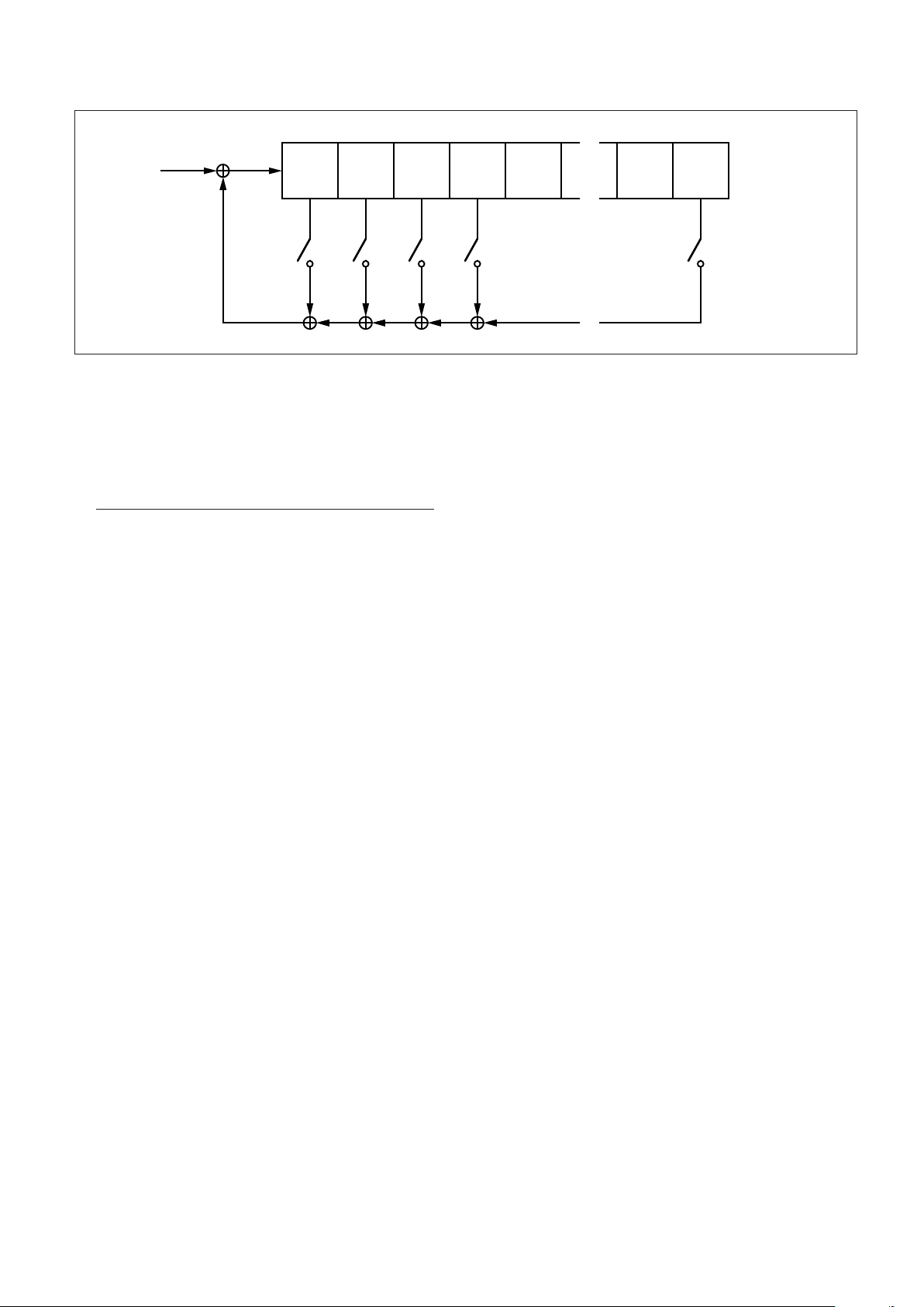
THE HASHING FUNCTION
One purpose of the Hashing Function is to compress the
variable amount of data bits constituted by the extended
message x into a pre-signature P of fixed length (60 bits). The
device realising the Hashing Function is a 60-bit linear
feedback shift register (LFSR), as shown in Figure 8. The 60
feedback coefficients C0, C1,......,C59 are part of the
Authentication Key.
The LFSR is initialised to the 60-bit value P’ = 1000....000
(where Bit P0 = 1) before the process of each authenticated
TC Segment begins. P will be the value in the LFSR after the
last bit of the variable-length extended message x has been
shifted in. The extended message x (x = [m,l,z]) consists of the
following data elements, placed one after the other in that
order:
- the received message m, i.e., the TC Segment
(variable from 1 to 240 octets) without the
Authentication Tail;
- the received LAC value l, i.e., 4 octets (2 bits of LAC
ID, plus 30 bits of LAC Count);
- three octets of virtual fill z, consisting of 24 zeros.
The purpose of the 24 bits of virtual fill is to ensure that the
Hashing Function is provided with a minimum of data bits. The
24 bits of virtual fill z are generated by the PTD. Note that since
m (the TC Segment) cannot be equal to zero, the total length of
an authenticated TC Segment (i.e., [m,l,s]) cannot be smaller
than 10 octets (Segment Header (1 octet) + Authentication tail
(9 octets)). Anything smaller than 10 octets is rejected as being
too short.
THE HARD KNAPSACK
The purpose of the Hard Knapsack is to ensure that it is not
possible to deduce the presignature P from the signature S.
The Hard Knapsack is based on the concept of the modular
knapsack. It consists of 60 weights (numbered from W0 to
W59, each weight being 48 bits long) and is defined by the
following transformation:
j=59
S' = (∑PjWj) mod 2
48
j=0
where the bits Pj of the presignature P select the
corresponding weights Wj of the knapsack.
The result is the 48-bit knapsack sum S’. The most
significant bit of the sum is called S’0.
THE DELETION BOX
The Deletion Box deletes the 8 least significant bits of the
48-bit knapsack sum S’, i.e., bits S’40 through S’47. The result
is the 40-bit authentication signature S (numbered from Bit 0 to
Bit 39, as for signature s).
THE SIGNATURE COMPARATOR
The Signature Comparator compares the received 40-bit
signature s with the onboard generated 40-bit signature S.
Figure 7: Functional Diagram of the Authentication Processor
Hashing
Function
Hard
Knapsack
P
Deletion
Box
S' Sx
Signature
Comparator
S
s
Signature Valid
m
l
z
TC
Segment
(m, l, s)
Page 17
MA28140
17/72
THE AUTHENTICATION KEY
The Authentication Key consists of:
60 x 48-bit Hard Knapsack Weights = 2880 bits = 360 octets
60 x 1-bit Hashing Function coefficients = 60 bits = 8 octets
Full Authentication Key = 2940 bits = 368 octets
The system includes two such 2940-bit keys:
- a fixed, mission-unique Authentication Key, called the
Fixed Key;
- an in-flight programmable Authentication Key, called the
Programmable Key.
(a) Fixed Key
The Fixed Key is required for start-up and emergency
(recovery) operations. The Fixed Key is stored in the external
ROM as part of the Mission-Specific Data.
(b) Programmable Key
The Programmable Key is required for all normal
operations. The contents of the Programmable Key reside in
the RAM where it can be modified by means of Authentication
Control Commands specifically defined for that purpose. The
format of these Change Programmable Key Block Control
Commands, which are specified in the section on AU Control
Commands (page 18), allows any 5-octet block to be modified
starting at any of the 368 octet boundaries.
The Supervisor
The Supervisor consists of four main parts:
- the Logical Authentication Channel (LAC) Registers;
- the Final Authorisation Function;
- the Control Command Processor;
- the Deletion Function.
They are briefly described in the next four subsections.
THE LAC COUNTERS
A LAC Counter is basically a 30-bit counter which is used
to associate every TC segment with an authentication
sequence number. The purpose of this number is to protect the
system against attacks by ensuring that identical TC segments
will not have the same signature except at very large intervals
of time. The LAC counter is incremented by one every time a
TC segment is successfully authenticated (and only then). The
LAC counter value used for authenticating each TC segment is
uplinked with each signature.
Three LAC Registers are provided:
- one Principal LAC register (LAC ID = 00);
- one Auxiliary LAC register (LAC ID = 01);
- one Recovery LAC register (LAC ID = 10).
Bits 0 and 1 of the LAC are fixed in order to select the LAC
Register to be used for the final authorisation of a TC
Segment. For what concerns the 30 bits of LAC Count (Bits 2
through 31, where the LSB is Bit 31), they are implemented as
follows:
- The Principal and Auxiliary LAC counters have 30 bits.
- The Recovery LAC counter has 8 bits (the LSBs 24-31)
whereas the remaining 22 bits (2-23) are permanently
set to 1.
THE FINAL AUTHORISATION FUNCTION
When the received signature s of a TC Segment compares
with the onboard-generated signature S, the contents of the
received LAC Count field is compared with the contents of the
indicated LAC Register. If both contents are found equal, there
are two cases:
- The TC Segment was transferred on a MAP to be
authenticated with a MAP ID lower or equal to the MAP ID
pointer. In this case, the TC Segment is authorised for
transfer to the Segmentation Layer.
Figure 8: Realisation of the Hashing Function
P (i)
0
C
0
P (i)
1
C
1
P (i)
2
C
2
P (i)
3
C
3
P (i)
59
C
59
x (i)
Page 18

MA28140
18/72
- The TC Segment was transferred on MAP 63 (i.e., MAP
111111), which is dedicated to the transfer of Authentication
Control Commands. In this case, the Control Command
Processor is authorised to further process the TC Segment,
which will never be transferred to the Segmentation Layer.
In both cases, the contents of the indicated LAC Register is
incremented by one.
THE CONTROL COMMAND PROCESSOR
The function of the Control Command Processor is to
execute the special TC Segments called Authentication
Control Commands after being authorised by the Final
Authorisation Function. The formats of the various
Authentication Control Commands are specified in the section
on AU Control Commands next. Any TC Segment not
conforming to the specified formats (i.e., both in length and in
contents) are rejected and reported as not executable.
THE DELETION FUNCTION
The Deletion Function deletes the Authentication Tail of all
TC Segments authorised by the Final Authorisation Function.
The complete authentication process is meant to be
transparent to an observer placed at the receiving end of the
Segmentation Layer.
AU Control Commands
It is necessary to differentiate TC Segments containing the
Authentication Control Commands required to reconfigure the
AU. This is done by allocating the TC Segment Header
contents “all ones” to these particular segments, i.e.:
- Sequence Flags set to 11 (Unsegmented)
- MAP ID set to 111111 (MAP63)
TC Segments containing the Authentication Control
Commands shall always be authenticated. The formats of the
Authentication Control Commands are organised in three
groups as follows:
- One octet of TC Segment Header for all three groups.
- One octet following the Segment Header to specify the
Control Command Identifier
- Zero, four or eight octets of Control Command Data
Field, depending on the group.
Table 2 gives the complete list of Authentication Control
Commands, with Group numbers, Control Command IDs and
Command Names. Table 3 shows the format of the TC
Segment for each Group, complete with Authentication Tail.
Each Control Command is specified in the next subsections.
DUMMY CONTROL COMMAND
The purpose of this command is to serve as NOP (No
Operation) for testing purposes. After being authenticated, this
Control Command will have no effect. However, since the AU
has authenticated the Dummy Segment, the contents of the
LAC Register used during the authorisation process have
been incremented and a telemetry report prepared
accordingly.
SELECT KEY CONTROL COMMANDS
(a) Select Fixed Key
The AU selects the Fixed Key prior to authenticating the TC
Segment:
- If authentication is successful, the Fixed Key remains
selected.
- If authentication is unsuccessful, the key previously in
use remains selected.
(b) Select Programmable Key
The AU selects the Programmable Key for authentication
of the TC Segment:
- If authentication is successful, the Programmable Key
remains selected.
- If authentication is unsuccessful, the key previously in
use remains selected.
LOAD FIXED KEY IN PROGRAMMABLE KEY MEMORY
CONTROL COMMAND
This command reloads the Fixed Key set in the
Programmable Key memory with a single command
instruction. The key used for authenticating the TC Segment
containing the Control Command will be whatever key was
selected in the AU at the time the command was transmitted.
SET NEW LAC COUNT VALUE CONTROL COMMAND
The purpose of this Control Command is to set the value of
one of the three programmable LAC Counters: Principal,
Auxiliary or Recovery with LAC Identifiers 00, 01 and 10
respectively. If the LAC Identifier is set to 11, the command is
not executed and reported as not executable. As soon as the
TC Segment is authorised by the authentication process, the
specified LAC Count value is forced into the selected LAC
Register. Note that the 22 MSBs of the 30-bit Recovery LAC
Register are permanently set to all ones, therefore those same
bits in a Set New Recovery LAC Count Value Control
Command are ignored by the AU. The key used for
authenticating the TC Segment containing the Control
Command will be whatever key was selected in the AU at the
time the command was transmitted.
Page 19

MA28140
19/72
Table 2: List of Authentication Control Commands
1 octet 1 octet 9 octets
Segment Header Control Command Identifier Authentication Tail
11111111 00000*** LAC+Signature
Group 1 Control Command, 11 Octets
1 octet 1 octet 4 octets 9 octets
Segment Header Control Command
Identifier
LAC value to be set Authentication Tail
11111111 00001001 LAC ID 2 bits LAC Count 30 bits LAC + Signature
Group 2 Control Command, 15 Octets
Group 3 Control Command, 19 Octets
Table 3: Formats of Authentication Control Commands (Full TC Segment)
1 octet 1 octet 1 octet 7 octets 9 octets
Segment Header Control Command
Identifier
Start Address of
new 40 bit Keyblock
Key specific pattern
to be encoded
Authentication Tail
11111111 0000101* LAC+Signature
GROUP CONTROL COMMAND
IDENTIFIER (8 BITS)
COMMAND NAME
GROUP 1
0000 0000
0000 0101
0000 0110
0000 0111
DUMMY
SELECT FIXED KEY
SELECT PROGRAMMABLE KEY
LOAD FIXED KEY IN PRO GRAMMABLE KEY MEMORY
GROUP 2 0000 1001 SET NEW LAC COUNT V ALUE
GROUP 3
0000 1010
0000 1011
CHANGE PROGRAMMABLE KEY BLOCK A
CHANGE PROGRAMMABLE KEY BLOCK B
Page 20

MA28140
20/72
CHANGE PROGRAMMABLE KEY BLOCK CONTROL
COMMANDS A AND B
Two such Control Commands are provided to cover the full
size of the Programmable Key:
- Command A concerns the first 256 octet boundaries.
- Command B concerns the last 112 octet boundaries.
It is possible to load a 5-octet (40 bits) block starting from
any of the 368 octet boundaries. Any transmission using the
unused boundaries of Command B (from 113 to 255) is
ignored and reported as non-executable. The key used for
authenticating the TC Segment containing one of these
Control Commands will be whatever key was selected in the
AU at the time each Control Command was received. Once the
TC Segment has been authorized by the authentication
process, the TC Segment, minus the 40-bit signature s (i.e.
[m,l]) is complemented and passed once more through the
signature-building process, i.e. through the Authentication
Processor. The 24 bits of virtual fill z are inserted as before,
i.e., they are not complemented, but remain all zeros. The
result of the process is a 40-bit pseudo-signature which,
instead of being sent to the Signature Comparator, is loaded in
the Programmable Key memory, starting at the octet location
indicated by the start address field, as follows:
- Bits 32 through 39 of pseudo-signature at the indicated
octet location;
- Bits 24 through 31 of pseudo-signature at the next
location (start address + 1);
- And so on, until Bits 0 through 7 are loaded at location
start address + 4.
Any arbitary procedure can be used for changing the key,
starting from any of the 368 octet boundaries.
Figure 9: Organisation of the Programmable Key Memory
W0 (40 to 47)
40 47
000200
W0 (32 to 39)
32 39
001201
W0 (24 to 31)
24 31
002202
W0 (16 to 23)
16 23
003203
W0 (8 to 15)
815
004204
W0 (0 to 7)
07
005205
W1 (40 to 47)
40 47
006206
W1 (32 to 39)
32 39
007207
W42 (16 to 23)
16 23
2552FF
W42 (8 to 15)
815
000300
W59 (0 to 7)
07
103367
C (59 to 56)
59 56
104368
C (55 to 48)
55 48
105369
C (47 to 40)
47 40
10636A
C (39 to 32)
39 32
10736B
C (31 to 24)
31 24
10836C
C (23 to 16)
23 16
10936D
C (15 to 8)
15 8
11036E
C (7 to 0)
70
11136F
RAM
Mapping
Address provided in the
Control command (decimal)
Bank ABank B
Note: Bit 0 is the MSB
Page 21
MA28140
21/72
4.4 SEGMENTATION LAYER
Overview of the Layer
The segmentation layer provides the means to distribute
several distinct streams of variable-length data units (e.g. the
TC packets) to different applications by providing a number of
service access points called the Multiple Access Points
(MAPs). The data flow on each stream can be controlled by the
receiving application using handshake control.
A TC segment consists of three distinct protocol data
elements:
- an 8-bit segment header, the purpose of which is to
identify the MAP connection and flag the sequential
position of the segment relative to the complete TC
Packet,
- a segment data field, of maximum length 248 octets,
which contains all or a portion of a TC Packet,
- the 9-octet Segment Trailer specific to authenticated
segments is removed by the authentication layer.
Standard Data Structures Within the Layer
The structure of the TC segment is given below:
Segment Header
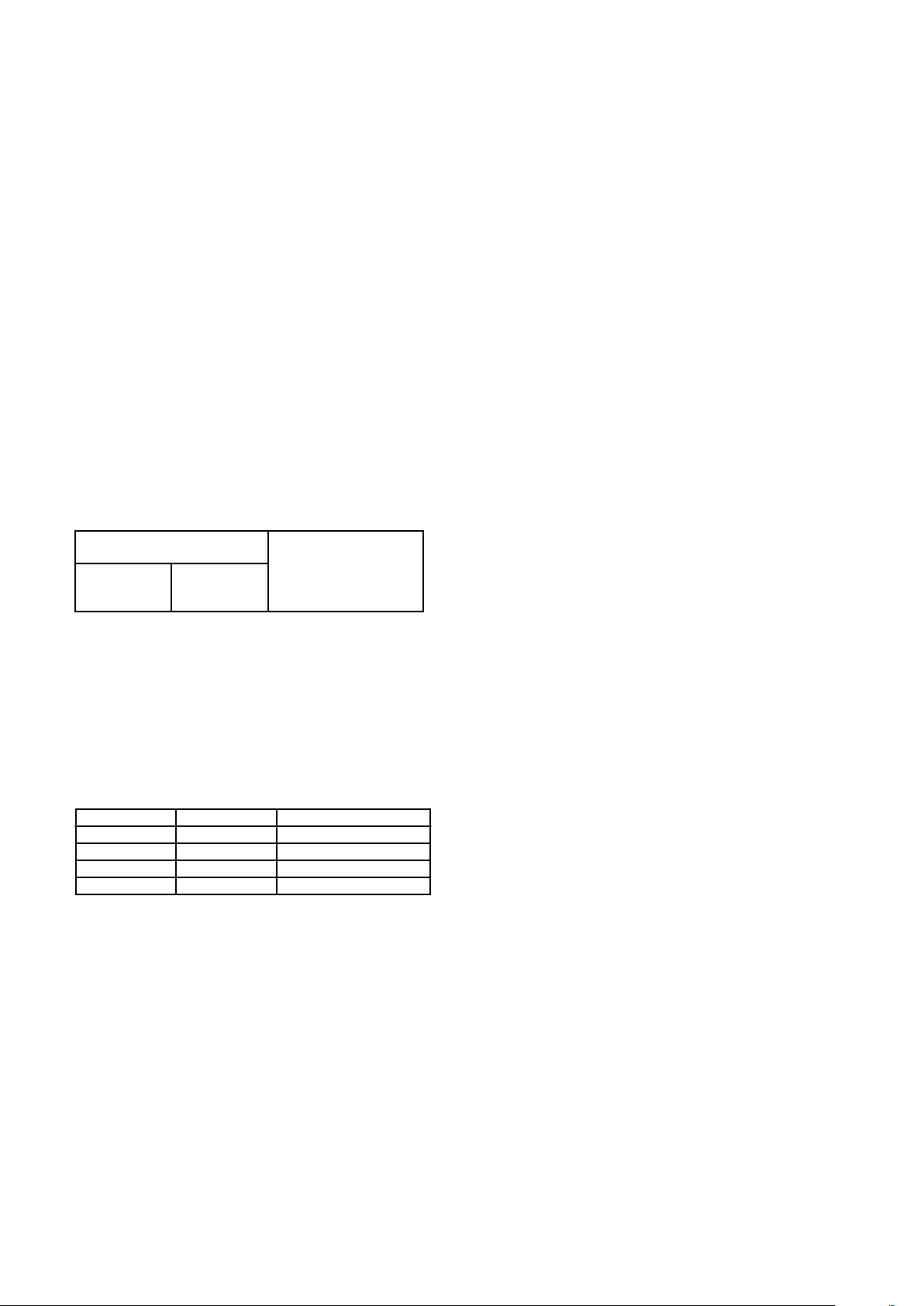
The Segment Header is the first octet (octet 0) of the TC
segment structure. The Segment Header is divided into two
major fields as follows:
- Sequence Flags (bits 0 & 1): this field is used by the
segmentation protocol to indicate the sequential position
of the segment relative to the complete data unit (e.g. the
TC Packet). The flags are interpreted as follows:
When the flags are set to 11 this means that the TC
Segment Data Field contains an entire TC Packet. Except for
the CPDU described in section 4.5, these flags are ignored by
the PTD.
- Multiplexed Access Point (MAP) Identifier: this 6-bit field
enables up to 64 MAP connection addresses to be associated
with a single Virtual Channel. The PTD supports MAP 1 to 63
as externally available MAPs. MAP 0 is dedicated to the
CPDU. MAP 63, when AU is enabled, is reserved for AU
commands; when the AU is disabled, MAP 63 is processed by
the segment layer like a standard MAP (see section 4.3).
Bit 0 (MSB) Bit 1 Interpretation
0 1 First segment
0 0 Continuation segment
1 0 Last segment
1 1 Unsegmented
Segment Data Field
The segment data field may vary from 0 to 248 octets
maximum. When the optional Segment Trailer is used, the
maximum length of the segment data field will be reduced by 9
octets.
Standard Procedures Within the Layer
The following segmentation layer functions are
implemented in the PTD:
- the back-end buffer for the accepted TC segment. The
back-end buffer is shared between the Transfer Layer
and the Segmentation Layer.
- the MAP interface.
Upon reception of a new segment the Segment Layer
performs the following operations:
- Checks whether the segment is authenticated or not.
- Starts the AU process if the segment is authenticated
and if the AU is not disabled. The Segment Layer waits
for the completion of the AU process (internal or external).
A security mechanism is implemented, in case of AU
locking mechanism the user can stop the AU process by
activating the AU disable signal. In this case, the segment
layer stops waiting for the AU completion process and the
content of the back end buffer is lost.
- Checks if the frame is a CPDU command (MAP 0). In
this case, the CPDU layer is activated and no data is
output on the MAP interface.
- Checks if the frame is an AU command (MAP 63) and
the AU is not disabled. In this case no data is output on
the MAP interface.
- For a MAP 1 to 62 and for MAP 63 if the AU is disabled,
the data is provided in serial or in parallel via the MAP
interface. The MAP output frequency for serial MAP is
selectable by reading a value associated with each MAP
in the external ROM (see section 5.2).
SEGMENT HEADER
SEGMENT DATA
FIELD
Sequence
Flags
2 bits
MAP
Identifier
6 bits
variable
<--------------- 1 octet ------------><- from 0 to 248 octets ->
Page 22

MA28140
22/72
4.5 COMMAND PULSE DISTRIBUTION UNIT
General Requirements
The CPDU is a simple unit that is solely accessible from
ground. The aim of this unit is to generate pulses to drive
certain actuators (e.g. relays). The CPDU is identified by the
Application Process Identifier placed in the TC Packet Header.
The Application Identifier of the CPDU is programmable in
ROM at addresses 006 and 007.
Functional Description
The CPDU receives TC segments, each segment
containing a complete TC Packet. TC segments having a MAP
equal to zero are carrying CPDU commands. It must be noted
that if the internal AU is enabled, MAP0 segments are always
authenticated. When a new segment carrying CPDU
commands has arrived, two cases are possible:
- the CPDU is still executing previous CPDU commands. In
this case, the incoming TC segment is ignored, whether it was
transferred in an AD or BD transfer frame.
- the CPDU is idle. The incoming TC segment is copied
from the back end buffer to the CPDU buffer for checking and
execution by the CPDU.
An important point must be noted: there is no packetisation
layer abort command associated with the CPDU. Once it has
accepted a TC Packet, the CPDU cannot release it until all
command instructions specified in that packet have been
executed.
The CPDU performs first the clean validation process
which verifies the complete packet (CRC, packet length,
segmentation flags). If the clean validation process is
successful, the CPDU performs the legal validation process,
which checks the content of the Packet Headers. The result of
the two previous verifications is reported in the 16 bits CPDU
status. For a dirty or illegal CPDU Packet, the CPDU buffer is
erased. The execution of the CPDU commands is possible
only if all the verifications succeed.
Checking the CPDU-Specific TC Packet
The CPDU Packet format is shown below:
A short description of the fields of the CPDU Packet is
given below:
- version number: 3-bit field occupying the 3 MSBs of the
packet header. To be compliant with ref.1, these 3 bits should
be 000.
- type bit: this bit identifies if the Packet is telemetry type
(type bit = 0) or telecommand type (type bit = 1). To be
compliant with ref 1, this bit should be set to 1.
- data field header flag: this indicates the presence (data
field header flag = 1) or absence (data field header flag = 0) of
a data field header within the packet data field. To be
compliant with ref 1, this bit should be set to 0.
- application process identifier: this field identifies the
particular process to which the CPDU Packet is sent.
- sequence flags: this two-bit field indicates if the packet is
a first, last or intermediate component of a higher layer data
structure. For CPDU Packets, these two bits shall be equal to
11.
- packet sequence count: this 14-bit field allows a particular
TC Packet to be identified with respect to others occurring
within a telecommand session. This field is reported in the
CPDU status for clean and legal CPDU packets.
- packet length: this field specifies the number of octets
contained within the packet data field, by indicating the number
of octets in data field minus 1.
- packet data field: this field contains the CPDU commands
and the CRC for packet error control.
PACKET HEADER (48 bits) PACKET DATA FIELD
(variable)
PACKET IDENTIFICATION PACKET
SEQUENCE
CONTROL
PACKET
LENGTH
DATA
FIELD
HEADER
APPLIC-
ATION
DATA
PACKET
ERROR
CON-
TROL
version
number
3
type 1data field
header
flag
1
applicat-
ion
process
ID
11
Sequence
Flags
2
Packet
Name or
Sequence
Count
14
16 16 16 variable variable 16
Page 23

MA28140
23/72
The CPDU Packet is checked in two steps: the clean
validation process and the legal validation process. The clean
verification process performs the following tests:
- correct CRC (last two octets of the Packet contain a 16-bit
CRC calculated using the same algorithm as used for the TC
transfer frame, see section on transfer frame) to verify that
there is no error in the Packet.
- the TC Segment Segmentation Flags (in Segment
Header) are equal to 11.
- the CPDU Packet length is checked to be an even
number of octets, greater than or equal to 10 octets and less
than or equal to 248 octets: 10 octets ≤ TC Packet length =
even number of octets ≤ 248 octets. The CPDU Packet length
is read from Packet Header octets 5 and 6.
- consistency between the actual number of octets making
up the CPDU Packet and the Packet length field. To achieve
this, the Packet Header octet 5 is checked to be zero and the
Packet Header octet 6 is checked to be consistent with the
effective packet length.
At this level, if the packet is found to be error-free, it is
declared clean and the process continues. Otherwise, the
complete CPDU packet is erased.
The legal verification process performs the lollowing tests
on the Packet Header (see ref 1, Section 8):
- the first octet of the Packet Header (version number &
type bit & data fields header flag & 3 MSBs of Application
Process Identifier) is compared with the value programmed in
ROM at address 006.
- the second octet (8 LSBs of Application Process
Identifier) is compared with the value programmed in ROM at
address 007.
- in the third octet (sequence flags & 6 MSBs of packet
name or sequence count), only the sequence flags field is
checked by the PTD to be equal to 11. The packet name or
sequence count is not verified, it is only reported in the CPDU
status.
- the fourth octet (8 LSBs of packet name or sequence
count) is not tested since the packet name or sequence count
is not verified. It is only reported in the CPDU Status.
If the above check succeeds, the TC Packet is declared
legal and its Application Data (command instructions) read out
and executed as described in the next subsection. If the check
fails, the Packet is erased.
Processing the Application Data
The CPDU receives a segment from the segment layer and
stores it for further processing in the CPDU buffer provided in
RAM. At the same time, the clean process is performed. This
segment duplication is necessary due to delayed command
execution. The duration of the transfer is equal to:
Td = Nb * Tacc
where Nb is the number of octets of the TC segment
(including AU tail), and Tacc is the duration of three RAM
accesses Read - Write - Read (the last read is used for
computing the CRC with data effectively stored in RAM). Tacc
can be estimated to 20*Tck (5 µs for a clock frequency of 4
MHz).
The application data of the CPDU packet should consist of
at least one command instruction in the form of one double
octet, or several of such double-octet command instructions,
up to the maximum capacity.
Each double octet should be formatted as follows:
• first octet: specifies one of 256 Command Pulse outputs.
The command distribution shall be made by an external
demultiplexer (256 possible command pulse outputs).
• Second octet: specifies the duration of the Command
Pulse to be issued on the specified output as follows:
- the 5 MSBs are ignored by the CPDU,
- the 3 LSBs specify the duration of the Command
Pulse, which is equal to about 2
X
multiplied by D
where X is the value of the 3 LSBs and
D = 40960 clock periods for CPDUDIV=0,
D = 8192 clock periods for CPDUDIV=1.
(see section 5.5 for exact figures.)
When there is more than one command instruction in the
CPDU Packet, each instruction is executed one after the other
in the same sequence as in the packet.
The maximum capacity of the CPDU packet is:
• 248 octets corresponding to 120 command instructions if
the Internal or External Authentication Unit is disabled
(AUDIS=1) or if the External Authentication Unit is enabled
(AUEXT=1 and AUDIS=0) and AUTSL=1.
• 238 octets corresponding to 115 command instructions if
the Internal Authentication Unit is enabled (AUEXT=0 and
AUDIS=0) or if the External Authentication Unit is enabled
(AUEXT=1 and AUDIS=0) and AUTSL=0.
For the calibrated pulses being output on the CPDUEN pin,
the pulse amplification shall be made by external hardware.
The CPDU provides a 16 bit status, CPDUS, that can be
fetched by the telemetry system. The different fields of the
CPDU status are detailed later.
Page 24

MA28140
24/72
4.6 TELEMETRY REPORTING
General Description
Telemetry reporting is essential to the normal operation of
the telecommand data communication system.
Data Reports are not modified during telemetry readout. In
particular they are not affected by the arrival of new report
data. If the telemetry interface sampling rate is slower than the
rate at which new data reports are generated, a double register
mechanism ensures that the complete data report is read out.
CLCW Status Report
The Command Link Control Word (CLCW) is a standard
reporting data structure of the Packet Telecommand System. It
is a four-octet word generated by the spacecraft, the PTD
generating only the 2 least significant octets of this CLCW
which are described hereafter.
Bits Value Meaning
0 (MSB) No RF Available
1 No Bit Lock
2 Lock Out
3 Wait
4 Retransmit
5,6 FARM B Counter
7 0 Report Type
8 - 15 (LSB) Report Value
Each CLCW field is specified in the next paragraphs:
• No RF Available. This field is dedicated to the Physical
Layer, i.e. the RF Transponders. When this field is 1, the
RF physical connection is not available through any of the
spacecraft transponders. When it is 0, the RF connection is
available through at least one of the spacecraft
transponders. This information is provided to the PTD by
an input pin called RFAVN.
• No Bit Lock. This field is dedicated to the Physical layers,
and monitors the presence of the spacecraft
demodulation. When this field is 1, all the TC Active Signals
(0 to 5) are zero at the PTD input pins. When it is 0, at least
one of the TC Active signals is set to 1.
• Lockout Flag. If 1, this field indicates that the FARM- 1 is
in the Lockout state.
• Wait Flag. If 1, this field indicates that the FARM- 1 is in a
Wait state.
• Retransmit Flag. If 1, this field indicates that an AD frame
has been lost in transmission or has been discarded
because there was no buffer space available.
• FARM B counter. This 2 bit field contains a wraparound
up-counter (modulo 4) of each TC frame of type BC or BD
declared valid by the Legal Frame Validation process, and
therefore acceptable by the FARM-1.
• Report Type. In the PTD it is always 0 in accordance with
reference 1.
• Report Value. This field is maintained by the FARM-1 and
contains the next expected frame sequence number V(R).
The first bit to be read in serial mode is Bit 0 (MSB). The
interface for reading the CLCW status is specified in
section 5.3.
CPDU Status Report
The CPDU Status report consists of 16 bits of status data
formatted as follows:
Bits Value Meaning
0,1 00 Cold Start
01 Last TC Packet accepted legal
10 Last TC Packet accepted clean,
but erased as not legal
11 Last TC Packet erased as not
clean
2 - 15 (LSB) all 1 Cold Start
all other Packet Sequence Count (or
values Name) of last legal CPDU
Packet
The first bit to be read out in serial mode is Bit 0 (MSB).
Legal and Clean concepts are defined previously. The
telemetry interface used to read out the CPDU Status Report is
fully described in section 5.3.
AU Status Report
The AU Status Report consists of 80 bits (i.e. 10 octets) of
status data formatted as follows:
Bits Value Meaning
0,1 00 Permanently set to 00
2 - 31 Current value of the contents of
the Principal LAC counter. The
LSB of the LAC counter value is
in bit 31
32,33 01 Permanently set to 01
34 - 63 Current value of the contents of
the auxiliary LAC counter. The
LSB of the LAC counter value is
in bit 63
64 Key in use by AU:
0 fixed key in use
1 Programmable key in use
65 - 71 0000000 Permanently set to 0 (reserved
for future use)
72 - 79 (LSB) Current value of the 8 LSBs of
the recovery LAC counter. The
LSB of the LAC counter value is
in bit 79.
The first bit to be read in serial mode is bit 0 (MSB).
The AU Status report is implemented by using a double
register mechanism located in the external RAM. In the case of
external AU, the external AU can write the AU Status in RAM.
The number of the buffer is given by the AUS pin and the
toggling mechanism of the AU Status buffer is locked by the
PTD when the signal AUST ( External AU Start) is high. The
telemetry interface used to read the AU status report is
described in section 5.3.
Page 25

MA28140
25/72
Frame Analysis Report
The FAR is required for proper testing and check-out of the TC Decoder. The FAR consists of 32 bits of survey data formatted
as follows:
BI TS VALUE MEANING
0 (MSB)
1,2,3
4,5,6
7 - 12
13,14,15
16,17
18,19,20
21 - 26
27
28,29,30
0
1
000
001
010
011
100
101
110
111
000
001
010
011
100
101
110
111
xxxxxx
xxx
00
01
10
11
xxx
xxxxxx
0
000
001
010
011
STAT U S OF SU R VEY D AT A
New survey data (or Cold Start)
Old survey data
FR AM E AN ALYSIS
Note: The report of the lowest rank (i.e. of lowest 3-bit value) has
precedence in case of conflicting states.
Abandoned CLT U (see Note 1)
Fram e declared dirty
Fram e declared illegal for one reason
Fram e declared illegal for multiple reasons
Fram e (AD ) discarded because of LOC KOU T
Fram e (AD ) discarded because of W AIT
Fram e (AD ) discarded because of N (S) or V(R )
Fram e (AD , BD or BC ) Accepted by FARM -1
LEGAL/ILLEGAL FR AM E QU ALIFIER
Note: When a frame is declared ILLEGAL for multiple reasons,
only the reason of the first rank (i.e. of lowest 3-bit value) is
reported. The fields mentioned are those of the frame header.
No illegal report (or Cold Start)
Error in fixed fields (Version & Reserved)
Illegal combination (AC) of Bypass & Control Com m and F lags
Wrong Spacecraft ID
Wrong VC ID (because of Bits 0 to 4 of ID)
Wrong VC ID (because of Bit 5 of ID)
N(S) of BC or BD frame not set to all 0
Wrong BC frame data format (not executable)
COUNT OF ACCEPTED CODE BLOCKS PER C LT U
Straight 6-bit binary count of correct or single-error-corrected
codeblocks in one C LT U ; (Cold Start value: 000000)
COUNT OF SINGLE-ERR OR C OR R EC T IONS PER C LT U
Straight 3-bit binary count, saturates at maximum value, no roll
over. (Cold Start value:000)
LEGAL FR AM E QU ALIFIER (4 ST AT ES)
AD frame
No report on legal frame (or Cold Start)
BD frame
BC frame
SELECT ED C H AN N EL INPU T (M AXIMUM CAPABILITY : 6
INPUTS)
(Cold Start value : 111)
LAST M AP AD D R ESSED (64 M APS)
(Cold Start value : 111111)
RESER VED BY ESA (set to 0)
AUTHENTICATION PROCESS ANALYSIS
No authentication report (or C old Start)
AUTHORISED SEGMEN T QU ALIFIER
Authorised data segm ent
Authorised (and executable) Authentication Control Com m and
Authorised dumm y segment received
Page 26

MA28140
26/72
A few specific points need to be detailed:
Note 1: The abandoned CLTU state (000) is used to
indicate:
• the Cold Start
• a first TC codeblock of CLTU was abandoned (erased)
because of event 4 or event 2
• an event E2(a) channel deactivation occurs (see section
4.1)
• an event E2(b) CLTU error occurs (see section 4.1)
In the case of an Abandoned CLTU the Legal/lllegal
Frame Qualifier (bits 4, 5, 6) is set to 000 and the Legal
Frame Qualifier (bits 16, 17) is set to No Report on Legal
Frame (01).
Note 2: The rejected segment qualifier in the
Authentication process analysis has the following
prioritisation:
• 111 Too short TC segment has the highest precedence,
followed by
• 100 Error in Signature, followed by
• 101 Error in LAC, followed by
• 110 Wrong format of AU command or segmentation
flags.
The FAR is sampled and read by a telemetry interface
described in section 5.3.
BI TS VALUE ME ANING
31 (LSB)
100
101
110
111
0
REJECT ED SEGM EN T QU ALIFIER
Error in Signature
Error in LAC
Wrong format (not executable) of authorised Authentication
Control Com m and (includes Segment Header)
Wrong length of TC Segm ent prior to being authenticated
(authorised), i.e. length shorter than 10 octets
set to 0
Page 27

MA28140
27/72
5. PTD INTERFACES
5.1 PHYSICAL CHANNEL INTERFACE
Each TC channel consists of 3 input lines:
• TCC
i
: symbol clock input
• TCS
i
: symbol stream input (NRZ-L)
• TCA
i
: channel active indication input
The maximum symbol rate with guaranteed operation
(using the internal AU) on these channels is 50 kbps. For
higher frequency, an incomplete AU process may occur
resulting in wrong signature calculation and thus rejected
frames. Without AU the symbol rate could be 200 kbps (not
guaranteed). At higher frequency, incorrect processing may
occur due to insufficient time to perform memory accesses.
The interface is composed of 6 TC channels. Figure 10 below
gives the timing associated with one of these 6 channels. For
unused channels, the TCAi signal should be connected to VSS,
and the TCCi and TCSi signals to VDD.
The DECOD output is activated when the CLTU decoder
state machine is in the decode state (see section 4.1). This
output goes high following the detection of a start sequence,
and goes low following a codeblock rejection or CLTU error.
5.2 MAP INTERFACE
The MAP interface allows the PTD to provide the on-board
applications with the TC segments stored in the back-end
buffer in the RAM. It is possible to transfer full TC segments
(including segment header and packet segment) with various
lengths, from 1 octet to 249 octets. The first data output is the
TC segment header. It is possible for an application to use
either a serial or parallel interface to read this TC data. The
choice between serial or parallel interface is made with the
configuration input pin PAR as follows:
• PAR = 1; the parallel MAP interface is used (section 5.4)
• PAR = 0; the serial MAP interface is used
The serial MAP interface consists of 5 signals.
• MAPDSR, data set ready output,
• MAPDTR, data terminal ready input,
• MAPCK, MAP clock output,
• MAPDATA, segment data output,
• MAPADT, aborted data transfer output.
Figure 10: TC Channel Input Timing
Page 28

MA28140
28/72
In addition, the MAP interface provides the output signal
MAPSTN, in order to save the MAP identifier present on the
local data bus (LDAT<7..0>) in an external latch. This MAP
identifier is used to demultiplex the segment data toward the
selected application. The MAPSTN signal can be controlled by
the LACK signal. MAPDSR has no effect when MAPDTR
output is deasserted.
The output frequency for each MAP is programmable and
is defined in ROM. For MAP number n, the address of the
value X defining the MAP frequency is (hex) 100+n. The MAP
output frequency is given by F=f
ck
/[2X], (X is coded on the 4
LSBs and its value varies from 1 to 13; for other values, the
output frequency is F = fck/2). For example for a PTD clock
frequency of 4 MHz, setting the ROM value to 4 will generate a
MAP frequency of 250 kHz. With a system clock frequency fck
of 4 MHz, the MAPCK frequency can vary from 488 Hz (X=13)
to 2 MHz (X=1). The use of a too low MAP frequency
compared to the TC clock frequency may lead to the activation
of the WAIT flag if the MAP output of a previous frame is not
finished when a new segment arrives. As a rule of thumb, in
order to avoid the Wait flag being asserted, the MAP frequency
should be at least the TC input bit rate multiplied by 10 when
fully variable segment size (by 2 if fixed length).
Figure 11 describes the serial interface in three different
transfer situations.
MAPDSR
MAPDTR
MAPCK
MAPDATA
MAPADT
PTD APPLICATION
PAR = 0
Serial MAP Interface
Note: The bit 0 is the MSB and shall be transmitted first.
Figure 11: Serial MAP Interface
N maximum value is 1991 corresponding to a
TC segment of 249 octets.
Page 29

MA28140
29/72
Example of data transfer with data flow control.
N maximum value is 1991 corresponding to a
TC segment of 249 octets.
Note: For each MAPDTR pulse one octet is transferred.
Note: The MAPADT signal is asserted on octet boundaries of the MAP data being transferred.
Figure 11: Serial MAP Interface (continued)
Page 30

MA28140
30/72
5.3 TELEMETRY INTERFACE
The Telemetry interface allows four different reporting
words to be retrieved.
• the Command Link Control Word (CLCW),
• the Command Pulse Distribution Unit Status (CPDUS),
• the Frame Analysis Report (FAR),
• the Authentication Unit Status (AUS).
It is possible for an application to use either a serial or
parallel interface to read these reports. The selection between
serial or parallel interface is made with the configuration input
pin PAR as follows:
• PAR = 1; the parallel TM interface is used
• PAR = 0; the serial TM interface is used
The parallel interface is described in section 5.4. The
parallel interface is useful for integrating subsystems
comprising both the TC decoder and a processor, without
cross-coupling after the TC decoders. The CLCW has its own
serial telemetry interface which is redundant in serial mode.
The other three reports (CPDUS, FAR, AUS) can be
fetched through a common serial interface (clock and data
lines) using two or five different sample signals. The selection
between using two or five sample signals is made with the
configuration input pin TMMOD as follows:
• TMMOD = 0; the status (CPDUS, FAR, AUS) reports
are fetched with 5 sample signals.
• TMMOD = 1; the status (CPDUS, FAR, AUS) reports
are fetched with 2 sample signals.
Both interfaces use the same TMC and TMD signals.
When the parallel interface is selected it is not possible to use
the TM (and MAP) serial interface, except for the CLCWB
interface which can be used in a serial mode even if the PAR
signal is set to 1. The protocol for the serial interface is fully
compliant with section 4.3 of TTC-B-01 (serial 16 bit digital
channel).
Serial CLCW Interface
The 16 bit Command Link Control Word (CLCW) can be
retrieved through this interface. The serial CLCW interface is
redundant in order to allow two separate redundant TM
encoders to be connected to each TC decoder. Figure 12
shows the serial CLCW telemetry interface. The serial
interface is implemented with 3 signal lines:
• CLCWSA: status sample input,
• CLCWCA: status clock input,
• CLCWDA: status data output.
The redundant serial CLCW interface is identical with the
nominal serial CLCW interface using the 3 signals:
• CLCWSB: status sample input,
• CLCWCB: status clock input,
• CLCWDB: status data output.
Note: The 0 bit is the MSB and is transmitted first.
Figure 12: Serial CLCW Telemetry Interface
CLCWSA
CLCWCA
CLCWDA
PTD
APPLICATION
Telemetry
Systems
PAR = 0
CLCW Serial Interface
CLCWS I/F
Page 31

MA28140
31/72
CPDU Status Report Interface in 5 Samples Mode
The 16 bit Command Pulse Distribution Unit Status report
can be retrieved through this interface. It is possible for an
application to use either a serial or a parallel interface to read
out this status report. The serial or parallel mode is selected
with the PAR configuration pin of the PTD (see section 5.4).
The serial interface in 5 samples mode uses 3 signal lines:
• CPDUS: status sample input.
• TMC: status clock input, is also used for FAR and AUS.
• TMD: status data output, is also used for FAR and AUS.
The sample signal CPDUS needs to be activated only once
to fetch the entire CPDUS word. CPDUS, FAR1S, FAR2S,
AUS1S and AU2S cannot be asserted simultaneously. If
CPDUS, FAR1S, FAR2S, AUS1S and AU2S are not asserted,
activating the TMC signal will generate invalid data on the
TMD output. If the CPDU status report interface is not used,
the CPDUS signal should be connected to V
DD
. Figure 13
below describes the CPDU telemetry serial interface.
Serial FAR Status Report Interface in 5 Samples
Mode
The 32 bit Frame Analysis Report can be retrieved through
this interface. It is possible for an application to use either a
serial or a parallel interface to read out this status report. The
serial or parallel mode is selected with the PAR configuration
pin of the PTD (see section 5.4). The serial interface in 5
samples mode uses 4 signal lines:
• FAR1S: first status sample input,
• FAR2S: second status sample input,
• TMC: status clock input, is also used for CPDUS and
AUS,
• TMD: status data output, is also used for CPDUS and
AUS.
The sample signal CLCWSA should be activated only once
to fetch the entire CLCW word. The serial CLCW interface has
been designed to allow the VCM device specified in reference
3 to automatically retrieve the CLCWs without any additional
components being required. If one of the CLCW interfaces is
not used, the following signals CLCWSx and CLCWCx should
be connected to V
DD
. Activating the CLCWCA (CLCWCB)
signal when CLCWSA (or CLCWSB) is deasserted, will
generate invalid data output on CLCWDA (or CLCWDB).
Note: The 0 bit is the MSB and is transmitted first.
Figure 13: CPDU Telemetry Serial Interface
CPDUS
TMC
TMD
PTD
APPLICATION
Telemetry
Systems
PAR = 0
CLCW Status Report Serial Interface
CPDUS I/F
Page 32

MA28140
32/72
The sample signals FAR1S and FAR2S should be
asserted to fetch the 32 bits of FAR. CPDUS, FAR1S, FAR2S,
AUS1S and AU2S cannot be asserted simultaneously. If
CPDUS, FAR1S, FAR2S, AUS1S and AU2S are not asserted,
activating the TMC signal will generate invalid data on the
TMD output. If the FAR status report interface is not used, the
FAR1S and FAR2S signals should be connected to V
DD
.
Figure 14 describes the FAR telemetry serial interface.
Serial AU Status Interface in 5 Samples Mode
The 80 bit Authentication Unit Status report can be
retrieved through this interface. It is possible for an application
to use either a serial or a parallel interface to read out this
status report. The serial or parallel mode is selected with the
PAR configuration pin of the PTD (ee section 5.4). The serial
interface in 5 samples mode is implemented with 4 signal lines:
• AU1S: first status sample input,
• AU2S: second status sample input,
• TMC: status clock input, is also used for CPDUS and
FAR.
• TMD: status data output, is also used for CPDUS and
FAR.
When AU1S is asserted, the pointer for reading out data
with AU2S is reset to the second octet of the report. The
sample signals AU1S and AU2S should be asserted as
described in Figure 15 to fetch the 80 bits of AUS report.
CPDUS, FAR1S, FAR2S, AUS1S and AU2S cannot be
asserted simultaneously. If CPDUS, FAR1S, FAR2S, AUS1S
and AU2S are not asserted, activating the TMC signal will
generate invalid data on the TMD output. If the AU status
report interface is not used, the AU1S and AU2S signals
should be connected to V
DD
.
Figure 15 describes the AUS telemetry serial interface.
Serial CPDU, FAR, AU Status Interface in 2
Samples Mode
The 16 bit Command Pulse Distribution Unit status report,
the 32 bit Frame Analysis report and the 80 bit Authentication
Unit status report can be retrieved through this interface. The
serial interface in 2 samples mode is implemented with 4
signal lines:
• CPDUS: first status sample input,
• FAR1S: second status sample input,
• TMC: status clock input,
• TMD: status data output.
Note: The 0 bit is the MSB and is transmitted first.
Figure 14: FAR Telemetry Serial Interface
FAR1S
FAR2S
TMC
TMD
PTD
APPLICATION
Telemetry
System
PAR = 0
FAR Status Report Serial Interface
FAR I/F
0 1 2 3 4 5 6 7 8 9 10 11 12 13 14 15
16 17 18 19 20 21 22 23 24 25 26 27 28 29 30 31
Page 33

MA28140
33/72
Note: The 0 bit is the MSB and is transmitted first.
Figure 16: Telemetry Serial Interface in 2 Sample Mode
Note: The 0 bit is the MSB and is transmitted first.
F
igure 15: AUS Telemetry Serial Interface
AU1S
AU2S
TMC
TMD
PTD
APPLICATION
Telemetry
System
PAR = 0
AU Status Report Serial Interface
AU I/F
bit 0-15
bit 16-31
bit 32-47 bit 48-63
bit 64-79
0
31
0
79
CPDUS
FAR1S
TMC
TMD
PTD
APPLICATION
Telemetry
System
PAR = 0
Telemetry Report Serial Interface in 2 Samples Mode
Page 34

MA28140
34/72
When CPDUS is asserted, the pointer for reading out data
with FAR1S is reset to the first octet of the FAR. The samples
CPDUS and FAR1S should be activated as described in
Figure 16 to fetch the 128 bits of status words. The first 16 bits
are those of the CPDU status word, to be acquired by asserting
the CPDUS signal line. The next 32 bits are those of the FAR
status word, to be acquired by signalling on the FAR1S signal
line (2 x 16 bits). The last 80 bits are those of the AU status
word, to be acquired by additional assertions (5 x 16 bits) of the
FAR1S signal line. It is possible to read out only the first 48 bits
(CPDU and FAR), e.g. if the AU is not used.
FAR1S, AU1S and AU2S do not have any impact in this
mode, but should be connected to V
DD
.
octet (all bits set to 0) on the 8 LSB. For example, if the TC
segment to be output is (hexadecimal) AABBCC, the first word
read is AABB and the second one is CC00.
After a PCSN assertion, the PRDY output is activated
when the data is available on the PBUS output. The PRDY is
released when the PCSN signal is deasserted. The PRDY
signal will not be asserted if PCSN is asserted and PAD = 000
(MAP segment read) when MAPDSR is inactive. When PCSN
is deasserted the PBUS bus is tristated. The MAP status word
can be read at any time. The access to this word is identical to
the telemetry status word accesses as described in Figure 18.
It contains the following information:
• PBUS<0>: MAPDSR information (identical to MAP data
set ready signal line).
• PBUS<1>: ODD/EVEN segment length information
(Odd: 1, Even: 0).
• PBUS<15..2>: not used (value : 00000000000000).
NOTE: only TC segments appearing on MAP 1 to 62 and
on MAP 63 when AU is disabled, can be read out using this
parallel interface. MAP 0 is not affected by this parallel
interface since it is directly connected to the CPDU. The
telemetry status word is read as described in Figure 18.
The CLCW status word is read using one read cycle where
PAD = 010.
The CPDU status word is read using one read cycle where
PAD = 001.
The FAR status words are read with two read cycles:
• One read cycle with PAD = 100 for the first 16 bits
(FAR1)
• One read cycle with PAD = 101 for the last 16 bits
(FAR2).
The AU status words are read using five read cycles:
• One read cycle with PAD = 110 for the first 16 bits (AU1)
• Four read cycles with PAD = 111 for the last 64 bits
(AU2): bits 16-31, bits 32-47, bits 48-63 and bits
64-79.
When the AU1 Status report is read, the pointer for reading
out data with AU2 is reset to the second octet of the AU report.
The Status of Survey bit is set when FAR2 is read. The
following pins have no influence in parallel mode:
• MAPDTR (should be connected to V
SS
),
• CLCWSA, CLCWCA (should be connected to V
DD
),
• AU2S (should be connected to V
DD
),
• TMC (should be connected to V
DD
),
• TMMOD (should be connected to V
SS
),
The reports and TC segments cannot be read out in an
arbitrary order. The following constraints apply: A FAR2 read
out shall not be separated from the previous FAR1 read out by
AU1 or AU2 read out. An AU2 read out shall not be separated
from a previous AU1 or a previous AU2 read out by FAR1 or
FAR2 read out.
5.4 PARALLEL INTERFACE
A parallel interface is provided on the PTD to access the
TC segment and the four reporting words: CLCW, CPDUS,
FAR and AUS. The parallel mode is selected with the PAR
configuration pin of the PTD (the parallel mode is selected
when PAR is set to 1). The parallel interface is implemented
with the following signals:
• PCSN: parallel bus chip select input,
• PAD<2..0>: parallel address bus (input),
• PRDY: data validation output,
• PBUS<15..0>: parallel data bus (output),
• MAPDSR: MAP data set ready output,
• MAPADT: MAP aborted data transfer output.
The PCSN, PAD2, PAD1 and PAD0 signal lines use
respectively the CPDUS, FAR1S, FAR2S and AU1S input pins
of the serial interface. The application acquires the TC
segment and the four reporting words by read cycles. The
addressing of these words is as follows:
When the AU1 status is read, the pointer for reading out
data with AU2S is reset. The MAP TC segment is read as
described in Figure 17.
A TC segment is read by consecutive accesses to <000>.
Data read when MAPDSR is not asserted is not valid. The TC
segment data octet of even rank is output on the 8 MSB of
PBUS (the first octet is 00 and therefore even). The TC
segment data octet of odd rank is output on the 8 LSB of
PBUS. In the case of a TC segment with an odd number of
octets, the last 16 bits word output on PBUS contains the last
TC segment data octet on the 8 MSB and a non significant
PAD2 PAD1 PAD0 read word
0 0 0 MAP segment
0 0 1 CPDU status
0 1 0 CLCW status
0 1 1 MAP status
1 0 0 FAR1 status
1 0 1 FAR2 status
1 1 0 AU1 status
1 1 1 AU2 status
Page 35

MA28140
35/72
Figure 17: Parallel MAP Interface
Figure 18: Parallel Telemetry Read Cycle
For a 4 MHz clock, the duration D is 10.24 ms if
CPDUDIV=0 and 2.048 ms if CPDUDIV=1. The maximum
duration (=128xD) is about 1.31 s if CPDUDIV=0, and 262 ms
if CPDUDIV=1. The delay between the time at which the
packet has been declared Legal and the execution of the
command instruction (rising edge of CPDUEN) can be any
value between 0.5 D and 1.5 D. The duration between two
instructions placed one after the other in the same CPDU
packet (from falling edge to rising edge of CPDUEN)
corresponds to about D.
5.5 CPDU INTERFACE
This interface consists of 3 signal lines:
• CPDUSTN: CPDU address strobe output,
• CPDUEN: CPDU enable output,
• CPDUDIV: CPDU frequency divider input.
The CPDU interface provides the output signal CPDUSTN
in order to save the CPDU physical channel identifier present
on the local data bus LDAT<7..0> in an external latch (no
specific LADR address is associated with this data). This
CPDU identifier is used to demultiplex the command pulse
toward the selected CPDU output. The CPDUSTN signal can
be controlled by the LACK input. The CPDUEN signal is
representative of the command pulse as far as duration is
concerned. The pulse amplification should be made after
demultiplexing with external circuitry. The CPDUDIV signal
allows division of the pulse length specified in ref 2 by a factor
of 5, in order to get a better accuracy. Alternatively, this allows
the PTD to be used with a 1MHz clock frequency, instead of a
4 MHz clock.
Table 4: CPDU Pulse Lengths
COMMAND PULSE LENGTH
(CLOCKS)
(CPUDIV=0)
PULSE LENGTH
(CLOCKS)
(CPUDIV= 1)
000 40961 8193
001 81921 16385
010 163841 32769
011 327681 65537
100 655361 131073
101 1310721 262145
110 2621441 524289
111 5242881 1048577
Page 36

MA28140
36/72
5.6 LOCAL BUS INTERFACE
This interface is used to access the external memory map.
It consists of the following signals:
• LADR<10..0>: address bus (output),
• LDAT<7..0>: data bus (input/output),
• RWN: read write output,
• LACK: memory acknowledge input,
• RAMCSN: RAM chip select output,
• ROMCSN: ROM chip select output,
• LACCS: chip select output asserted for recovery LAC
counter access.
The Local bus cycle is started by asserting the RWN and
CSN signals and activating the LADR signal. It is ended by
asserting LACK signal. If extended access times are not
required, LACK can be permanently asserted. This interface
provides a bus fault timer which is enabled when CSN signals
are active and reset when LACK signal is active. If a reset
doesn’t occur within a minimum of 32 Tck (8 us for a 4 MHz
clock frequency) and a maximum of 64 Tck (16 us for a 4 MHz
clock frequency), the current Local bus cycle is aborted by
forcing CSN inactive. The functional timings corresponding to
the local bus interface are given in section 8.2.
Figure 19: CPDU Interface
CPDUSTN
CPDUEN
LDAT<7-0>
PTD
CPDU
External
Module
CPDUDIV
CPDU Interface
CPDU I/F
up to 256
CPDU outputs
5.7 MEMORIES
The PTD manages two types of memory:
• RAM to temporarily store the received TC data and all
protocol variables (counter values, programmable key,
...). The RAM is organized in 2K words of 8 bits. In the
case when it is used to store the eight bits of the recovery
LAC counter, it should be non volatile.
• ROM (1Kx8) to store the mission specific data and the
fixed Authentication key.
In order to allow the use of slow memories, an
acknowledge signal (LACK) is used to indicate when the
memory access is completed.
In order to save the 8 LSBs of recovery LAC counter in a
device different from the RAM, two different chip select signals
(RAMCSN and LACCS) are provided for the recovery LAC
counter access. Two different modes are provided to manage
the LAC counter select signals, these modes are selectable
with a configuration pin called AUTSL as follows:
• AUTSL = 1: The recovery LAC counter is stored in RAM.
The PTD asserts the RAMCSN signal when it performs
the recovery LAC counter access.
• AUTSL = 0: The recovery LAC counter is stored in a
device different from the RAM. The PTD asserts the
LACCS signal when it performs the recovery LAC counter
access. This non volatile memory could be for example
an EEPROM for low radiation requirements or relays for
radiation hardened recovery LACs.
Page 37

MA28140
37/72
Figure 20: Recovery LAC Value Storage
A diagram of two possible implementations is given in
Figure 20.
The RAM mapping is organized in such a way that the PTD
is able to use the following external RAM buffers:
• two buffers working in a flip-flop mode between transfer
and segmentation layer, respectively called Front End
and Back End buffer.
• one buffer used by the CPDU interface
The buffer management is described in section 4.2. The
memory mapping is defined in tables 5 and 6.
PTD
LADR
LDAT 8
RWN
RAMCSN
LACCS
AD
DAT
WE
CS
RAM
BACK-UP POWER
VDD
VSS
AUTSL
AUEXT
Case 1: RAM is used to store the 8 bits of Recovery LAC counter
PTD
LADR
LDAT 8
RWN
RAMCSN
LACCS
AD
DAT
RAM
NON-VOLATILE
VSS
VSS
AUTSL
AUEXT
DAT
WE
LAC value
CS
Case 2: A device different from the RAM is used to store the 8 bits of Recovery LAC counter
WE
CS
Page 38

MA28140
38/72
RAM Start Address E nd Address
Buffer0-(fr ont end/back end) (see note 1
)
000 0FF
Buffer1-(ba ck end/f r ont end) (see note 1
)
100 1FF
Programmable key - Kna ps a ck 200 367
Programmable key - Hashin
g
368 36F
I nter nal us e (reserved
)
370 373
Fr ee 374 3FF
8 LSB of R ec overy LAC 400 400
I nter nal us e (reserved
)
401 401
Auxiliary LAC Count er - oct et 4 LSB 402 402
Auxiliary LAC Count er - oct et 3 403 403
Auxiliary LAC Count er - oct et 2 404 404
Auxiliary LAC Count er - oct et 1 M SB 405 405
Pr i nci pa l LAC C ounter - oc tet 4 LSB 406 406
Pr i nci pa l LAC C ounter - oc tet 3 407 407
Pr i nci pa l LAC C ounter - oc tet 2 408 408
Pr i nci pa l LAC C ounter - oc tet 1 M SB 409 409
Fr ee 40A 40F
AU S oct et 10 - buffer 0 410 410
AU S oct et 9 - buffer 0 411 411
AU S oct et 8 - buffer 0 412 412
AU S oct et 7 - buffer 0 413 413
AU S oct et 6 - buffer 0 414 414
AU S oct et 5 - buffer 0 415 415
AU S oct et 4 - buffer 0 416 416
AU S oct et 3 - buffer 0 417 417
AU S oct et 2 - buffer 0 418 418
AU S oct et 1 - buffer 0 419 419
FAR oc tet 4 - buf fer 0 41A 41A
FAR oc tet 3 - buf fer 0 41B 41B
FAR oc tet 2 - buf fer 0 41C 41C
FAR oc tet 1 - buf fer 0 41D 41D
Fr ee 41E 42F
AU S oct et 10 - buffer 1 430 430
AU S oct et 9 - buffer 1 431 431
AU S oct et 8 - buffer 1 432 432
AU S oct et 7 - buffer 1 433 433
AU S oct et 6 - buffer 1 434 434
AU S oct et 5 - buffer 1 435 435
AU S oct et 4 - buffer 1 436 436
AU S oct et 3 - buffer 1 437 437
AU S oct et 2 - buffer 1 438 438
AU S oct et 1 - buffer I 439 439
FAR oc tet 4 - buf fer 1 43A 43A
FAR oc tet 3 - buf fer 1 43B 43B
FAR oc tet 2 - buf fer 1 43C 43C
FAR oc tet 1 - buf fer 1 43D 43D
Fr ee 43E 5FF
CPDU buffer (see note 2
)
600 6FF
Fr ee 700 7FF
Note 1: The addresses 000 and 100 contain the buffer length (X) and the first word of the
frame are stored at address X and 100+X respectively; the last word is stored at address
001 and 101 respectively.
Note 2: The address 600 contains the CPDU buffer length (X) and the first word of the frame
is stored at address 600+X, the last word is stored at address 601.
Table 5: RAM Mapping
Page 39

MA28140
39/72
Example
An example of ROM programming is given here for a fictitious spacecraft.
Note: In the following example 16# indicates hexadecimal, 10# indicates decimal, 2# indicates binary.
The value of the spacecraft ID is : 16#301
The value of the virtual channel ID is : 16#20
The value of the Application Process ID is : 16#456
For the FARM-1 process, the values of PW and NW are : 10#100 and 10#100
The Authenication MAP ID Pointer is : 16#15
For the CPDU, the Application Process Identifier is : 16#456
Frame Header octet 1 contains the following fields:
Version number : 2#00 in accordance with ref 1
Bypass flag : 0 or 1 (no influence): 0 for example
Control Comrnand flag : 0 or 1 (no influence): 0 for example
Reserved field A : 2#00 in accordance with ref 1
Spacecraft ID (2 MSBs) : 2#11
The value of the ROM at address 000 is: 16#03
Frame Header octet 2 contains the following field:
Spacecraft ID (8 LSBs) : 2#00000001
The value of the ROM at address 001 is: 16#01
Frame Header octet 3 contains the following fields:
Virtual Channel ID : 2#100000
Reserved field B : 2#00 in accordance with ref 1
The value of the ROM at address 002 is: 16#80
Note 3: These 3 octets contain all the fields of the Frame Header including reserved bits and version
bits. Bypass and Control flags (in Frame Header octet 1) form the only field that is not a fixed value:
the value of these 2 bits in ROM has no influence on the PTD operation (default value = 00).
Note 4: In order to facilitate the implementation of the FARM Sliding Window Concept in the PTD,
the values stored in the ROM are not PW and NW but:
- PW' = PW - 1
- NW' = 256 - NW
The PW' and NW' numbers can be any value between 0 and 255.
Note 5: Bits 7 and 6 are not used.
Note 6: These 2 octets contain all the field of the Packet Header including version and type bits.
Note 7: The Knapsack key mapping is given in Figure 9. Address 200 contains the least significant
octet of the first Knapsack coefficient W0. Address 201 contains octet 1 of the first Knapsack
coefficient W0, (see example below).
Note 8: The Hashing key mapping is given in Figure 9. Address 368 contains the 4 LSBs of the
Hashing key stored at the right of the memory octet in the reverse order. Address 369 contains the 8
following bits in the reverse order. Caution: if the Hashing key is read bit by bit starting from the
MSB, the memory must be filled from right to left, (see example below).
Table 6: ROM Mapping
ROM Start Address End Address
Fr ame H ea der oc tet 1 (see note 3
)
000 000
Fr ame H ea der oc tet 2 (see note 3
)
001 001
Fr ame H ea der oc tet 3 (see note 3
)
002 002
FAR M PW ' = PW - 1 (see note 4
)
003 003
FAR M N W ' = 256 - N W (see note 4
)
004 004
Authenti c a ted M AP I D poi nter (see note 5
)
005 005
CP DU Packet H ea der oct et 1 a nd 2 (see note 6
)
006 007
Fr ee 008 0FF
MAP f requency ta bl e defi ned i n s ecti on 5. 2 100 13F
Fr ee 140 1FF
Fi x ed key - Knapsack (see note 7
)
200 367
Fi x ed key - Hashing (see note 8
)
368 36F
Fr ee 370 3FF
Page 40

MA28140
40/72
The calculation of PW’ gives: PW’ = PW - 1 = 100 - 1 = 99—> 16#63
The value of the ROM at address 003 is: 16#63
The calculation of NW’ gives: NW’ = 256 - NW = 256 - 100 = 156—> 16#9C
The value of the ROM at address 004 is: 16#9B
The authenticated MAP ID is 5 bits long. The 5 LSBs of the ROM value @ address 05 correspond to the authenticated
MAP ID, the 3 MSBs can be either 0 or 1 (0 for example).
The value of the ROM at address 005 is: 16#15
CPDU Packet Header octet 1 contains the following fields:
Version number : 2#000 in accordance with ref 1
Type : 1 for CPDU
Data Fields Header flag : 0 for CPDU
Application Process ID (3 MSBs) : 2#100
The value of the ROM at address 006 is: 16#14
CPDU Packet Header octet 2 contains the following field:
Application Process ID (8 LSBs) : 2#01010110
The value of the ROM at address 007 is: 16#56
The ROM will be programmed as follows:
Address Data
000 03
001 01
002 80
003 63
004 9C
005 15
006 14
007 56
Knapsack and Hashing Key
If the Knapsack key is (example from ref.2 appendix B2)
W0 : 00 01 02 03 04 05
W1 : 06 07 08 09 0A 0B
W59 : 62 63 64 65 66 67
And if the Hashing Key is : C0...C59 A AA AA AA AA AA AA AA
MSB
The ROM will be programmed as follows:
Address Data
200 05
201 04
202 03
203 02
204 01
205 00
206 0B
207 0A
etc etc
367 62
368 05
369 55
370 55
etc 55
36E 55
36F 55
Page 41

MA28140
41/72
5.8 EXTERNAL AUTHENTICATION INTERFACE
This interface is provided to connect the PTD with an
external Authentication Unit. The PTD allows the external AU
to access the data buffer (described in section 5.7) of the RAM
in order to process a TC segment which is to be authenticated.
The interface is composed of the following signals:
• AUDIS: (input) This signal functions as for the internal
AU, disabling the authentication unit.
• AUEXT: (input) This signal indicates the use of an
external authentication unit.
• AUST: (output) This signal indicates that a TC frame
has been received and must be authenticated. In this
case, AUST is activated a few clock periods after the
deactivation of the DECOD output indicating the end of
the tail sequence of the frame.
• AUBUF: (output) This signal indicates to the external AU
which RAM buffer is the back-end buffer containing the
TC segment to be authenticated.
• BRQN: (input) This signal is the bus request to read or
write the buffer from the external AU. It is activated for
each external access to memory.
• BGRN: (output) This signal is the acknowledge of the
PTD to BRQN; the PTD will then tristate its signals
connected to the RAM (RAMCSN, ROMCSN, LACCS,
RWN, LADR and LDAT). The LACK input has no effect
when BGRN output is asserted.
• AUEND: (input) AU result validation. This signal
indicates the end of the external authentication process
and validates the AUR signal.
• AUR: (input) AU result signal. This signal indicates that
the received TC frame is authorized or non authorized at
the rising edge of AUEND.
• AUTSL: (input) AU tail length select signal. This signal
allows definition of the length of the AU tail as follows:
- AUTSL = 0: The length of the AU tail shall be 9
octets. In this case the 9 last octets of the segment
authenticated by the external AU will be deleted by
the PTD before transferring the segment to the
application.
- AUTSL = 1: The length of the AU tail shall be 0
octets. In this case all octets of the segment
authenticated by the external AU shall be transfered
to the application.
• AUSBUF: (output) This signal indicates which AU Status
buffer the external AU must update.
• FARBUF: (output) This signal indicates which FAR
status buffer the external AU must update (the external
AU shall update only the bits 28 through 30 of the FAR
status).
The external AU process starts upon receipt of the rising
edge of the AUST signal, which is asserted by the PTD until
the AUEND input is asserted indicating that the external AU
process is finished. The result of the external authentication is
given by the AUR signal (set to 1 for a valid authentication).
The total duration of the external AU process plus the duration
of the MAP output (if it exists) must be smaller than the
duration of the next frame to arrive, measured from the start of
the frame to the end of the last valid codeblock. A longer
duration may lead to a rise of the FARMB WAIT flag. The result
must be given to the PTD before the end of the last valid
codeblock of the next frame to arrive, so as not to lock the
back-end/front-end buffer toggling mechanism, and the FAR
buffer management of the next frame.
The external AU can also write the AUS status in the local
RAM, in the buffer number given by the AUSBUF output. The
PTD locks the toggling mechanism of the AU status buffer
while AUST is high in order to prevent data corruption. The
external AU can also write bits 28 to 30 of the FAR status by
writing the fourth octet of the FAR status in the local RAM, in
the buffer number indicated by the FARBUF output. A similar
mechanism locks the toggling of the FAR buffer when the
AUST output is high. The AUS and FAR buffer update can
start when the PTD activates the AUST output and shall be
completed when the application asserts the AUEND signal.
The local memory interface provides a bus arbiter fault timer.
This timer is enabled when BGRN signal is active and reset
when BRQN signal is inactive. If a reset does not occur within a
minimum of 32 Tck and a maximum of 64 Tck (8 to 16 µs at 4
MHz), the BGRN signal is forced to inactive state. The
functional timings corresponding to this interface are given in
section 8.2.
Page 42

MA28140
42/72
6. STATE AFTER RESET
Asserting the RESETN signal asynchronously forces the local bus interface to avoid bus contention. The master clock should
be started before RESETN deassertion. After 2 master clock cycles, the PTD is in a stable state and all its outputs take their cold
start value. Deasserting the RESETN signal starts the initialisation phase. After this phase, the PTD registers are initialised.
PTD Outputs After the Assertion of RESETN Input
- LADR<10..0> —> 000
- LDAT<7..0> —> ZZ
- RWN —> 1
- RAMCSN —> 1
- ROMCSN —> 1
- LACCS —> 0
- all other outputs at unknown state
PTD Outputs After the Reset Sequence
- LADR<10..0> —> 000
- LDAT<7..0> —> ZZ
- RWN —> 1
- BGRN —> 1
- RAMCSN —> 1
- ROMCSN —> 1
- LACCS —> 0
- MAPSTN —> 1
- MAPCK —> 0
- MAPDSR —> 0
- MAPDATA —> 0
- MAPADT —> 0
- CPDUSTN —> 1
- CPDUEN —> 0
- CLCWDA —> 0
- TMD —> 0
- CLCWDB —> 0
- PRDY —> 0
- PBUS<15..0> —> ZZZZ
- AUST —> 0
- AUBUF —> 1
- AUSBUF —> 0
- FARBUF —> 0 after Reset, 1 after initialization (FAR write)
- SELTC<2..0> —> 111
- DECOD —> 0
PTD Outputs After the Initialisation Phase
CODING LAYER:
The coding layer is ready to receive a frame after the reset.
TRANSFER LAYER:
The transfer layer initialisation state after reset is the following:
• FARM-1 state : lockout
• FARMB counter : 11
• V(R) counter : 00000000
The cold start value of the CLCW (2 octets) is X000 (where X can be hexadecimal 2, 6, A or E).
The value of the MSB (No RF available) depends on the value of the RFAVN pin. The value of the second MSB (No Bit Lock)
depends on the activation of the Tca signals (see section 4.6).
AUTHENTICATION LAYER:
The cold start initialisation state for the AU layer can be summarized as follows if AUDis = 0 and AUExt = 0:
- Key in use : fixed key
- Contents of programmable key : undefined
- Contents of Principal and Auxiliary LAC Registers : all ones
- Contents of the Recovery LAC counter : unchanged by the PTD
Page 43

MA28140
43/72
The cold start value of the AU Status (10 octets) takes the following value if AUDis = 0 and AUExt = 0:
3FFFFFFF 7FFFFFFF 00XX in hexadecimal
The value of the last octet corresponds to that of the 8 LSBs of the recovery LAC, which should be maintained even in the
event of loss of power. Thus, this value shall be defined during the system implementation.
SEGMENT LAYER:
The segment layer is ready to receive a new segment. The MAP outputs are inactive. The cold start value of the FAR (4
octets) is the following: 00007FE0 in hexidecimal.
CPDU LAYER:
The CPDU layer is ready to receive a new CPDU. The CPDUEN output is inactive. The cold start value of the CPDU status (2
octets) is: 3FFF in hexadecimal.
Page 44

MA28140
44/72
7. SIGNAL DESCRIPTION
In this pin description, first the name of the pin is given, then its type (input (I) or output (O)), and then a brief description.
Total input pins : 47
Total output pins : 51
Total I/O pins : 8
Total number of Input, Output and I/O pins : 106
Note: Bit numbering convention: for busses, the bit number 0 is considered as the Least Significant Bit (LSB). For strobe
signals, it is indicated in the text if they are active on low or high level.
Transponder Interface
TCC0-TCC5 I Symbol Clock signals. These signals are only recognised while Channel Active
Indication input is asserted. These signals can be asynchronous.
TCS0-TCS5 I Symbol Stream signals. The data should be valid at the falling edge of the TCCi signals.
These signals can be asynchronous w.r.t. system clock, but not w.r.t. symbol clock signals.
TCA0-TCA5 I Channel Active Indication signals. These signals serve as enable signals for the
Symbol Stream signals. Active high. These signals can be asynchronous.
Local Bus Interface
LADR<10..0> O Local Address Bus . This bus is unidirectional and is tristated when the BGRN signal is asserted.
LADR<0> is the LSB.
LDAT<7..0> I/O Data Bus - This 8 bit data bus is driven as outputs during write cycles and as inputs during read
cycles. This bus is tristated when the BGRN signal is asserted. LDAT<0> is the LSB.
RWN O Read/Write signal. This signal indicates the direction of the data transfer on the Local Bus and is
tristated when the BGRN signal is asserted.
RWN = 1: read mode.
RWN = 0: write mode.
LACK I Memory acknowledge signal. This signal allows wait state cycles to be inserted for memory (RAM,
ROM or LAC) read and write access and for CPDUSTN and MAPSTN outputs. LACK=0 inserts
wait states. LACK can be permanently connected to 1 when no wait states are required. This
signal can be asynchronous. Active high.
BRQN I Bus request signal. This signal is asserted by an external unit to request the Local Bus (external
Authentication Unit for instance). Active low. This signal can be asynchronous.
BGRN O Bus grant signal. This signal is asserted to allow an external unit to use the Local Bus. Active low.
RAMCSN O Ram chip select signal. This signal is asserted during RAM access and is tristated when the
BGRN signal is asserted. It is affected by the LACK input. Active low.
ROMCSN O Configuration Rom chip select signal. This signal is asserted during Configuration Rom access
and is tristated when the BGRN signal is asserted. It is affected by the LACK input. Active low.
LACCS O Non volatile memory select signal. This signal is asserted during recovery LAC counter access
and is tristated when BGRN signal is asserted. It is affected by the LACK input. Active high.
Map Interface
MAPSTN O MAP address strobe signal. This signal allows the MAP Demultiplexer circuitry to latch the MAP
identifier present on the local data bus. It is affected by the LACK input. Active low.
MAPCK O MAP clockout signal. This signal is only activated when both MAPDSR and MAPDTR signals are
active.
MAPDSR O MAP data set ready signal. This output indicates that a TC segment is available for transfer.
Active high.
MAPDTR I MAP data terminal ready signal. This signal indicates that the receiving device is ready to clock in
the segment data in serial mode or a segment data sample in parallel mode. Active high. This
signal can be asynchronous.
MAPDATA O MAP segment data serial line. The segment data is clocked out on the falling edge of the MAPCK
signal.
MAPADT O MAP abort data transfer signal. This output is asserted when the PTD has aborted the transfer
of a TC segment. Active high.
Page 45

MA28140
45/72
CPDU Interface
CPDUSTN O CPDU address strobe signal. This signal allows the CPDU interface to latch the CPDU output
address present on the local data bus LDAT<7..0>. It is affected by the LACK input. Active low.
CPDUEN O CPDU enable signal. This signal provides the command pulse with the appropriate duration.
Active high.
CPDUDIV I CPDU clock division selection input.
CPDUDIV = 0: the CPDU base clock (corresponding to D) is the system clock CLK divided by
40960.
CPDUDIV = 1: the CPDU base clock (corresponding to D) is the system clock CLK divided by
8192.
CLCW Interface
CLCWSA I Nominal CLCW status sample. This signal indicates that the CLCW status is sampled by the
telemetry interface. Active low. This signal can be asynchronous
CLCWCA I Nominal CLCW status clockout signal. This signal is provided to the PTD when CLCWSA
signal is active. This signal can be asynchronous
CLCWDA O Nominal CLCW status data line (serial mode). The data is provided either on the falling edge of
CLCWSA or on the falling edge of CLCWCA.
CLCWSB I Redundant CLCW status sample. Active low. This signal can be asynchronous
CLCWCB I Redundant CLCW status clockout signal. This signal can be asynchronous
CLCWDB O Redundant CLCW status data line (serial mode). The data is provided on the falling edge of
CLCWSB or on the falling edge of CLCWCB.
Telemetry Interface
CPDUS/PCSN I CPDU status report sample. This signal indicates that the CPDU status report is sampled by the
telemetry interface in serial mode. Active low . This signal has the function parallel bus chip select
(PCSN) in parallel mode. This signal can be asynchronous
FAR1S/PAD2 I FAR status report first sample. This signal indicates that the first 16 bits of FAR are sampled in
serial mode. Active low. This signal has the function bit 2 of parallel address bus (PAD2) in
parallel mode. This signal can be asynchronous
FAR2S/PAD1 I FAR status report second sample. This signal indicates that the last 16 bits of FAR are sampled in
serial mode. Active low. This signal has the function bit 1 of parallel address bus (PAD1) in
parallel mode. This signal can be asynchronous
AU1S/PAD0 I AUS status report first sample. This signal indicates that the first 16 bits of AUS are sampled in
serial mode. Active low. This signal has the function bit 0 of parallel address bus (PAD0) in
parallel mode. This signal can be asynchronous.
AU2S I AUS status report second sample. This signal is used to read out the last 4 bits of the AU staus
report by asserting it four times. Active low. This signal can be asynchronous.
TMC I Common status clockout line used for CPDU, FAR and AUS (serial mode). This signal can be
asynchronous.
TMD O Common status data line for CPDU, FAR and AUS (serial mode). The data is provided on the
falling edge of CPDUS, FAR1S, FAR2S, AU1S or AU2S, or after the falling edge of TMC.
Parallel Interface
PRDY O Parallel interface control line. This output is asserted when the data selected by PAD<2...0> is
available in parallel mode. Active low.
PBUS<15..0> O Parallel interface data bus PBUS<15..0> (PBUS0 being the LSB). PBUS tristate is controlled by
the PCSN input. When PCSN is deasserted PBUS is tristated.
Page 46

MA28140
46/72
External Authentication Unit Interface
AUDIS I Internal AU disable signal. This signal allows bypassing of the internal or external authentication
unit. The internal and external AU are disabled when AUDIS is high. This signal can be
asynchronous
AUEXT I External AU select signal. This signal indicates the use of an external authentication unit. The
PTD uses the external AU when AUEXT is high and the internal AU when AUEXT is low. This
signal can be asynchronous
AUST O AU start signal. This signal indicates that a TC frame is received and must be authenticated.
It remains active as long as the external AU is working; it is deasserted after the activation of the
AUEND input. Active high.
AUBUF O Buffer indication signal. This signal indicates which back-end buffer contains the TC segment to
be authenticated.
AUBUF=0: buffer 0 is used
AUBUF=1: buffer 1 is used.
AUEND I AU result validation signal. This signal validates the authentication process result given on pin
AUR, and indicates the end of the authentication process. This signal can be asynchronous
AUR I AU result signal. This signal indicates that the received TC frame is authorized or not authorized.
AUR=0 indicates a bad authentication result, AUR=1 indicates a valid authentication. This signal
can be asynchronous.
AUTSL I AU tail length select signal. This signal indicates the length of the tail for segments authenticated
with the external AU.
- AUTSL = 0: the length of the AU tail is 9 octets
- AUTSL = 1: the length of the AU tail is 0 octets.
If the internal AU is selected (AUEXT = 0), this signal defines the implementation of the Recovery
LAC counter:
- AUTSL = 0: the Recovery LAC counter is stored outside the RAM
- AUTSL = 1: the Recovery LAC counter is stored in the RAM.
AUSBUF O AU Status buffer. This output indicates which AU status buffer that the external AU should update.
- AUSBUF = 0: AU status buffer 0
- AUSBUF = 1: AU status buffer 1.
FARBUF O FAR buffer. This output indicates which FAR status buffer that the external AU should update.
- FARBUF = 0: FAR status buffer 0
- FARBUF = 1: FAR status buffer 1.
Miscellaneous
RFAVN I Incoming signal from physical layer, used to generate CLCW report. Active low. Asynchronous.
VCLSB I Virtual Channel Identifier LSB (static input). This bit enables differentiation between nominal and
redundant decoder, even when using the same Configuration ROM for both decoders.
- VCLSB = 1: The ‘VC ID’ LSB read from the ROM is inverted
- VCLSB = 0: The ‘VC ID’ LSB read from the ROM is not inverted.
SELTC<2..0> O Selected TC channel signals. These outputs indicate the last selected TC channel on which the
data present in the back-end buffer was received, it does not concern the CLTUs being input.
SELTC<0> is the LSB.
DECOD O Decode state signal. This signal indicates that the PTD is in the Decode state (active for all bits
after the start sequence until and including the tail sequence); it can be used for a scrambler.
TMMOD I TM mode signal. This static signal allows selection of the telemetry serial mode.
- TMMOD = 0: the status (CPDUS, FAR, AUS) words are fetched with 5 samples
- TMMOD = 1: the status (CPDUS, FAR, AUS) words are fetched with 2 samples.
RESETN I Reset signal. This signal allows the initialization of the PTD. Active low.
PAR I Parallel or serial interface selecting pin. This static input allows selection of the parallel or serial
interface for MAP data and TM data.
- PAR = 1: parallel mode is selected
- PAR = 0: serial mode is selected.
MODE I Reserved pin. This static input shall be connected to ground.
CONF I Reserved pin. This static input shall be connected to ground.
PRIOR I Priority mode configuration pin. When this static input is set to 1, the priority mode (TC channels
selection) is selected.
TEST I Test pin for production test only. This static input shall be connected to ground in functional mode.
CLK I System Clock signal.
VDD I +5V (12 pins).
VSS I Ground (14 pins).
Page 47

MA28140
47/72
8. ELECTRICAL CHARACTERISTICS AND RATINGS
8.1 DC PARAMETERS
Parameter Min Max Units
Supply Voltage -0.5 7 V
Input Voltage -0.3 V
DD
+0.3 V
Current Through Any Pin -20 +20 mA
Operating Temperature -55 125 °C
Storage Temperature -65 150 °C
Note: Stresses above those listed may cause permanent
damage to the device. This is a stress rating only and
functional operation of the device at these conditions, or at
any other condition above those indicated in the operations
section of this specification, is not implied. Exposure to
absolute maximum rating conditions for extended periods
may affect device reliability.
Table 7: Absolute Maximum Ratings
Parameter
Supply Voltage
CMOS input high voltage
CMOS input low voltage
TTL input high voltage
TTL input low voltage
Output high voltage
Output high voltage
Input Pull-down current
Input Pull-down current
Input Pull-up current
Input Pull-up current
Input leakage current
Output leakage current
Output leakage current
Output Pull-down current
Output Pull-down current
Static Power supply Current
Dynamic Power supply Current
Conditions
-
-
-
-
-
IOH = -3.2mA
IOL = 5.0mA
VDD = 5.5V, VIN = V
SS
VDD = 5.5V, VIN = V
DD
VDD = 5.5V, VIN = V
SS
VDD = 5.5V, VIN = V
DD
VDD = 5.5V, VIN = VSS or V
DD
VDD = 5.5V, V
OUT
= V
SS
VDD = 5.5V, V
OUT
= V
DD
VDD = 5.5V, VIN = V
SS
VDD = 5.5V, VIN = V
DD
VDD = 5.5V
f = 4MHz, VDD = 5.5V
Typ.
5.0
-
-
-
-
-
-
-
-
-
-
-
-
-
-
-
0.5
20
Symbol
V
DD
V
IHC
V
ILC
V
IHT
V
ILT
V
OH
V
OL
I
PDL
I
PDH
I
PUL
I
PUH
I
L
I
OZL
I
OZH
I
OPDL
I
OPDH
I
DD1
I
DD2
Min.
4.5
0.8 V
DD
V
SS
2
-
0.9 V
DD
-
-30
-30
-150
-30
-10
-50
-50
-50
-50
-
-
Units
V
V
V
V
V
V
V
µA
µA
µA
µA
µA
µA
µA
µA
µA
mA
mA
Max.
5.5
V
DD
0.2 V
DD
-
0.8
-
0.1 V
DD
30
150
30
30
10
50
50
50
150
20
40
Notes: 1. VDD = 5V ±10% over full temperature range.
2. Total dose radiation not exceeding 105 Rads(Si).
3. Mil-Std-883, method 5005, subgroups 1, 2, 3.
4. All outputs are suitable for TTL/CMOS drive.
5. Electro-Static Discharge protection is provided for all pins.
6. Internal pull-up or pull-down resistors should not be relied upon for proper operation and/or termination of input levels
under all operating conditions without prior consultation with Dynex Semiconductor.
7. Input and output leakage measurements are guaranteed but not tested at -55°C.
T
able 8: DC Characteristics
Parameter
Input Capacitance
Output Capacitance
Conditions
V
I
= 0V
V
I/O
= 0V
Min.
-
-
Typ.
3
5
Max.
5
7
Units
pF
pF
Symbol
C
IN
C
OUT
NOTE 1: TA = 25˚C and f = 1MHz. Data obtained by characterisation or analysis; not routinely measured.
Table 9: Capacitance
Page 48

MA28140
48/72
8.2 AC CHARACTERISTICS
Symbol
F
T
Parameter
Functionality
Conditions
V
DD
= 4.5 - 5.5V, FREQ = 4MHz
VIL = VSS, VIH = VDD, VOL = VOH = VDD/2
Temp. = -55°C to +125°C, GPS Pattern Set
MIL-STD-883 5005 subgroups 7, 8A, 8B
Table 10: Functionality
Min.
-
100
100
Max.
4
-
-
-
Units
MHz
ns
ns
Symbol
Fck
Tck
Tcl
Tch
Typ.
-
1/Fck
-
-
Parameter
Clock frequency
Clock period
Clock low pulse width
Clock high pulse width
NOTES. 1. T
CK
will be used as a reference for the timings.
2. For timings specified as a number of clock cycles, it should be noted that there is a variance of ±10ns caused by the
hold time (for inputs only) and different delays for rising and falling signals.
3. It should be noted that a half clock cycle can mean either the longer or shorter time for a clock not having a duty cycle
of 50%.
4. VDD = 5V±10% over full temperature range.
5. Total dose radiation not exceeding 105 Rads (sec).
6. Input pulse = VSS to 4V.
7. Measurement reference level = 1.5V.
8. Output load 1 TTL gate and CL = 50pF.
9. Tables 11-25 contain Mil-Std-883, method 5005, subgroups 9, 10, 11.
Table 11: Clock Timings
Page 49

MA28140
49/72
Channel Active
Data Stream
Clock
Transponder
Interface
PTD
RF
Physical Interface
Transponder
: TCA
TIMING De scription min t
yp
max
Ttc1 * TCA high to firs t TC C r is in
g
4 Tc k
Ttc2 * Last TCC falling to TCA low 4 Tck
Tt cc l k TC C per iod 20 µs
Ttc setup TCS setup to TCC fallin
g
0 ns
Ttc hold TCS hold after TCC fallin
g
4 Tc k
* NOTE: if the requir ed t i m ing is not f ulf i ll ed on T tc 1 a nd T tc 2, ther e i s a r i sk of l os s of t he fi r st or last bi ts .
Table 12: Physical Interface Timings
Page 50

MA28140
50/72
Page 51

MA28140
51/72
Timin
g
Description Min T
yp
Max
Tp1 TCC falling of the l a s t synchr o bi t t o DE CO D
risi n
g
3 Tc k
Tp2 TCC falling of the l a s t bi t of the r ejected
codebl oc k or of t he l a st bi t of c odebl ock
number 38 to DECOD fallin
g
3 Tc k
Tp3 TCA deactivated to DECOD fallin
g
3 Tc k
Tp4 Ti m eout on T C C det ect ed to D EC OD fa llin
g
3 Tc k
Tp5 TCA risi ng on the channel w i th higher pr ior i t
y
to DECOD fallin
g
3 Tc k
Table 13: DECOD Output Timings
LOWER PRIORITY
CHANNEL : TCAy
Page 52

MA28140
52/72
MAPDSR
MAPDTR
MAPCK
MAPDATA
MAPADT
PTD
APPLICATION
Serial MAP Interface
N maximum value is 1991 (=TC segment of 249 octets)
Example of data transfer with data flow control
for each MAPDTR pulse one octet is being transferred
N maximum value is 1991 (=TC segment of 249 octets)
Tmaps7
←→
Tmaps1
↔
Page 53

MA28140
53/72
Example of an aborted data transfer.
Table 14: Serial MAP Interface Timings
Timin
g
Description Min T
yp
Max
Tma pst0 (1) (3)MAPST N low puls e wi dth 1 Tck
Tm a pst 1 LDAT hol d a fter M APSTN r is in
g
0.5 T ck
Tm a pst 2 MAPST ri s ing to MADSR risin
g
2 Tck 1 Tma pck + 2 Tck
Tm a pst 3 LDAT s etup to MAPST N fa llin
g
0.5 T ck
Tm a pst 4 MAPST N r i si ng to MAPD AT A va l i d 2 Tck 1 Tmapck + 2 T ck
Tma ps1 MAPDTR high to MAPC K r i si n
g
0.5 T m a pck 1.5 T m a pc k + 1 Tc k
Tma ps2 (3
)
MAPCK falling to MAPDSR fallin
g
1 Tm apck
Tmaps3 MAPDTR setup to MAPCK fallin
g
2 Tc k
Tma pck (2
)
MAPC K per iod 2 Tck [213] Tck
Tm apout M APC K fa lling to MAPD AT A va l i d -5 ns 10 ns
Tm apdtr M APD T R high puls e w i dth 2 T c k
Tmapadt (3
)
MAPAD T high puls e w i dth 2 Tm apck
Tma ps4 (3
)
MAPCK falling to MAPAD T r is in
g
1 Tm apck
Tmaps5 MAPDSR fa lling to MAPD SR r is i n
g
56 Tc k
Tma ps6 (3
)
MAPAD T r is ing to MAPDSR fallin
g
1 Tm apck
Tma ps7 (4
)
MAPD SR r is i ng to MAPC K r i si n
g
0.5 T m a pck 1.5 T m a pck
Not e ( 1) : T hi s ti m i ng i s spec if i ed wi t h no wait state conf igur ati on ( LAC K per m a nentl y a ss er ted) . The
a ss er ti ng of t hi s s i gna l i s i denti c a l w it h the a s ser t i ng of the R AM C SN si gnal i n a w r i te cycl e.
Not e ( 2) : T m a pc k per i od i s pr ogr amm able as defi ned i n sec ti on 5.2.
Not e ( 3) : T hese t im i ngs a r e ex a c t w it h a v a r i a nc e of - 10ns t o +10ns .
Note (4): This tim ing is for a da ta tr ansfer w i th M AP DT R per m a nent ly asserted.
Page 54

MA28140
54/72
CLCWSA
CLCWCA
CLCWDA
PTD
APPLICATION
Telemetry
System
CLCW Serial Interface
CLCWS I/F
Timin
g
Description Min T
yp
Max
Tclcw1 CLCWSA fa lling to CLCWCA fallin
g
5 Tc k
Tclcw2 CLCWCA high puls e w i dth betw een oc tets 2 Tck
Tclcw3 CLCWCA setup to CLCWSA 0 ns
Tclcw4 CLCWSA high puls e w i dth 3 T ck
Tclcw5 CLCWSA fa lling to CLCWDA valid (bit 0
)
4 Tc k
Tclcwh CLCWCA high puls e w i dth Tc k
Tclcwl CLCWCA low pulse width Tck
Tclcwca CLCWCA period 4 Tck
Tclcwout CLCWCA falling to CLCWDA valid 1 Tck 2 Tck
Not e: T he same t im i ngs a ppl y for the r edunda nt C LCW s tatus tel em et r y i nter f a ce, w hic h i s c om posed
of CLCWSB, CLCWCB, CLCWDB si
g
nals.
Table 15: CLCW Serial Interface Timings
Page 55

MA28140
55/72
CPDUS
TMC
TMD
PTD
CPDU Status Report Serial Interface
CPDUS I/F
APPLICATION
Telemetry
System
Table 16: CPDUS Serial Interface Timings
Timin
g
Description Min T
yp
Max
Tc pdu1 CPD U S fa lling to TMC fallin
g
6 Tc k
Tc pdu2 TM C high puls e w i dth betw een oc tets 2 Tc k
Tc pdu3 TM C s etup t o CP DU S 0 ns
Tc pdu4 CPD U S high puls e w i dth 3 T c k
Tc pdu5 CPD U S fa lling to TMD valid (bit 0
)
5 Tc k
Ttmch TMC high puls e w i dth Tc k
Ttmcl TMC low pulse width Tck
Ttmc TMC period 4 Tck
Tc pduout TM C fa lling to TMD va lid 1 Tck 2 Tck
Page 56

MA28140
56/72
FAR1S
FAR2S
TMC
TMD
PTD
APPLICATION
Telemetry
System
FAR Status Report Serial Interface
FAR I/F
Timin
g
Description Min T
yp
Max
Tfar1 (1
)
FARS falling to TMC fallin
g
16 Tc k
Tfar2 TMC high puls e w i dth betw een oc tets 2 Tc k
Tf a r 3 TM C s etup to F AR S 0 ns
Tfar 4 F AR1S ri sing to FAR2S fallin
g
2 Tc k
Tfar 5 F AR2S ri sing to FAR1S fallin
g
4 Tc k
Tfar6 (1
)
FARS falling to TMD valid (bit 0
)
15 Tc k
Ttmch TMC high puls e w i dth Tc k
Ttmcl TMC low pulse width Tck
Ttmc TMC period 4 Tck
Tfarout TMC falling to TMD va lid 1 Tck 2 Tck
Not e ( 1) : T hese t im i ngs a r e gua r anteed w hen ther e i s no r eques t for t he loc a l bus thr ough the BR Q N i nput.
I n a ddi t ion w hen us i ng sl ow m em or i es, the l ocal m em or y a c ces ses m a y be del a yed by usi ng t he LAC K
input of dur a t ion dL (defi ned by the user). I n t hi s c a s e Tf a r 1 a nd T fa r 6 bec om e T fa r 1+ 2dL a nd T fa r 6+ 2dL.
Table 17: FAR Status Report Serial Interface Timings
Page 57

MA28140
57/72
AU1S
AU2S
TMC
TMD
PTD
APPLICATION
Telemetry
System
AU Status Report Serial Interface
AU I/F
Timin
g
Description Min T
yp
Max
Taus1 (1
)
AUS falling to TMC fallin
g
16 Tc k
Taus2 T M C high puls e w i dth betw een oc tets 2 Tc k
Taus3 T M C set up to AU S 0 ns
Ta us4 AU1S rising to AU2S fallin
g
2 Tc k
Ta us5 AU2S rising to AU2S fallin
g
2 Tc k
Ta us6 AU2S rising to AU1S fallin
g
4 Tc k
Taus7 (1
)
AUS falling to TMD valid (bit 0
)
15 Tc k
Ttmch TMC high puls e w i dth Tc k
Ttmcl TMC low pulse width Tck
Ttmc TMC period 4 Tck
Tausout TMC falling to TMD va lid 1 Tck 2 Tck
Not e ( 1) : T hese t im i ngs a r e gua r anteed w hen ther e i s no r eques t for t he loc a l bus thr ough the BR Q N i nput.
I n a ddi t ion w hen us i ng sl ow m em or i es, the l ocal m em or y a c ces ses m a y be del a yed by usi ng t he LAC K
input of dur a t ion d
L
(defi ned by the user). I n t hi s c a s e Taus1 a nd T a us 6 becom e T a us 1+2dL a nd T a us7+ 2dL.
Table 18: AU Status Report Serial Interface Timings
Page 58

MA28140
58/72
PAD<2..0>
PCSN
PRDY
PBUS<15..0>
PTD
APPLICATION
Telemetry
System
Status Report Telemetry Parallel Interface
TM I/F
MAPDSR
PAD<2..0>
PCSN
PRDY
PBUS<15..0>
MAPADT
PTD
APPLICATION
Parallel MAP Interface
Page 59

MA28140
59/72
Table 19: Parallel MAP Interface Timings
Timin
g
Description Min T
yp
Max
Tp1 M APDSR r i si ng to PCSN fallin
g
0 ns
Tp2 (1
)
PCSN falling to PRDY risin
g
- for MAP word (1
)
- for CLCW word
- for CPDU status word
- for AU and FAR status word (1
)
2 Tc k 17 Tc k
5 Tc k
7 Tc k
13 Tc k
Tp3 PCSN high width Tck
Tp4 PCSN rising to PRDY fallin
g
39 ns
Tp5 PBU S hold a fter PC SN r i si n
g
0 ns
Tp6 PBUS v a l i d befor e PR D Y Tck
Tp7 PCSN rising to MAPDSR fallin
g
3 Tck 4 Tck
Tp8 MAPDSR low pulse width 40 Tck
Tp9 (2
)
MAPAD T high puls e w i dth 2 Tc k
Tp10 PAD setup to PCSN fallin
g
Tck
Tp11 PAD hol d a ft er PC SN r is i n
g
Tck
Tp12 (2
)
MAPAD T r is ing to MAPDSR fallin
g
Tck
Tp13 PCSN r is ing to PBUS tri sta te 31 ns
Tp14 PCSN fa lling to PBU S a s s er ted 0 ns 55 ns
Not e ( 1) : T hese t im i ngs a r e gua r anteed w hen ther e i s no r eques t for t he loc a l bus thr ough the BR Q N i nput.
I n a ddi t ion w hen us i ng sl ow m em or i es, the l ocal m em or y a c ces ses m a y be del a yed by usi ng t he LAC K
input , tw o ex tr a del a y s sha l l be a dded t o Tp2.
Not e ( 2) : T hese t im i ngs a r e ex a c t w it h a v a r i a nc e of - 10ns t o +10ns .
Page 60

MA28140
60/72
CPDUSTN
CPDUEN
LDAT<7..0>
PTD
CPDU
External
Module
CPDUDIV
CPDU Interface
CPDU I/F
Table 20: CPDU Interface Timings
Timin
g
Description Min T
yp
Max
Tc1 LDAT setup to CPDUSTN fallin
g
0.5 T ck
Tc2 (1) (2
)
CPDUSTN low pulse width 1 Tck
Tc3 LDAT hold after CPDUSTN risin
g
0.5 T ck
Tc4 CPDUSTN falling to CPDUEN risin
g
D/ 2 - 3 Tc k
Tc5 (2
)
CPDUEN falling to CPDUSTN fallin
g
D/ 2 + 1 T ck
Tc6 CPDUEN high puls e w i dth D + T ck [2X]xD + Tc k 128D + Tc k
D (1
)
CPDUDIV = 0 40960 Tc k
D (1
)
CPDUDIV = 1 8192 T ck
Not e ( 1) : T hi s ti m i ng i s spec if i ed wi t h no wait state conf igur ati on ( LAC K per m a nentl y a ss er ted) . The asser t i ng of
thi s s i gna l i s i denti c a l w i th the a s s er ti ng of the R AM C SN s i gna l in a wr i te cycl e.
Note
(2)
: T hese ti m i ngs a r e ex a c t w i th a v a r i a nc e of - 10ns to +10ns .
Page 61

MA28140
61/72
Table 21: Memory Read Timings
Timin
g
Description Min T
yp
Max
Tr1 CLK rising to LAD R vali d 0 ns 150 ns
Tr2 CLK falling to R W N vali d 0 ns 57 ns
Tr3 CLK rising to C SN a s ser ted 0 ns 67 ns
Tr4 CLK rising to C SN dea s ser ted 0 ns 68 ns
Tr5 CLK falling to RWN invalid 0 ns 57 ns
Tr 6 LDAT set up to C SN dea ss er ted 100 ns
Tr 7 LDAT hol d a fter C SN dea s s er ted 0 ns
Tr8 (1
)
LACK setup to CLK fallin
g
20 ns
Tr9 (1
)
LACK hold after CLK fallin
g
20 ns
Tr 10 CSN pul se w i dth deasser t ed 2 Tc k
Note (1): Violation will lead to uncertainty a bout the num ber of w a i t s ta tes i nser t ed.
Page 62

MA28140
62/72
Table 22: Memory Write Timings
Timin
g
Description Min T
yp
Max
Tr12 CLK falling to LD AT va l i d 0 ns 62 ns
Tr13 CLK falling to LD AT hi- Z 0 ns 40 ns
Page 63

MA28140
63/72
Timin
g
Description Min T
yp
Max
Tar 1 (1
)
BRQN falling to BGRN fallin
g
1.5 T ck 2.5 T ck
Tar2 BRQN rising to BGRN risin
g
1.5 T ck 2.5 T ck
Tar3 BGRN falling to Local B us hi - Z 20 ns
Tar4 BGRN rising to Local B us dr i ven 20 ns
Not e ( 1) : T hi s ti m i ng i s dependent on the a c ti v it y on t he loc a l bus . It is defi ned her e for t he ca s e w hen the
PTD does not us e the l ocal bus .
Table 23: Local Bus Arbitration Timings
Timin
g
Description Min T
yp
Max
Tr es et1 Res etN l ow pul s e w i dth 5 Tck
Tr es et2 Res etN a s ser ted t o l oca l bus outputs a t c ol d
star t values
(
0,1;Z
)
60 ns
Tr es et3 Res etN dea s ser ted t o PT D out puts at col d
star t values
(
0,1;Z
)
2 Tc k
Tr es et4 Res etN dea s ser ted t o end of i ni ti a l i sation
pha se: PT D f unct ional
200 Tc k
Table 24: Reset Timings
Page 64

MA28140
64/72
Note: In order to use the external authentication unit, the AUDIS and AUEX signals should be set to 0 and 1 respectively.
Subgroup
1
2
3
7
8A
8B
9
10
11
Table 26: Definition of Subgroups
Definition
Static characteristics specified in Table 8 at +25°C
Static characteristics specified in Table 8 at +125°C
Static characteristics specified in Table 8 at -55°C
Functional characteristics specified in Table 10 at +25°C
Functional characteristics specified in Table 10 at +125°C
Functional characteristics specified in Table 10 at -55°C
Switching characteristics specified in Tables 11 to 25 at +25°C
Switching characteristics specified in Tables 11 to 25 at +125°C
Switching characteristics specified in Tables 11 to 25 at -55°C
Timin
g
Description Min T
yp
Max
Ta u1 AUBU F or AU SBU F or F ARBU F setup to
AUST r is i n
g
2 Tc k
Ta u2 AUEN D r is ing to AUST fallin
g
2 Tck 3 Tck
Tau3 AUBU F or AU SBU F or F AR BU F hol d a ft er
AUST
0 ns
Tau4 AUR setup to AUEND risin
g
2 Tc k
Tau5 AUR hol d a fter A UE ND r i s i n
g
2 Tc k
Tau6 AUST pul se w i dth dea s s er ted 2 Tc k
Tau7 AUEN D pul se w i dth a s s er ted 2 Tck
Table 25: External AU Interface Timings
Page 65

MA28140
65/72
9. PACKAGE DETAILS
9.1 DIMENSIONS
Ref
Millimetres Inches
Min. Nom. Max. Min. Nom. Max.
A - - 2.59 - - 0.102
A1 1.37 - 1.88 0.054 - 0.074
b 0.23 - 0.33 0.009 - 0.013
c 0.10 - 0.18 0.004 - 0.007
D1, D2 - - 24.38 - - 0.960
E - - 18.11 - - 0.713
E2 - 20.32 - - 0.800 -
e - 0.63 - - 0.025 L 6.35 - 7.11 0.250 - 0.280
XG533
117 17
83 51
18
50
116
84
E
c
A
A1
D1
L
D2
b
e
E2
Pin 1
Seating Plane
TOP VIEW
132 Lead
Page 66

MA28140
66/72
9.2 PIN ASSIGNMENT
The “type” field gives the type of buffer used in the PTD:
CMOS for CMOS input
TTL for TTL input
3STA for tri-state output
TTL/CMOS for TTL/CMOS output
TTL + 3STA for a bidirectional TTL input associated with a tri-state output
The “buffer” field gives the name of the GPS MA9000a buffer used in the PTD:
CMOSIP for input CMOS buffer
TTLIP for input TTL buffer
BOP for TTL/CMOS output buffer
TRIOUT for output tristate buffer
CSCHMITT for input CMOS buffer with Schmitt trigger
The “pu/pd” field indicates if an internal pull up or pull down is present in the buffer.
Note: Internal pull-up or pull-down resistors should not be relied upon for proper operation and/or termination of
input levels under all operating conditions without prior consultation with GPS.
Transponder Interface
signal
p
in I/O type
pu/p
d buffer comments
TCC0 82 I CMOS PU CSCHMI TT Symbol Clock signa l
TCC1 79 I CMOS PU CSCHMITT " " "
TCC2 75 I CMOS PU CSCHMITT " " "
TCC3 72 I CMOS PU CSCHMITT " " "
TCC4 68 I CMOS PU CSCHMITT " " "
TCC5 65 I CMOS PU CSCHMITT " " "
TCS0 81 I CMOS PU CSCHMITT Sym bol S tr ea m s igna l
TCS1 78 I CMOS PU CSCHMITT " " "
TCS2 74 I CMOS PU CSCHMITT " " "
TCS3 71 I CMOS PU CSCHMITT " " "
TCS4 67 I CMOS PU CSCHMITT " " "
TCS5 64 I CMOS PU CSCHMITT " " "
TC A0 80 I CM OS PD CSC H M I T T Channel Ac ti v e I ndi c a ti on
TCA1 77 I CMOS PD CSCHMITT " " "
TCA2 73 I CMOS PD CSCHMITT " " "
TCA3 70 I CMOS PD CSCHMITT " " "
TCA4 66 I CMOS PD CSCHMITT " " "
TCA5 63 I CMOS PD CSCHMITT " " "
Page 67

MA28140
67/72
Local Bus Int erface
si
g
nal
p
in I/O type
pu/p
d buffer comments
LAD R< 0> 5 O 3ST A TR IOU T Addres s bus
LADR<1> 4 O 3STA TRIOUT " "
LADR<2> 3 O 3STA TRIOUT " "
LADR<3> 2 O 3STA TRIOUT " "
LADR<4> 1 O 3STA TRIOUT " "
LADR<5> 132 O 3STA TRIOUT " "
LADR<6> 130 O 3STA TRIOUT " "
LADR<7> 129 O 3STA TRIOUT " "
LADR<8> 128 O 3STA TRIOUT " "
LADR<9> 127 O 3STA TRIOUT " "
LADR<10> 126 O 3STA TRIOUT " "
LDAT<0> 16 I /O TTL+3STA PD TTLIP+TRIOUT Data bus
LDAT<1> 15 I/O TTL+3STA PD TTLIP+TRIOUT " "
LDAT<2> 14 I/O TTL+3STA PD TTLIP+TRIOUT " "
LDAT<3> 13 I/O TTL+3STA PD TTLIP+TRIOUT " "
LDAT<4> 11 I/O TTL+3STA PD TTLIP+TRIOUT " "
LDAT<5> 10 I/O TTL+3STA PD TTLIP+TRIOUT " "
LDAT<6> 9 I/O TTL+3STA PD TTLIP+TRIOUT " "
LDAT<7> 8 I/O TTL+3STA PD TTLIP+TRIOUT " "
RWN 119 O 3STA TRIOUT Read/Write
BR QN 116 I CM OS PU CM OSIP Bus R equest
BG RN 125 O TT L/CM OS BOP Bus G r a nt
RAMCSN 120 O 3STA TRIOUT Chip Select RAM
ROMCSN 121 O 3STA TRIOUT Chip Select ROM
LAC CS 122 O 3STA T RI OUT Recovery LAC a ccess
LACK 115 I CMOS PU CSCHMI TT Acknowledge
Map Interface
signal
p
in I/O type
pu/p
d buffer comments
MAPST N 22 O TTL/C M OS BOP MAP str obe
MAPC K 25 O TT L/C MO S BOP M AP c loc kout
MAPD SR 26 O TTL/C M OS BO P MAP da t a set r ea d
y
MAPDTR 36 I CMOS PU CSCHMlTT MAP data term. read
y
MAPD AT A 28 O TTL/C M OS BOP M AP s eri a l da ta
MAPAD T 23 O TTL/C M OS BOP MAP a bor t da ta
CPDU Interface
signal
p
in I/O type
pu/p
d buffer comments
CP DU ST N 29 O TT L/C M OS BOP Str obe s igna l
CP DU EN 30 O T TL/ C M OS BOP Pul se output
CPDUDIV 54 I CMOS PD CMOSIP Clock dividin
g
Page 68

MA28140
68/72
Telemet ry Int erface
signal
p
in I/O type
pu/p
d buffer comments
CLCWSA 47 I CMOS PU CSCHMlTT CLCW status sample
CLCWCA 46 I CMOS PU CSCHMlTT CLCW sta tus clkout
CLCWDA 32 O TTL/CMOS BOP CLCW status data
CLC W S B 45 I CM O S PU C SC H M I T T Redundant C LCW
CLC W C B 44 I CM O S PU CSC H M I T T Redunda nt C LCW
CLC W D B 31 O TTL/ C MO S BOP Redundant C LCW
CPDUS 43 I CMOS PU CSCHMITT CPDU status sam ple
FAR1S 42 I CMOS PU CSCHMI TT FAR status first sam ple
FAR2S 40 I CMOS PU CSCHMI TT FAR status last sample
AU1S 39 I CMOS PU CSCHMITT AU sta tus first sample
AU 2S 38 I CM OS PU C SC H M I T T AU status s econd s a m pl e
TMC 37 I CMOS PU CSCHMITT CPDU/FAR/AU status clk
TMD 33 O TTL/CMOS BOP CPDU/FAR/AU sta tus data
Parallel Interf a c e
si
g
nal
p
in I/O type
pu/p
d buffer comments
PRDY 86 O TTL/CMOS BOP Parallel interface control line
PBU S<0> 106 O 3STA T RIOU T Pa r a l l el i nt er fa c e da ta bus
PBU S<1> 105 O 3STA T RIOU T Pa r a l l el i nt er fa c e da ta bus
PBU S<2> 104 O 3STA T RIOU T Pa r a l l el i nt er fa c e da ta bus
PBU S<3> 103 O 3STA T RIOU T Pa r a l l el i nt er fa c e da ta bus
PBU S<4> 101 O 3STA T RIOU T Pa r a l l el i nt er fa c e da ta bus
PBU S<5> 100 O 3STA T RIOU T Pa r a l l el i nt er fa c e da ta bus
PBU S<6> 99 O 3ST A TR IOU T Par all el i nter face da t a bus
PBU S<7> 98 O 3ST A TR IOU T Par all el i nter face da t a bus
PBU S<8> 96 O 3ST A TR IOU T Par all el i nter face da t a bus
PBU S<9> 95 O 3ST A TR IOU T Par all el i nter face da t a bus
PBU S<10> 94 O 3STA T R I OU T Pa r a l l el i nter face da ta bus
PBU S<11> 93 O 3STA T R I OU T Pa r a l l el i nter face da ta bus
PBU S<12> 91 O 3STA T R I OU T Pa r a l l el i nter face da ta bus
PBU S<13> 90 O 3STA T R I OU T Pa r a l l el i nter face da ta bus
PBU S<14> 89 O 3STA T R I OU T Pa r a l l el i nter face da ta bus
PBU S<15> 88 O 3STA T R I OU T Pa r a l l el i nter face da ta bus
Authentication Interface
si
g
nal
p
in I/O type
pu/p
d buffer comments
AU DIS 109 I CM OS PU CM OS I P I nter na l AU bypass signa l
AUEXT 113 I CM OS PD CMOSIP Exter na l AU s elect ion
AUST 84 O TT L/CM OS BOP AU Sta r t s igna l
AUBUF 85 O TT L/CM OS BOP AU buffer s igna l
AU EN D 112 I CM OS PD C M OSIP AU end va l i da t i on signa l
AUR 111 I CMOS PD CMOSIP AU result signal
AUTSL 110 I CMOS PU CMOSIP AU tail length select
AUSBU F 50 O TT L/C MO S BOP AU Sta t us Buffer
FARBUF 49 O TTL/CMOS BOP FAR buffer
Page 69

MA28140
69/72
Misce llane ous
si
g
nal
p
in I/O type
pu/p
d buffer comments
RFAVN 61 I CMOS PU CSCHMITT Physica l interface status
VCLSB 60 I CMOS PD CM OSI P VCId di fferentia ti on
TM M O D 58 I CM O S PD C M OSIP TM m ode s el ect
PAR 51 I CMOS PD CMOSIP Para llel/seria l selection
RESETN 52 I CMOS PU C SCHMITT Reset
CLK 53 I CMOS PU CSCHMI TT Clock
PRIOR 59 I CMOS PD CM OSIP Priority m ode
TES T 114 I CM OS PD C M OSIP To be c onnect ed to VSS
M OD E 57 I CM O S PD CM OSIP To be c onnected t o VSS
CO N F 56 I CM O S PD C M OSIP To be c onnect ed to VSS
SELT C< 0> 21 O TT L/C M OS BOP Sel ec ted C ha nnel
SELT C< 1> 20 O TT L/C M OS BOP Sel ec ted C ha nnel
SELT C< 2> 19 O TT L/C M OS BOP Sel ec ted C ha nnel
DE CO D 27 O TT L/C M OS BOP D ec ode state
Power Supply
si
g
nal
p
in I/O type
pu/p
d buffer comments
VD D 6 VD D pow er s uppl
y
VD D 12 VD D pow er s uppl
y
VD D 18 VD D pow er s uppl
y
VD D 35 VD D pow er s uppl
y
VD D 48 VD D pow er s uppl
y
VD D 62 VD D pow er s uppl
y
VD D 76 VD D pow er s uppl
y
VD D 87 VD D pow er s uppl
y
VD D 97 VD D pow er s uppl
y
VD D 107 VD D pow er s uppl
y
VD D 117 VD D pow er s uppl
y
VD D 124 VD D pow er s uppl
y
VSS 7 VSS power suppl
y
VSS 17 VSS power suppl
y
VSS 24 VSS power suppl
y
VSS 34 VSS power suppl
y
VSS 41 VSS power suppl
y
VSS 55 VSS power suppl
y
VSS 69 VSS power suppl
y
VSS 83 VSS power suppl
y
VSS 92 VSS power suppl
y
VSS 102 VSS power s uppl
y
VSS 108 VSS power s uppl
y
VSS 118 VSS power s uppl
y
VSS 123 VSS power s uppl
y
VSS 131 VSS power s uppl
y
Page 70

MA28140
70/72
10. RADIATION TOLERANCE
Total Dose Radiation Testing
For product procured to guaranteed total dose radiation
levels, each wafer lot will be approved when all sample
devices from each lot pass the total dose radiation test.
The sample devices will be subjected to the total dose
radiation level (Cobalt-60 Source), defined by the ordering
code, and must continue to meet the electrical parameters
specified in the data sheet. Electrical tests, pre and post
irradiation, will be read and recorded.
GEC Plessey Semiconductors can provide radiation
testing compliant with Mil-Std-883 method 1019 Ionizing
Radiation (total dose) test.
11. ORDERING INFORMATION
For details of reliability, QA/QC, test and assembly
options, see ‘Manufacturing Capability and Quality
Assurance Standards’ Section 9.
Unique Circuit Designator
S
R
Q
H
Radiation Hard Processing
100 kRads (Si) Guaranteed
300 kRads (Si) Guaranteed
1000 kRads (Si) Guaranteed
Radiation Tolerance
FNFlatpack (Solder Seal)
Naked Die
Package Type
QA/QCI Process
(See Section 9 Part 4)
Test Process
(See Section 9 Part 3)
Assembly Process
(See Section 9 Part 2)
L
C
D
E
B
S
Rel 0
Rel 1
Rel 2
Rel 3/4/5/STACK
Class B
Class S
Reliability Level
MAx28140xxxxx
Total Dose (Function to specification)* 1x10⁵ Rad(Si)
Transient Upset (Stored data loss) 5x10
10
Rad(Si)/sec
Transient Upset (Survivability) >1x10¹² Rad(Si)/sec
Neutron Hardness (Function to specification) >1x10¹⁵ n/cm
2
Single Event Upset** <1x10
-11
Errors/bit day
Latch Up Not possible
* Other total dose radiation levels available on request
** Worst case galactic cosmic ray upset - interplanetary/high altitude orbit
Table 27: Radiation Hardness Parameters
Page 71

MA28140
71/72
12. SYNONYMS
AD Accepted Data Frame (accepted by the FARM)
ASIC Application Specific Integrated Circuit
AU(S) Authentication Unit (Status)
BC Bypass Control Frame
BD Bypass Data Frame
CCSDS Consultative Committee for Space Data Systems
CLCW Command Link Control Word
CLTU Command Link Transmission Unit
CPDU(S) Command Pulse Distribution Unit (Status)
CRC Cyclic Redundant Code
ESA European Space Agency
FAR Frame Analysis Report
FARM Frame Acceptance and Reporting Mechanism
GPS GEC Plessey Semiconductors
ID Identifier
LAC Logical Authentication Channel
LFSR Linear Feedback Shift Register
LSB Least Significant Bit
MAP Multiplexed Access Point
MSB Most Significant Bit
NOP No Operation
NRZ(-L) Non Return to Zero (Level)
N(S) Frame Sequence Number of a transmitted TC Frame
NW Negative Window
PLOP Physical Layer Operation Procedure
PSK Phase Shift Keying
PSS Procedures, Specification and Standards
PTD Packet Telecommand Decoder
PW Positive Window
RAM Random Access Memory
RF Radio Frequency
ROM Read Only Memory
EEPROM Electrically Erasable Programmable ROM
SEU Single Event Upset
SOS Silicon On Sapphire
TC Telecommand
TM Telemetry
VC Virtual Channel
VCM Virtual Channel Multiplexer
V(R) The next expected TC frame sequence number
W FARM Sliding Window Width (variable of the FARM)
13. APPLICATIONS
Note 1: Failure/Problem Description
The CPDU I/F generates continuously false output signals in
the event that "External Authentication" and "0 octet AU
Trailers" are used (i.e. AUDIS='0', AUEXT='1' and
AUTSL='1'). This malfunction is particularly critical for
applications using the CPDU I/F for its intended purpose to
handle emergency situations.
After generating a first sequence or correct output signals,
the state machine driving the CPDU I/F will get caught in a
never-ending loop of states and continue to generate false
(pseudo-random) output signals until the PTD is reset by
RESTN='0' or AUDIS='1'. No other command will stop the
erroneous outputs of the CPDU I/F.
Recommended action by users
The following combination of signal states must not be used :
AUDIS='0', AUEXT='1' and AUTSL='1'. This can be ensured
by either hardwiring on the PCB or appropriate SW
provisions. All users are strongly advised to validate the
functionality of the CPDU I/F operation for their choice of
operation modes.
Page 72

MA28140
72/72
CUSTOMER SERVICE CENTRE
Tel: +44 (0)1522 500500. Fax: +44 (0)1522 502777
SALES OFFICE
Tel: +44 (0)1522 500500. Fax: +44 (0)1522 502777
These offices are supported by Representatives and Distributors in many countries world-wide.
© Dynex Semiconductor 2001 Publication No. DS3839-7 Issue No.7.0 September 2001
TECHNICAL DOCUMENTATION – NOT FOR RESALE. PRINTED IN UNITED KINGDOM
HEADQUARTERS OPERATIONS
DYNEX SEMICONDUCTOR LTD
Doddington Road, Lincoln.
Lincolnshire. LN6 3LF. United Kingdom.
Tel: 00-44-(0)1522-500500
Fax: 00-44-(0)1522-500550
DYNEX POWER INC.
Suite 410, 99 Bank Street,
Ottawa, Ontario, Canada K1P 6B9.
Tel: 613.723.7035
Fax: 613.723.1518
Toll Free: 1.888.33.DYNEX (39639)
This publication is issued to provide information only which (unless agreed by the Company in writing) may not be used, applied or reproduced for any purpose nor form part of any order or contract nor to be regarded
as a representation relating to the products or services concerned. No warranty or guarantee express or implied is made regarding the capability, performance or suitability of any product or service. The Company
reserves the right to alter without prior notice the specification, design or price of any product or service. Information concerning possible methods of use is provided as a guide only and does not constitute any
guarantee that such methods of use will be satisfactory in a specific piece of equipment. It is the user's responsibility to fully determine the performance and suitability of any equipment using such information and
to ensure that any publication or data used is up to date and has not been superseded. These products are not suitable for use in any medical products whose failure to perform may result in significant injury
or death to the user. All products and materials are sold and services provided subject to the Company's conditions of sale, which are available on request.
All brand names and product names used in this publication are trademarks, registered trademarks or trade names of their respective owners.
http://www.dynexsemi.com
e-mail: space_comms@dynexsemi.com
Datasheet Annotations:
Dynex Semiconductor annotate datasheets in the top right hard corner of the front page, to indicate product status. The annotations are as follows:-
Target Information: This is the most tentative form of information and represents a very preliminary specification. No actual design work on the product has been started.
Preliminary Information: The product is in design and development. The datasheet represents the product as it is understood but details may change.
Advance Information: The product design is complete and final characterisation for volume production is well in hand.
No Annotation: The product parameters are fixed and the product is available to datasheet specification.
 Loading...