

Page 1
MA28139
1/34
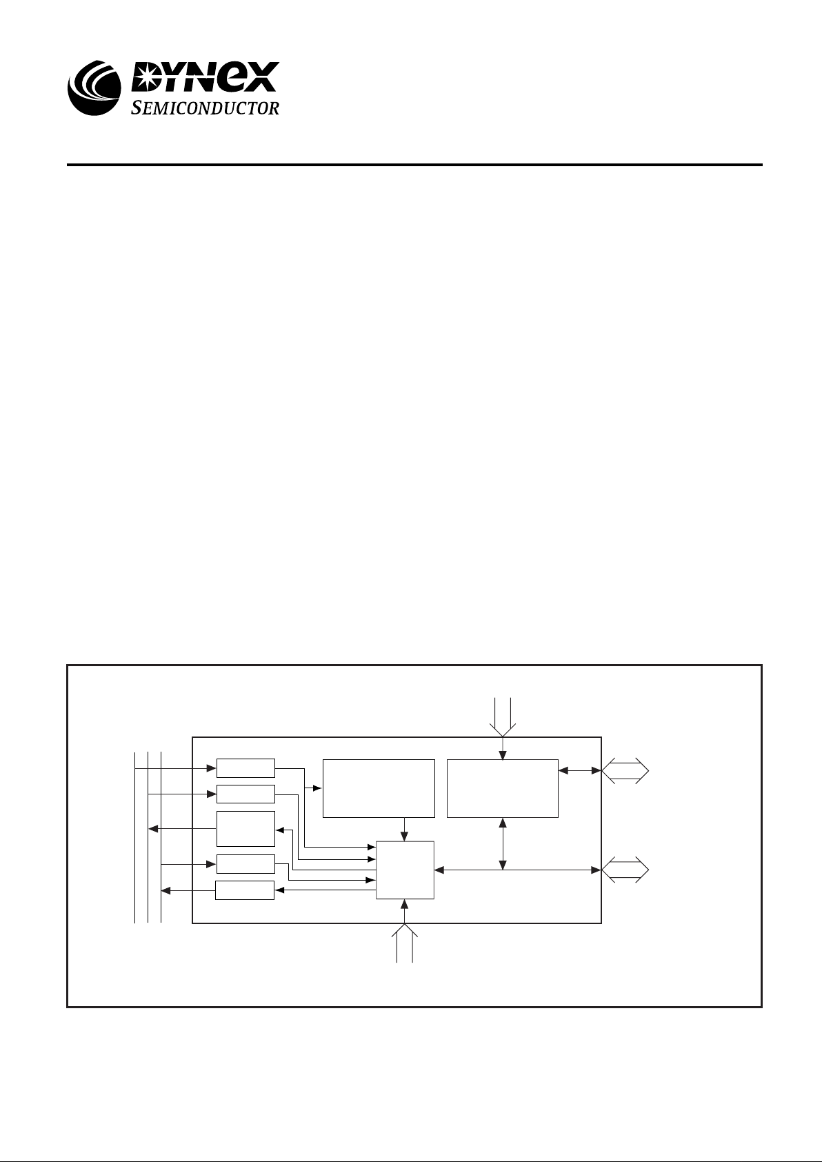
The OBT ASIC will interface any user to the ESA On Board
Data Handling bus. Developed under ESA Contract, it
conforms to ESA OBDH, Digital Bus Interface and Internal
User Bus Standards.
The OBT has 2 separate functions. The first is a 5 channel
modem which, on the bus side, provides the digital waveforms
necessary to operate the Litton Bus drivers, and receives the
outputs of the Litton bus detectors. On the user side, it
provides an input / output at Digital Bus Interface level. The
second function, internally coupled to the first, provides a
multiplexing / demultiplexing function of the DBI signals down
to Internal User Bus levels and vectored 16 bit serial register
read and write commands (see section 7.2 of ESA standard
TTC-B-01). In effect, the second function of the OBT provides
the core of an RTU.
The Interrogation and Response bus data streams of the
two functions may be either coupled together (in RT mode) or
isolated (in CT mode). The device may hence be used as a
modem only, an RTU kernel only or as a combined modem
and RTU kernel. In RT mode, the Interrogation bus data
stream can be observed and the Response bus data from
associated devices, such as an MA28138 Remote Bus
Interface, can be combined with that from the RTU kernel
before being used by the modem circuits to modulate the
Response bus. Bi-directional access to the Block Transfer bus
is provided in either mode.
When used to interface a central terminal to the OBDH bus,
the OBT should be continuously clocked in order to output
timing to all users on the I-bus as dummy interrogations from
the CT. Commands and telemetry are normally sent on the I
and BT busses whilst responses and telemetry normally return
on the R and BT busses.
Figure 1: Block Diagram
CONTROL
LOGIC
RTU
KERNEL
CONTROL
PINS
CLK DETECTOR,
WATCHDOG
DIGITAL
BUS
INTERFACE
INTERNAL
USER
BUS
CONFIGURATION PINS
OBDH BUS
I R BT
I Rx
R Rx
I (CTU)
R (RTU)
BT Rx
BT Rx
Tx
FEATURES
■ Radiation Hard
■ Low Power Consumption
■ Single CMOS-SOS ASIC Implementation
■ Latch-up Free
■ High SEU Immunity
■ Fully Compliant with ESA OBDH, IUB, DBI and RBI
Specification
■ Contains OBDH Bus Modem and RTU Kernel
■ Supports Bi-directional Data Transfer on Response and
Block Transfer Bus
MA28139
OBDH Bus Terminal
Replaces June 1999 version, DS3592-5.0 DS3592-6.0 January 2000
Page 2
MA28139
2/34
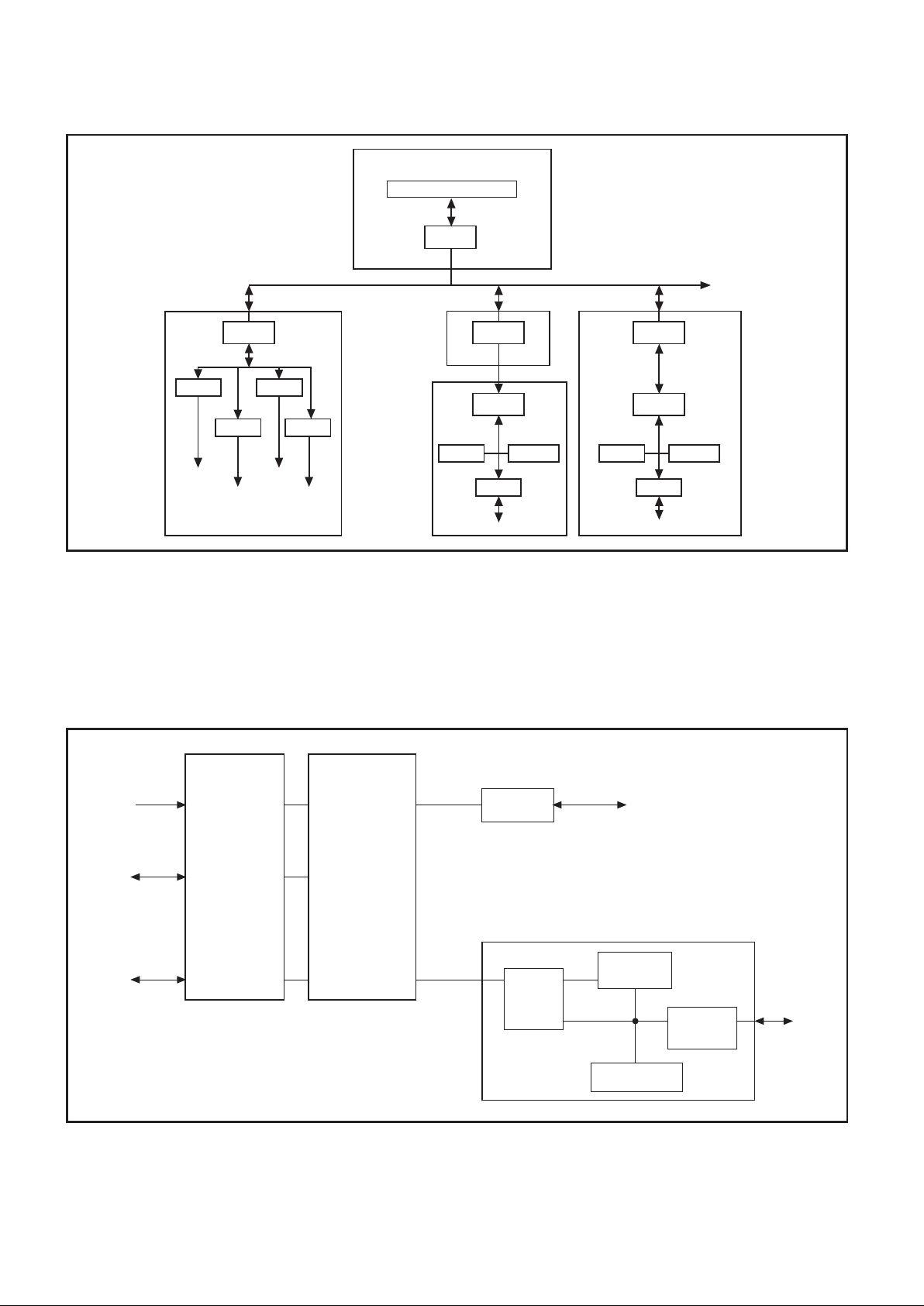
APPLICATION
PAYLOAD INTERFACES
The OBT converts the OBDH bus to an Internal User Bus,
and a Digital Bus Interface. The OBT can connect OBDH to
existing ESA standard payload interfaces such as the MSS
PIU (payload interface unit), ICU (intelligent control unit), SBC
Figure 3: Payload Interface
Figure 2: Application
DBI
IUB
PIU
PAYLOAD
BT-Bus
R-Bus
I-Bus
RBI
MA28138
µP
MEMORY
I/O
PAYLOAD
DMA
AD-BUS
SBC
OBDH
ANALOGUE
HYBRID
OR
DISCRETE
CIRCUIT
OBDH
BUS
TERMINAL
MA28139
(single board MIL-STD-1750 computer) or FTC (fault tolerant
computer).
The OBT and analogue components/transformers can be
integrated in the PIU, ICU, SBC, etc.
CENTRAL TERMINAL
Bus Controller
OBT
OBTOBTOBT
DMUX MPX
DMUX ADC
RBI
RAM µP
I/O
RBI
RAM µP
I/O
IUB
DBU
DBI
ODBH BUS
DBI
Commands
Timing
Digital
Data
Analogue
Data
Address
REMOTE TERMINAL
INTELLIGENT TERMINAL
DBI
CT
RT
RT
UP TO A T OTAL OF 62 TERMINALS
Page 3

MA28139
3/34
FUNCTIONAL DESCRIPTION
In RT mode, power up resets the OBT and causes it to
deselect both busses. Two watchdog counters monitor the
Nominal l-bus and the Redundant l-bus. If either bus becomes
active, that bus will be selected. If the selected bus stops, the
OBT watchdog times out and resets both the OBT and the
user. If both busses become active, the Nominal bus will be
selected in preference to the Redundant one. A change in bus
selection will always result in the OBT and the user being
reset. Responses from the user are always returned on the
selected bus. Setting ‘SIMUL’ high causes both BATs to drive
both the Nominal and the Redundant busses irrespective of
the current bus selection. The time-out period may be set to
any desired number of bits by varying the ‘LOSC’ frequency.
The OBT derives all timing from, and is synchronous with, the
selected l-bus. The OBT demodulates the l-bus to the DBI and
decodes commands to the IUB.
The CTpRTn mode pin causes the modem circuits and the
RTU Kernel to be either cascade or isolated. If CTpRTn is low
(RT mode), the RIRSYNC, CLK, DATA and VAL signals are
routed to the RTU Kernel and the associated pins act as
outputs; responses from the RTU Kernel are ORed with those
from the external RRTDATA and RRTEN inputs and can be
independently monitored on the DATARRT and ENRRT pins.
In this mode any reset caused by the Clock Detector
watchdogs is also combined with the power up reset input.
If CTpRTn is high (CT mode), the modem and RTU Kernel
functions are isolated to permit the device to be used as either
a modem within the CTU or an RTU Kernel interfacing to an
external modem where the RIRSYNC, CLK, DATA and VAL
pins act as inputs. The right-hand multiplexer bank is switched
to the upper position so that the CT drives the OBDH via the
CIT and CBT (if used) pins and receives responses/telemetry
via the CRR and CBR (if used) pins. Note: in CT mode, BAT1
must be connected to the l-busses.
In RT mode, the CITSEL, MOD, CLK, SYNC and INV pins
are disabled and the clocks are supplied by the l-bus BAR in
response to the selected bus. In CT mode, the Clock Detector
is functional and drives the TlMEOUTn pin but is unable to
cause internal reset on time-out; in this mode the CT must
supply all clocks and select the operational bus.
The changes depending upon selection of RT mode or CT mode with the CTpRTn pin are defined in the table below:
Functional Signal CT Mode Source RT Mode Source
(CTpRTn = ‘1’) (CTpRTn = ‘0’)
BAT1, 2 modulation clock CITMOD input pin Recovered R2F
BAT1, 2 data clock CITCLK input pin Recovered RIRCLK
BAT1 data input RRTDATA input pin RRTDATA OR DATARRT (RTU Kernel)
BAT1 tx enable ‘1’ RRTEN OR DATAEN (RTU Kernel)
BAT1 sync code tx enable CITSYNC input pin ‘0’
BAT1 bit invalidate tx enable CITINV input Pin ‘0’
BAT1, 2 bus selection CITSEL and SIMUL input pins Detected active bus and SIMUL input pin
BAT2 data input RBTDATA input Pin RBTDATA input pin
BAT2 tx enable RBTEN input pin RBTEN input pin
BAT1, 2, BAR1, 2, 3 reset MRSTn input pin TlMEOUTn AND MRSTn input pin
RIRSYNC, CLK, DATA, outputs inputs
VAL pin direction
BAT/BAR and RTU Kernel separated coupled
coupling
Page 4
MA28139
4/34
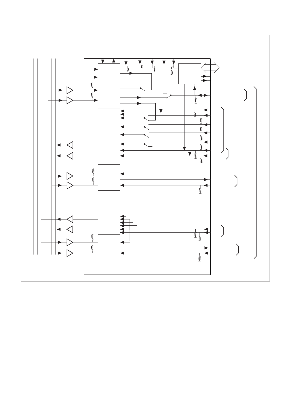
Figure 4: Architecture
MODEM Modulation Waveforms are compliant with ESA document THB/Apo/KZ/1386/av. Waveforms indicating the
operation of BAT1, 2 and BAR1, 2, 3 in both the CT and RT modes are shown in Figures 5 to 8.
Note: Switches in lower position - RT mode
Switches in upper position - CT mode
BUS
TIME
OUT SIMULCTMODE RESET
IUB
SYNC, CLK, DATA, VAL RIR
SEL
MOD
CLK
SYNC
INV
DATA
EN
CLK, DATA, VAL
INIT
DATA
EN
CLK, DATA, VAL
INIT
RBR/
CBR
RBT/CBT
RRR/CRR
CIT
RRT
DBI
BAR1
I-BUS RX
BAT1
BAR2
R-BUS RX
BAT2
BT-BUS TX
BAR3
BT-BUS RX
MA28139 OBT
0v
CLK
2F
OBDH
CLOCK
DETECTOR
WATCHDOG
NOMINAL
BUS #1
REDUNDANT
BUS #2
I R BT
I R BT
NIDS1/2n,
RIDS1/2n
RR1-4,
NRE, RRE
NRDS1/2n
RRDS1/2n
BR1-4,
NBE, RBE
NBDS1/2n,
RBDS1/2n
R-BUS TX
(RT MODE)
I-BUS TX
(CT MODE)
TA0-5
TAV
DATARRT
ENRRT
RTU
KERNEL
0v
BUS 1/2
ACTIVE
LOSC
OPEN
Page 5
MA28139
5/34
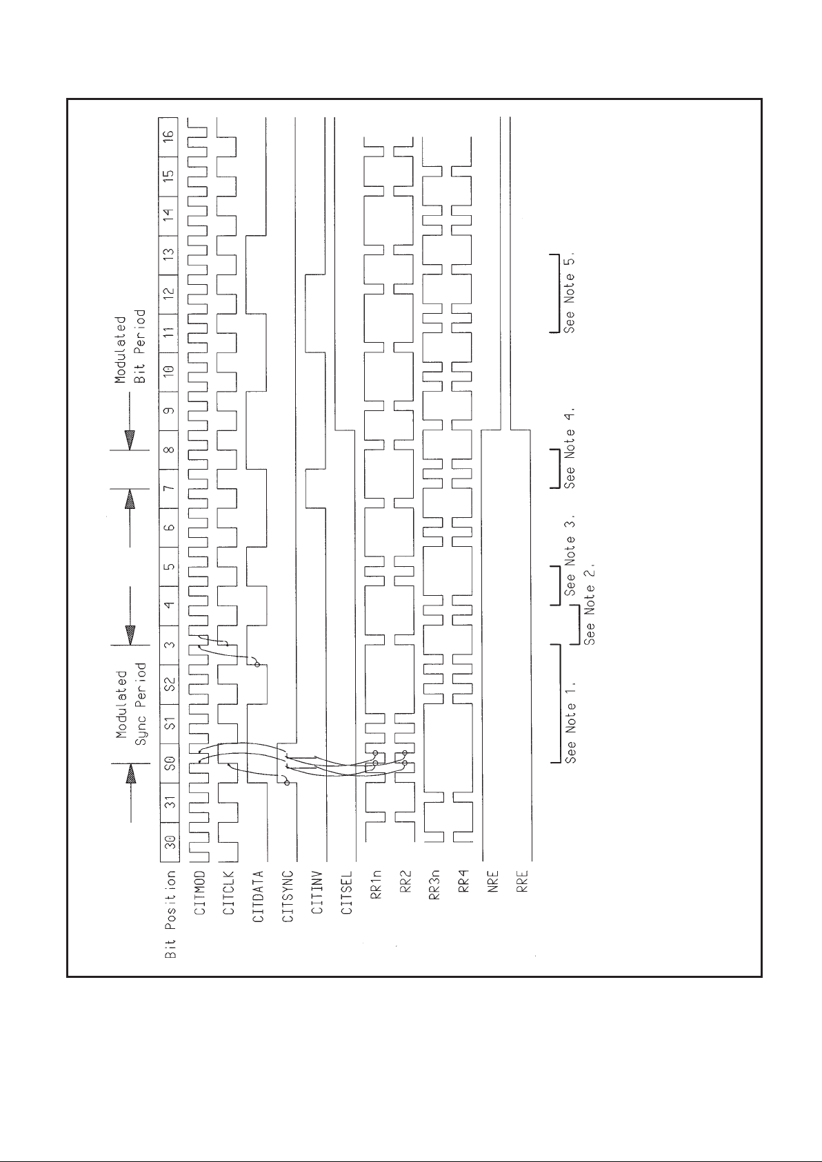
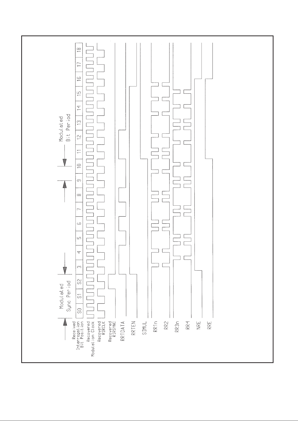
Figure 5: CT Mode Bus Adaptor Transmitter Waveforms
Note 1: Raising CITSYNC for one bit period causes an invalid bit, a valid bit and another invalid bit to be modulated. The exact pattern is determined
by RRTDATA; ‘110’ gives the classic H0H0H0L0L0L0 sync pattern.
Note 2: Valid Litton ‘1’ modulated.
Note 3: Valid Litton ‘0’ modulated.
Note 4: Invalid Litton ‘0’ modulation is caused by raising CITINV for one bit period.
Note 5: Raising CITINV for more than one bit period only causes one invalid bit to be modulated.
Note 6: BAT2 operation is similar, but SYNC and INV are not available.
Page 6
MA28139
6/34
Figure 6: RT Mode Bus Adaptor Transmitter Waveforms
Note: BAR2 and BAR3 operation are similar with different nomenclature.
Page 7
MA28139
7/34
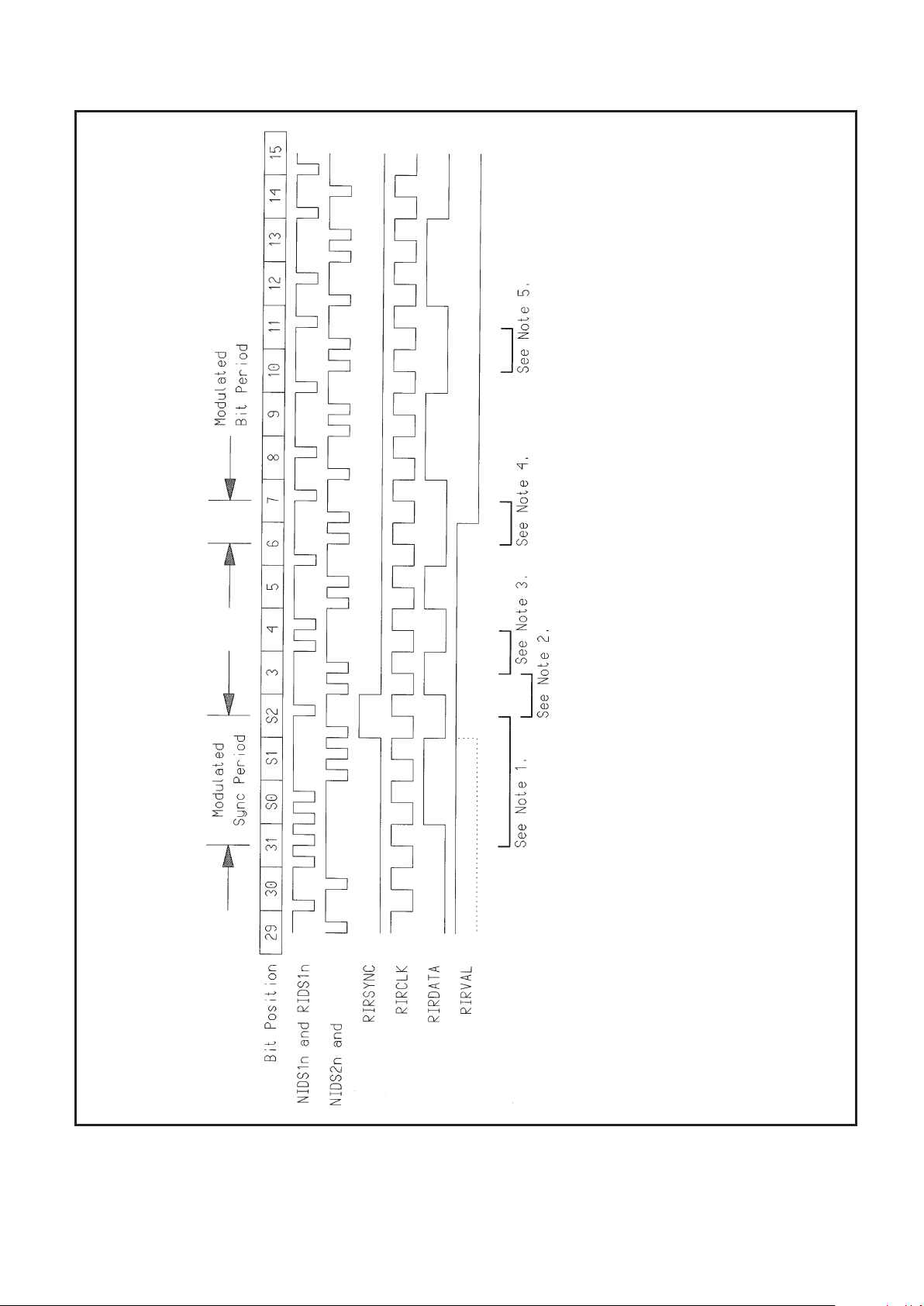
Figure 7: RT Mode Bus Adaptor Receiver Waveforms
Note 1: H0H0H0L0L0L0 sync pattern detected and resets phase of RIRCLK.
Note 2: Valid Litton ‘1’ detected.
Note 3: Valid Litton ‘0’ detected.
Note 4: Invalid Litton ‘0’ detected.
Note 5: Further invalid bits do not affect RIRVAL - it will rise as RIRSYNC rises.
Note 6: BAR2 and BAR3 operation is similar, but SYNC is not available and RRRINIT and RBRINIT are provided.
RIDS2n
Page 8
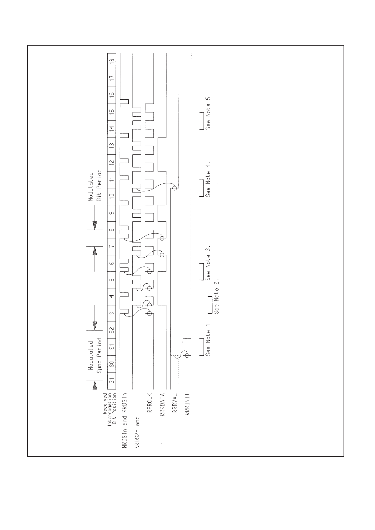
MA28139
8/34
Figure 8: BAR2 Bus Adaptor Receiver Waveforms
Note 1: RRRINIT asynchronously resets RRRVAL to clear errors detected in the previous response.
Note 2: Valid Litton ‘1’ detected.
Note 3: Valid Litton ‘0’ detected.
Note 4: Invalid Litton ‘0’ detected.
Note 5: Further invalid bits do not affect RRRVAL - it will rise as RRRINIT rises.
Note 6: BAR3 operation is similar, but is intended to support Block Transfer - RBRINIT hence occurs once per block.
Note 7: Operation of BAR2 and BAR3 does not depend on RT mode or CT mode, except for bus selection.
RIDS2n
Page 9
MA28139
9/34
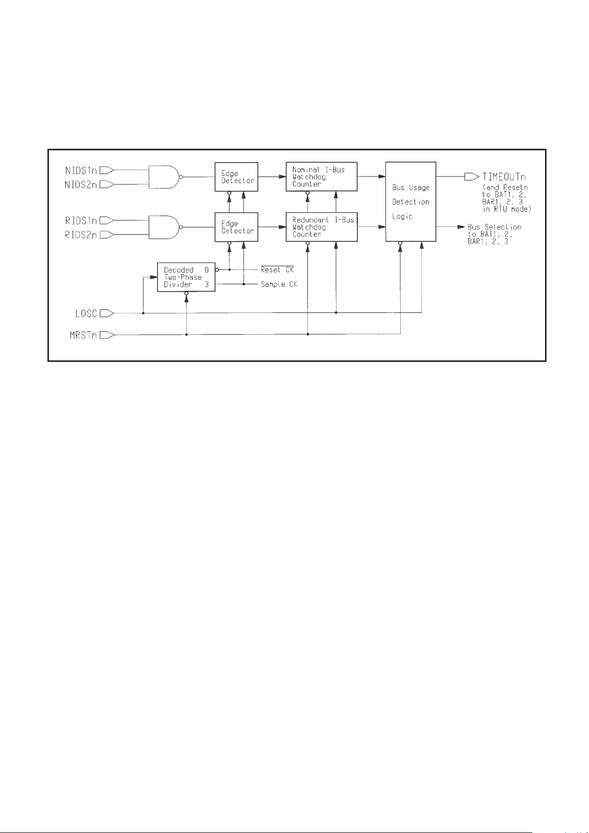
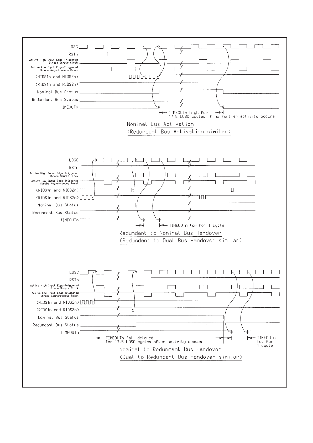
CLOCK DETECTOR OPERATION
The Clock Detector architecture is shown in Figure 9; a
separate channel is essentially provided for each of the
Nominal and Redundant Interrogation busses. Associated
waveforms are shown in Figure 10.
Figure 9: Clock Detector Architecture
Each channel contains an Edge Detector and a 5-bit
Watchdog Counter which respond only to high-to-low
transitions on their respective Interrogation bus DS1n inputs. A
common Bus Usage Detection circuit is used to generate timeout pulses (used for internal and external reset) and bus
selection signals from the results of the watchdogs.
The local oscillator input, LOSC, is divided and decoded to
generate an active low reset and an active high sample clock.
When applied to both input Edge Detectors, these signals
permit input high-to-low transitions to be detected for one
LOSC cycle in every two (between the reset ↓ and sample
clock ↑). Once such transitions have been detected by a
sample clock, the associated watchdog counter is reset. The
MSB of each watchdog counter is used as an indication of its
bus’s status - active or inactive. Should the watchdog counter
overflow (i.e. its MSB be set to 1), the associated bus will be
considered inactive.
The status of the Nominal and Redundant Interrogation
busses is used to determine internal bus selection for the
modulation of Response and Block Transfer data in the
device’s RT mode. If neither bus is considered active, the
TlMEOUTn pin will be held low and RT mode reception of all 3
busses will be inhibited. If one bus is considered active, RT
mode reception will occur on the same set of bus circuits
(redundancy) as the active Interrogation bus. If both busses
are considered active, RT mode reception from the Nominal
set of bus circuits will be performed. RT mode transmission will
always occur on the same set of bus circuits (redundancy) as
selected for reception unless the SIMUL pin is held high, in
which case transmission will occur simultaneously on both the
Nominal and Redundant busses.
Both watchdog counters are fully set at power up to mark
both busses as inactive - in this way, a missing LOSC input will
not cause inactive busses to be deemed active.
For a single detected input transition, 17.5 to 18.5 LOSC
cycles will elapse before the relevant bus is considered
inactive. If near-instantaneous Nominal-to-Redundant or Dualto-Redundant bus handover occurs, the change-over will be
delayed by 18 to 19 LOSC cycles, in order to preserve the
priority of the Nominal bus. If near-instantaneous Redundantto-Nominal or Redundant-to-Dual bus handover occurs, the
change-over will occur after 1.5 to 2.5 LOSC cycles since the
Nominal bus takes priority. In either of these cases, a 1 LOSC
cycle TlMEOUTn pulse is always generated to ensure that
internal reset occurs.
The frequency of the local oscillator may be varied to make
the nominal time-out period of 17.5 LOSC cycles correspond
to any desired number of (missing) bits on the Interrogation
bus. Variation of the duty cycle does not vary the time-out
period. After 16 LOSC cycles without detected input
transitions, the associated watchdog times-out and is detected
on the next LOSC ↑ edge; the generation of a TlMEOUTn
pulse and reset are then inevitable.
For proper Clock Detector operation, (at least) one high-tolow input transition must be detected within a period of 16
LOSC cycles of the last such detection, but transitions made
during alternate LOSC cycles (the phase is difficult to predict)
will not be detected. Local oscillator clock signals which are
harmonically-related to the modulation clock by an integer ratio
are thus a cause for concern, although this problem is perhaps
only likely to occur in experimental set-ups.
Page 10
MA28139
10/34
Figure 10: MA28139 Clock Detector Operation
Note: If both busses are determined by their watchdogs to be active (as indicated above by their status), the
Nominal Bus will always be used by the Bus Adaptor Transmitter and Receiver circuits instead of the
Redundant Bus.
Page 11

MA28139
11/34
The requirement to respect set-up and hold times for the
capture of the Edge Detector outputs by the LOSC high-to-low
transition means that LOSC signals which are harmonicallyrelated to the Litton modulation clock but whose phase can not
be controlled can never be guaranteed to provide reliable
operation.
For asynchronous local oscillator signals, there will be no
concern if we are simply able to place two or more Litton DSn
high-to-low edges into each LOSC cycle, so that:
τ
MOD
≤ τ
LOSC
- tSU - t
HOLD
and the time-out period of 16 τ
LOSC
is hence approximately
8 bit periods or more.
However, suppose that the periods of the modulation clock
and the local oscillator clock are such that the relationship
between them is:
τ
MOD
= m τ
LOSC
where m is a positive integer.
In order to respect the setup and hold times, tSU + t
HOLD
respectively, between the DSn ↓, and LOSC ↓ edges, it is
necessary to avoid such harmonic relationships; it can be
shown that around these spot frequencies it is necessary to
ensure that either:
w τ
MOD
≥ x τ
LOSC
+ tSU + t
HOLD
or
y τ
MOD
≤ z τ
LOSC
- tSU - t
HOLD
where the integer constants w, x, y and z are given in the
table below.
Since two modulation clock cycles occur per bit, the timeout period at these harmonics will then be:
16 τ
LOSC
≈ 16 τ
MOD
/ m ≈ 8 / m bit periods.
m w x y z Approx. time-out
period (bit periods)
1 151517178
27158154
3 5 15 5 15 2.67
43134152
5 3 15 3 15 1.6
6 2 13 2 11 1.33
717171.14
8192151
919190.88
10 1 11 1 9 0.8
11 1 11 1 11 0.73
12 1 13 1 11 0 67
13 1 13 1 13 0.62
14 1 15 1 13 0.57
15 1 15 1 15 0.53
In summary, slow local oscillator clocks which cause
relatively long timeout periods ≥ 8 bit periods are not
considered a problem; very long time-outs can be reliably
implemented. For shorter time-out periods, however, it is
necessary to avoid harmonic relationships between the Litton
modulation clock and the local oscillator. The simplest
practical method for avoiding such relationships would be to
arrange for the ratio
n = τ
MOD
/ τ
LOSC
to have a half-integer value such that n = 0.5, 1.5, 2.5,
...using an independent crystal oscillator if necessary.
Page 12

MA28139
12/34
OBDH / IUB INTERFACE
The Central Terminal Unit controls timing, commands and
telemetry to all subsystems on the OBDH bus. ESA TTC-B-01
specifies the OBDH to be 2 redundant sets (Nominal and
Redundant) of 2 twisted pairs (Interrogation and Response
bus) plus an optional redundant 3rd twisted pair (Block
Transfer bus), Litton modulated (self clocking with parity on
each bit), balanced transformer coupled for less than 1 error in
100 million bits on a 25 metre bus. The data rate is nominally
500K Bits/sec although the chip itself supports up to 5MBits/
sec. The OBT is transformer coupled with adjustable reference
and threshold levels as shown below. Litton more positive than
V
th+
makes discriminator signal NIDS1n low. Litton more
negative than V
th-
makes NIDS2n low. OBT RR1n, RR2,
RR3n, RR4 control 4 switches which drive the bus with bipolar
Litton code when enabled. For clarity redundancy is not shown
below:
TTC-B-01 also specifies the IUB. The OBT supplies
specified clocks, memory load address for ML data (or channel
address for mode command) and responds on the R bus with a
13 zeroes response as acknowledgement. If the command
requires data aquisition, the OBT responds with a 13 or 21 bit
response containing 8 or 16 bits (respectively) of user data,
controlling external ADC as required.
Note: Connections
to redundant OBDH
busses omitted for
clarity.
Figure 11: OBDH to IUB interface
+5V
I-BUS
OBT
+
-
+
-
CLOCKS
ML ADDRESS
ML DATA
CHANNEL ADDRESS
MODE COMMAND
ANALOG TO DIGITAL
CONVERTER CONTROLS
IUB
ENABLE
GND
+5V
GND
REF
R-BUS
DATA
V
th+
V
th-
NIDS1n
NIDS2n
RR1n
RR3n
RR2
RR4
Page 13

MA28139
13/34
RTU KERNEL PROTOCOL VIOLATIONS
Some commands to the RTU Kernel cannot be completed
within one Interrogation period (or “slot”) because of the need
to provide a slow external interface as defined in ESA standard
TTC-B-01. These are commands for 16-bit Digital Serial
Acquisition (S16) and 16-bit Memory Load (ML). In addition, it
is also possible to inhibit On/Off commands by pin
configuration.
Consequently:
■ a Memory Load command cannot be followed by another
Memory Load command in the next Interrogation; the
second command of such a sequence will be ignored,
■ a 16-bit Digital Serial Acquisition (S16) cannot be
followed by another acquisition or command in the next
Interrogation; the second command of such a sequence
will be ignored,
■ a Long On/Off command will be ignored if the On/Off
command Inhibit input pin, OOINH, is high.
RTU KERNEL MODE DEFINITIONS
The mode field contained in bits 19 to 22 of the
Interrogation is decoded during acquisition commands to drive
one of the MOSC, MOLC, MOHL, MOBT, MODBL, MODS8,
MODS16, MOANS or MOAND outputs. Mode decoding is an
extension of that defined in ESA standard TTC-B-01 Table 7.1
and is shown in Table 1 below:
Note that in all MODE Dependent Command and
Acquisition Interrogations, bits 23 to 30 of the Interrogation are
output as an 8 bit channel address on CHADD(0:7). ESA
standard TTC-B-01, p.110 specifies a 7 bit channel address in
bits 27 to 29, leaving bit 30 as Reserved. For complete
compliance with this standard, CHADD(7) should be
disregarded and CHADD(0:6) only should be used.
The signals generated by the RTU Kernel during 8-bit
Single-Ended and 8-bit Double-Ended Analog Data
Acquisitions are intended for connection to an 8-bit serial ADC
module. The outputs PC, ANCLK, SOC and SH are intended
to provide ADC power control, conversion clock, start of
conversion pulse and sample/hold control respectively.
RTU Kernel BroadCast Pulse and BCP Validity Waveforms
are shown in Figure 12.
RTU Kernel Memory Load Command Waveforms are
shown in Figure 13.
RTU Kernel MODE Dependent Command and Acquisition
Waveforms are shown in Figures 14 - 17.
Mode Code Associated
Bit 19 Bit 20 Bit 21 Bit 22 Function Output Pin
0 0 0 0 Unused 0 0 0 1 Short Switch Closure On/Off Command MOSC
0 0 1 0 Long Switch Closure On/Off Command MOLC
0 0 1 1 High Power Switch Closure On/Off Cmd MOHL
0 1 0 0 Unused 0 1 0 1 Unused 0 1 1 0 Unused 0 1 1 1 Block Transfer Command MOBT
1 0 0 0 8-bit Digital Bi-Level Data Acquisition MODBL
1 0 0 1 Unused 1 0 1 0 16-bit Serial Digital Data Acquisition MODS16
1 0 1 1 8-bit Serial Digital Data Acquisition MODS8
1 1 0 0 8-bit Single-Ended Analog Data Acquisition MOANS
1 1 0 1 Unused 1 1 1 0 8-bit Double-Ended Analog Data Acquisition MOAND
1 1 1 1 Unused -
Table 1: RTU Kernel Mode Definitions
Page 14

MA28139
14/34
Figure 12: BroadCast Pulse and BCP Validity Waveforms
Bit Position
RIRSYNC
RIRCLK
RIRDATA
RIRVAL
BCP(1:4)
BCPVAL
Note 1: Bit 6 of the Interrogation will be interpreted as BCP(4) if (EXTFMT = 0);
if (EXTFMT = 1), the BCP (4) output will be 0 and bit 6 will be interpreted as TA(0).
Note 2: (RIRVAL = 0) (presumably because of bad Interrogation length or received Litton coding errors detected by the
modem), bad received parity in bit 31 of the Interrogation or wrong Interrogation length will both cause the
Interrogation to be rejected and will set BCPVAL = 0.
Bit Position
RIRSYNC
RIRCLK
RIRDATA
RIRVAL
BCP(1:4)
BCPVAL
= BCP(4) or TA(0)
1
1
Page 15

MA28139
15/34
Bit Position
RIRSYNC
RIRCLK
RIRDATA
RIRVAL
IRCLK
TRCLK
CTCLK
MLADD(0:4)
MLDATA
DATARRT
ENRRT
Bit Position
RIRSYNC
RIRCLK
RIRDATA
RIRVAL
IRCLK
TRCLK
CTCLK
MLADD(0:4)
MLDATA
DATARRT
ENRRT
Figure 13: Memory Load Command Waveforms
Note 1: One Memory Load command takes 2 Interrogations to complete. Consecutive Memory Load commands are hence not
possible and form a protocol violation. The second Memory Load command of such a sequence will be rejected.
Note 2: For a Memory Load command to be decoded, the evaluated Memory Load Address must be non-zero. An evaluated
Memory Load Address of zero implies data aquisition.
Note 3: The Memory Load Address which is evaluated for decoding and addressing usage may vary from 3 to 5 bits.
If (EXTMLA1 = 1) and (EXTMLA2 = 0), the Memory Load Address field is extended to 4 bits and bit 11of the
Interrogation will be treated as MLA(1).
If (EXTMLA2 = 1), the Memory Load Address field is extended to 5 bits and bits 10 and 11of the Interrogation will be
treated as MLA(0:1).
Any Interrogation bits treated as Extended Memory Load Address bits will not be treated as Terminal Address bits; this
facility is intended for 2x or 4x size expansion provided that up to 4 consecutive Terminal Addresses can be used.
Note 4: The Memory Load command response is always 13-zeros.
= BCP(4) or TA(0)
= TA(4:5) or MLA(0:1)
1
2
1
2
Page 16

MA28139
16/34
Figure 14: 8-Bit Digital Serial and 8-Bit Digital Bi-Level Acquisition Waveforms
Note 1: For any acquisition command to be decoded, the evaluated Memory Load Address must be zero. An evaluated Memory Load
Address of non-zero does not imply data acquisition.
Note 2: The Memory Load Address which is evaluated for decoding and addressing usage may vary from 3 to 5 bits.
If (EXTMLA1 = 1) and (EXTMLA2 = 0), the Memory Load Address field is extended to 4 bits and bit 11 of the Interrogation will be
treated as MLA(1).
If (EXTMLA2 = 1), the Memory Load Address field is extended to 5 bits and bits 10 and 11of the Interrogation will be
treated as MLA(0:1).
Any Interrogation bits treated as Extended Memory Load Address bits will not be treated as Terminal Address bits; this facility is
intended for 2x or 4x size expansion provided that up to 4 consecutive Terminal Addresses can be used.
Note 3: The 8-bit Digital Serial and 8-bit Digital Bi-Level Acquisition command responses are always 13 bits in length; the Destination
Address is simply copied from the Interrogation into the Response.
Bit Position
RIRSYNC
RIRCLK
RIRDATA
RIRVAL
IRCLK
TRCLK
CTCLK
CHADD(0:7)
MODS8 or
DIGIN
DATARRT
ENRRT
MODBL
Bit Position
RIRSYNC
RIRCLK
RIRDATA
RIRVAL
IRCLK
TRCLK
CTCLK
CHADD(0:7)
MODS8 or
DIGIN
DATARRT
ENRRT
MODBL
Page 17

MA28139
17/34
Figure 15: 16-Bit Digital Serial Acquisition Waveforms
Bit Position
RIRSYNC
RIRCLK
RIRDATA
RIRVAL
IRCLK
TRCLK
CTCLK
CHADD(0:7)
MODS16
DIGIN
DATARRT
ENRRT
Bit Position
RIRSYNC
RIRCLK
RIRDATA
RIRVAL
IRCLK
TRCLK
CTCLK
CHADD(0:7)
MODS16
DIGIN
DATARRT
ENRRT
Note 1: One 16-bit Digital Serial Acquisition command takes 2 Interrogations to complete. A succeeding Acquisition or Switch
Closure command of any type is hence not possible and forms a protocol violation. The second command of such a sequence
will be rejected.
Note 2: For any acquisition command to be decoded, the evaluated Memory Load Address must be zero. An evaluated Memory Load
Address of non-zero does not imply data acquisition.
Note 3: The Memory Load Address which is evaluated for decoding and addressing usage may vary from 3 to 5 bits.
If (EXTMLA1 = 1) and (EXTMLA2 = 0), the Memory Load Address field is extended to 4 bits and bit 11 of the Interrogation will be
treated as MLA(1).
If (EXTMLA2 = 1), the Memory Load Address field is extended to 5 bits and bits 10 and 11 of the Interrogation will be
treated as MLA(0:1).
Any Interrogation bits treated as Extended Memory Load Address bits will not be treated as Terminal Address bits; this facility is
intended for 2x or 4x size expansion provided that up to 4 consecutive Terminal Addresses can be used.
Note 4: The 16-bit Digital Serial Acquisition command response is always 21 bits in length; the Destination Address is simply
copied from the Interrogation into the Response.
Page 18

MA28139
18/34
Bit Position
RIRSYNC
RIRCLK
RIRDATA
RIRVAL
IRCLK
TRCLK
CTCLK
CHADD(0:7)
MOANS
PC
ANCLK
SOC
SH
ANSIN
DATARRT
FNRRT
or MOAND
Note 1: For any acquisition command to be decoded, the evaluated Memory Load Address must be zero. An evaluated
Memory Load Address of non-zero does not imply data acquisition.
Note 2: The Memory Load Address which is evaluated for decoding and addressing usage may vary from 3 to 5 bits.
If (EXTMLA1 = 1) and (EXTMLA2 = 0), the Memory Load Address field is extended to 4 bits and bit 11 of the
Interrogation will be treated as MLA(1).
If (EXTMLA2 = 1), the Memory Load Address field is extended to 5 bits and bits 10 and 11of the Interrogation will
be treated as MLA(0:1).
Any Interrogation bits treated as Extended Memory Load Address bits will not be treated as Terminal Address
bits; this facility is intended for 2x or 4x size expansion provided that up to 4 consecutive Terminal Addresses can
be used.
Note 3: The 8-bit Analog Single-Ended and 8-bit Analog Double-Ended Acquisition command responses are always 13
bits in length; the Destination Address is simply copied from the Interrogation into the Response.
Figure 16: 8-Bit Analog Single-Ended and 8-Bit Analog Double-Ended (Serial) Acquisition Waveforms
Page 19

MA28139
19/34
Bit Position
RIRSYNC
RIRCLK
RIRDATA
RIRVAL
IRCLK
TRCLK
CTCLK
CHADD(0:7)
MOANS
PC
ANCLK
SOC
SH
ANSIN
DATARRT
FNRRT
or MOAND
Figure 16 continued
Page 20

MA28139
20/34
Figure 17: Short-Command, Long-Command and High-Level Switch Closure and Block Transfer Command Waveforms
Bit Position
RIRSYNC
RIRCLK
RIRDATA
RIRVAL
IRCLK
TRCLK
CTCLK
CHADD(0:7)
DATARRT
ENRRT
MOSC, MOLC,
MOHL or MOBT
Bit Position
RIRSYNC
RIRCLK
RIRDATA
RIRVAL
IRCLK
TRCLK
CTCLK
CHADD(0:7)
DATARRT
ENRRT
MOSC, MOLC,
MOHL or MOBT
Note 1: The Block Transfer command does not require a Channel Address; CHADD(0:7) is set therefore to zero.
Note 2: For any acquisition command to be decoded, the evaluated Memory Load Address must be zero. An evaluated Memory Load
Address of non-zero does not imply data acquisition.
Note 3: The Memory Load Address which is evaluated for decoding and addressing usage may vary from 3 to 5 bits.
If (EXTMLA1 = 1) and (EXTMLA2 = 0), the Memory Load Address field is extended to 4 bits and bit 11 of the Interrogation will be
treated as MLA(1).
If (EXTMLA2 = 1), the Memory Load Address field is extended to 5 bits and bits 10 and 11of the Interrogation will be
treated as MLA(0:1).
Any Interrogation bits treated as Extended Memory Load Address bits will not be treated as Terminal Address bits; this facility is
intended for 2x or 4x size expansion provided that up to 4 consecutive Terminal Addresses can be used.
Note 4: The Short-Command, Long-Command, High-Level Switch Closure and Block Transfer command responses are always 13-zeroes.
Page 21

MA28139
21/34
THE ESA ON-BOARD DATA HANDLING
(OBDH) BUS
The dual redundant OBDH bus is connected to the OBT
bus interface via an input descriminator and an output bridge
driver circuit. These convert between the bipolar LITTON code
and the standard CMOS inputs and outputs of the IC.
The OBDH bus is divided into three parts:
A. INTERROGATION BUS (I BUS)
This bus is used to transfer data from the CT to the
RTs, as commands of 32 bit words, each bit being modulated
according to the Litton scheme shown in Figure 18. Each
Interrogation (or command) “slot” comprises 3 Sync bits, 3 or 4
BroadCast Pulses, 5 or 6 Terminal Address bits, 4 Destination
Address bits, 16 Data bits and a Parity bit.
B. RESPONSE BUS (R BUS)
This bus is used to send data from the RTs to the CT, (can
be used by RTs to receive data). Each response word
comprises the 4 Destination Address bits sent in the
corresponding Interrogation, either 8 or 16 Data bits from the
user (8 bits unless a 16 bit acquisition was requested and 8
zeros if no response data is required) and a single Stop bit
(used to ensure data is fully clocked through bus modems and
0 by convention).
C. BLOCK TRANSFER BUS (BT BUS)
Used to transfer blocks of data between the CT and RTs, in
either direction, as a contiguous block or stream of data bits.
Figure 18: Litton Coded Data
logical
"1"
logical
"0"
invalid
logic
"1"
invalid
logic
"0"
high -
low -
0v -
high -
0v -
high -
low -
0v -
low -
0v -
invalid
logic
"1"
high -
0v -
logical
"1"
invalid
logic
"0"
low -
Synchronisation Pattern
FASTER OBDH/DBI COMPATIBLE NETWORKS
With analog components the OBT can interface any
equipment to the specified ESA OBDH bus at the nominal data
rate of 0.5 Mbps. Contract 5352 proved that analog
components limit OBDH data rate to 2 Mbps maximum. But
OBTs work to over 5 Mbps (10MHz with 2 clocks/bit Litton
coded). OBTs may be directly networked via digital bus
drivers/receivers, (eliminating analog components) using
Litton coded 4 wire (R2/DS1 and R4/DS2) busses (see OBDH
application note 1). MSS made a 3 metre optical OBDH
network for the Pegasus ion source.
DBIs may be directly connected but will not be Litton coded
with Parity on every bit, or exhibit modulation and
demodulation delays.
Page 22

MA28139
22/34
CONNECTIONS TO THE OBDH I, R AND BT BUSSES (SUGGESTED SCHEMES ONLY)
TRANSMITTER
Two OBDH bus driver schemes based on complementary and N-channel enhancement-mode FETs are shown.
Current-limiting and protection resistors may be employed to prevent damage under short-circuit.
Latching and/or non-latching relays may be used to provide isolation from the bus when a redundant circuit is unused or unpowered.
NPN and/or PNP bipolar junction transistors may also be employed in place of FETs.
Redundancy can be handled in channels (as shown) or by applying cross-strapping between the transformers and the drivers.
This implementation generates ‘active ground’ pulses where the transformer is shorted out (by conduction of the two lower FETs)
while the bus driver is enabled to reduce ringing, bus echoes, etc.
Using XR2 in place of XR3n and XR4 in place of XR1n will not cause ‘active zeros’ to be driven.
XR4
XR2
XR3n
XR1n
XR4
XR2
XR3n
XR1n
Figure 19: Conceptual OBDH Bus Driver Scheme
Page 23

MA28139
23/34
Figure 20: Conceptual OBDH Bus Window Discriminator Scheme
RECEIVER
Two OBDH bus window discriminator schemes, based on balanced and unbalanced techniques are shown.
Current-limiting and protection resistors may be employed to prevent damage under short-circuit.
Latching and/or non-latching relays may be used to provide isolation from the bus when a redundant circuit is unused or
unpowered.
Noise filtering and the effects of bus loading should be considered.
Redundancy can be handled in channels (as shown) or by applying cross-strapping between the transformers and the receivers.
Page 24

MA28139
24/34
DC CHARACTERISTICS AND RATINGS
Parameter Min Max Units
Supply Voltage -0.5 7 V
Input Voltage -0.3 VDD+0.3 V
Current Through Any Pin -20 +20 mA
Operating Temperature -55 +125 °C
Storage Temperature -65 +150 °C
Note: Stresses above those listed may cause permanent
damage to the device. This is a stress rating only and
functional operation of the device at these conditions, or at
any other condition above those indicated in the operations
section of this specification, is not implied. Exposure to
absolute maximum rating conditions for extended periods
may affect device reliability.
Table 2: Absolute Maximum Ratings
Parameter
Supply Voltage
CMOS input high voltage
CMOS input low voltage
Output high voltage
Output high voltage
Input Pull-down current
Input Pull-down current
Input Pull-up current
Input Pull-up current
Input leakage current
Output leakage current
Output leakage current
Static Power supply Current
Dynamic Power supply Current
Conditions
-
-
IOH = -1.0mA
IOL = 4.0mA
VDD = 5.5V, VIN = V
SS
VDD = 5.5V, VIN = V
DD
VDD = 5.5V, VIN = V
SS
VDD = 5.5V, VIN = V
DD
VDD = 5.5V, VIN = VSS or V
DD
VDD = 5.5V, V
OUT
= V
SS
VDD = 5.5V, V
OUT
= V
DD
VDD = 5.5V
f = 1MHz, VDD = 5.5V
Typ.
5.0
-
-
-
-
-
-
-
-
-
-
-
0.02
6
Symbol
V
DD
V
IH
V
IL
V
OH
V
OL
I
PDL
I
PDH
I
PUL
I
PUH
I
L
I
OZL
I
OZH
I
DD1
I
DD2
Min.
4.5
0.8V
DD
V
SS
VDD - 0.5
-
-25
25
-400
-25
-10
-30
25
-
-
Units
V
V
V
V
V
µA
µA
µA
µA
µA
µA
µA
mA
mA
Max.
5.5
V
DD
0.2 V
DD
-
0.4
25
400
-25
25
10
30
400
8
20
Notes: 1. VDD = 5V ±10% over full temperature range.
2. Total dose radiation not exceeding 105 Rads(Si).
3. Mil-Std-883, method 5005, subgroups 1, 2, 3.
4. All outputs are suitable for TTL/CMOS drive.
5. Electro-Static Discharge protection is provided for all pins.
6. Internal pull-up or pull-down resistors should not be relied upon for proper operation and/or termination of input levels
under all operating conditions without prior consultation with GPS.
7. Input and output leakage measurements are guaranteed but not tested at -55°C.
Table 3: DC Characteristics
Page 25

MA28139
25/34
AC CHARACTERISICS
No. Parameter Condition Min. Max. Units
T1 CITMOD to RR1n, RR2, RR3n, RR4, BR1n, CTU mode - 45 ns
BR2, BR3n, BR4
T2 CITMOD to NRE, RRE, NBE, RBE CTU mode - 55 ns
T3/ CITSYNC, CITINV to CITCLK ↑ (setup/hold) CTU mode 10 - ns
T3a
T4/4a RRTDATA to CITMOD ↓ (setup/hold) CTU mode 10 - ns
T5/5a RBTDATA to CITMOD ↓ (setup/hold) CTU mode 10 - ns
T6/6a RBTEN to CITMOD ↑ (setup/hold) CTU mode 10 - ns
T7/7a CITCLK to CITMOD ↑ (setup/hold) CTU mode 10 - ns
T8 NIDS1n, NIDS2n, RIDS1n, RIDS2n to RR1n RTU mode - 55 ns
RR2, RR3n, RR4, BR1n, BR2, BR3n, BR4
T9 NIDS1n, NIDS2n, RIDS1n, RIDS2n to NRE RTU mode - 75 ns
RRE, NBE, RBE
T10/ RRTDATA to NIDS1n, NIDS2n, RIDS1n, RTU mode 10 - ns
T10a RIDS2n ↓ (setup/hold)
T11/ RBTDATA to NIDS1n, NIDS2n, RIDS1n, RTU mode 10 - ns
T11a RIDS2n ↓ (setup/hold)
T12
RRTEN to NIDS1n, NIDS2n, RIDS1n, RIDS2n ↑ setup
RTU mode 0 - ns
T12a
RRTEN to NIDS1n, NIDS2n, RIDS1n, RIDS2n ↑ hold
RTU mode 35 - ns
T13
RBTEN to NIDS1n, NIDS2n, RIDS1n, RIDS2n ↑ setup
RTU mode 0 - ns
T13a
RBTEN to NIDS1n, NIDS2n, RIDS1n, RIDS2n ↑ hold
RTU mode 35 - ns
Table 4: Bus Adaptor Transmitter Characterisation
No. Parameter Condition Min. Max. Units
T14 NIDS1n, NIDS2n, RIDS1n, RIDS2n ↓ to RTU mode - 80 ns
RIRSYNC, RIRCLK, RIRDATA, RIRVAL valid
T15 NRDS1n, NRDS2n, RRDS1n, RRDS2n ↓ to RTU mode - 55 ns
RRRCLK, RRRDATA valid
T16 NBDS1n, NBDS2n, RBDS1n, RBDS2n to RTU mode - 55 ns
RBRCLK, RBRDATA valid
T17 NRDS1n, NRDS2n, RRDS1n, RRDS2n ↓ to RTU mode - 55 ns
RRRVAL ↓
T18 NBDS1n, NBDS2n, RBDS1n, RBDS2n to RTU mode - 55 ns
RBRVAL ↓
T19 RRRINIT to RRRVAL ↑ RTU mode - 30 ns
T20 RBRINIT to RBRVAL ↑ RTU mode - 30 ns
T21 NIDS1n, NIDS2n, RIDS1n, RIDS2n pulse RTU mode 12 - ns
width low (min.)
T22 NRDS1n, NRDS2n, RRDS1n, RRDS2n pulse RTU mode 12 - ns
width low (min.)
T23 NBDS1n, NBDS2n, RBDS1n, RBDS2n pulse RTU mode 12 - ns
width low (min.)
Table 5: Bus Adaptor Receiver Characterisation
Page 26

MA28139
26/34
No. Parameter Condition Min. Max. Units
T24 LOSC ↓ to NIDS1n, NIDS2n, RIDS1n, CTU mode or RTU mode 10 - ns
RIDS2n ↓ (hold max.)
T25 LOSC ↓ to NIDS1n, NIDS2n, RIDS1n, CTU mode or RTU mode 15 - ns
RIDS2n ↓ (setup max.)
T26 LOSC ↑↓ to TIMEOUTn valid CTU mode or RTU mode - 55 ns
Timeout period = 16τ
LOSC
CTU mode or RTU mode Guaranteed, not measured
Redundant to Dual or Redundant to Nominal CTU mode or RTU mode Guaranteed, not measured
bus changeover TIMEOUTn low reset period
= τ
LOSC
Table 6: Clock Detector Characterisation
No. Parameter Condition Min. Max. Units
T27 RIRCLK ↓ to BCP(1:4), BCPVAL valid CTU mode - 70 ns
T28 RIRCLK ↓ to MLADD(0:4) CTU mode - 80 ns
T29 RIRCLK ↓ to MLDATA CTU mode - 80 ns
T30 RIRCLK ↓ to CHADD CTU mode - 75 ns
T31 RIRCLK ↓ to MOSC, MOLC, MOHL, MOBT, CTU mode
MODBL, MODS16, MODS8, MOANS, - 70 ns
MOAND valid
T32 RIRCLK ↓ to IRCLK, CTCLK, TRCLK valid CTU mode - 70 ns
T33 RIRCLK ↓ to PC, ANCLK, SOC, SH valid CTU mode - 70 ns
T34 RIRCLK ↓ to DATARRT, ENRRT valid CTU mode - 55 ns
T35 ANSIN to RIRCLK ↑ setup RTU mode 0 - ms
T35a ANSIN to RIRCLK ↑ hold RTU mode 30 - ns
T36 NIDS1n, NIDS2n, RIDS1n, RIDS2n ↓ to RTU mode - 75 ns
DATARRT, ENRRT
Note 1: RTU mode timing parameters not explicitly stated will be lower than the sum of the appropriate parameters for the
RTU Kernel, BAR1 and BAT2. Parameters T34 and T36 above may be used to estimate the difference in timing
between CTU mode (i.e. where the RTU Kernel, BAR1 and BAT2 are not coupled together) and RTU mode usage
(i.e. where those components are coupled together).
Note 2: Configuration pins such as TA(0:5), EXTFMT, EXTMLA1 and EXTMLA2 and MRSTn are not considered here
because they do not need to be dynamically changed.
Note 3: V
DD
= 5V ±10% over full temperature range. VOH = VOL = VDD/2, VIL = VSS, VIH = VDD, CL = 50pF.
Note 4: Total dose radiation not exceeding 105 Rads (Si).
Note 5: Tables 4, 5, 6 & 7 contain Mil-Std-883, method 5005, subgroups 9, 10, 11.
Table 7: RTU Kernel Characterisation
Conditions
V
I
= 0V
V
I/O
= 0V
Min.
-
-
Typ.
3
5
Max.
5
7
Note 1: TA = 25˚C and f = 1MHz. Data obtained by characterisation or analysis; not routinely measured.
Table 8: Capacitance
Units
pF
pF
Parameter
Input Capacitance
Output Capacitance
Symbol
C
IN
C
OUT
Page 27

MA28139
27/34
Conditions
VDD = 4.5 - 5.5V, FREQ = 1 MHz
VIL = VSS, VIH = VDD, VOL = VOH = VDD/2
TEMP = -55˚C to +125˚C, GPS Pattern Set
Mil-Std-883, method 5005, subgroups 7, 8A, 8B
Table 9: Functionality
Symbol
F
T
Parameter
Functionality
Subgroup
1
2
3
7
8A
8B
9
10
11
Table 10: Definition of Subgroups
Definition
Static characteristics specified in Table 3 at +25˚C
Static characteristics specified in Table 3 at +125˚C
Static characteristics specified in Table 3 at -55˚C
Functional characteristics specified in Table 9 at +25˚C
Functional characteristics specified in Table 9 at +125˚C
Functional characteristics specified in Table 9 at -55˚C
Switching characteristics specified in Tables 4 to 7 at +25˚C
Switching characteristics specified in Tables 4 to 7 at +125˚C
Switching characteristics specified in Tables 4 to 7 at -55˚C
Page 28

MA28139
28/34
Figure 21: OBT Schematic
OBT
MLDATA
MLADD (0:4)
IRCLK
CTCLK
TRCLK
CHADD (0:7)
MOSC
MOLC
MOHL
MOBT
MODBL
MODS16
MODS8
MOANS
MOAND
PC
ANCLK
SOC
SH
DIGIN
ANSIN
TAV
BCP (1:4)
BCP VAL
ENRRT
DATARRT
OOINH
EXTMLA2
EXTMLA1
EXTFMT
TA (0:5)
DATA TO USER
CLOCKS TO USER
MODE ADDRESS TO USER
IUB COMMAND TYPE
ADC CONTROL
IUB DATA
ADC DATA
USER READY/INHIBIT RESPONSE
BROADCAST TIMING
INHIBIT MOLC COMMANDS
5 BIT ML ADDRESS
4 BIT ML ADDRESS
6 BIT RT ADDRESS
RT ADDRESS
LOSC
TIMEOUT n
I-BUS TIMED OUT
NIDS1n
NIDS2n
RIDS1n
RIDS2n
RR1n
RR2
RR3n
RR4
NRE
RRE
NRDS1n
NRDS2n
RRDS1n
RRDS2n
BR1n
BR2
BR3n
BR4
NBE
RBE
NBDS1n
NBDS2n
RBDS1n
RBDS2n
SIMUL
CTpRTn
MRSTn
RIRSYNC
RIRCLK
RIRDATA
RIRVAL
RRTDATA
RRTEN
CITSYNC
CITINV
CITMOD
CITCLK
CITSEL
RRRCLK
RRRDATA
RRRVAL
RRRINIT
RBTDATA
RBTEN
RBRCLK
RBRDATA
RBRVAL
RBRINIT
RESET
DIGITAL BUS INTERFACE
CT MODE
DRIVE BOTH OBDH BUSSES
BT-BUS
BT-BUS
R-BUS
R/I-BUS
I-BUS
OBDH
HARDWIRED
CONTROL PINS
LOCAL OSCILLATOR
RT USER
BUS CONTROLLER OUTPUT
Page 29

MA28139
29/34
PIN ASSIGNMENT
OBT/IUB PIN LIST AND DESCRIPTIONS
No.
45
46
56
79
78
77
76
75
74
73
72
71
70
69
68
67
66
65
64
63
62
61
60
59
58
57
131
132
1
2
42
43
3
4
5
6
7
37
38
Name
IRCLK
CTCLK
TRCLK
MLDATA
MLADD0
MLADD1
MLADD2
MLADD3
MLADD4
CHADD0
CHADD1
CHADD2
CHADD3
CHADD4
CHADD5
CHADD6
CHADD7
MOSC
MOLC
MOHL
MOBT
MODBL
MODS16
MODS8
MOANS
MOAND
PC
ANCLK
SOC
SH
DIGIN
ANSIN
BCP1
BCP2
BCP3
BCP4
BCPVAL
DATARRT
ENRRT
Description
Interrogation rate clock
Continuous clock
Transfer clock
Memory load data to user
Memory load address MSB (Interrogation bit 10)
Memory load address
Memory load address
Memory load address
Memory load address LSB (Interrogation bit 14)
Channel address 0 (Interrogation bit 23)
Channel address 1
Channel address 2
Channel address 3
Channel address 4
Channel address 5
Channel address 6
Channel address 7 (Interrogation bit 30)
Mode short command (Interrogation mode bits 19/22 = 1 hex)
Switch closure on/off command (mode 2)
High power on/off command (mode 3)
Mode block transfer (mode 7)
Digital bi-level data acquisition (mode 8)
16-bit serial digital data acquisition (mode A)
8-bit serial digital data acquisition (mode B)
Single ended analog data acquisition (mode C)
Double ended analog acquisition (mode E)
Power on to analog-to-digital converter
ADC shift clock
Start of conversion
Sample/hold
Digital serial data input
Analog serial data input
Broadcast pulse 1 (Interrogation bit 3)
Broadcast pulse 2 (Interrogation bit 4)
Broadcast pulse 3 (Interrogation bit 5)
Broadcast pulse 4 (Interrogation bit 6 when extfmt = 0)
Broadcast pulses valid
Data to RRT when used as RTU kernel
Enable RRT when used as RTU kernel
Type
O
O
O
O
O
O
O
O
O
O
O
O
O
O
O
O
O
O
O
O
O
O
O
O
O
O
O
O
O
O
I (PULL-DOWN)
I (PULL-DOWN)
O
O
O
O
O
O
O
Page 30

MA28139
30/34
OBT/DBI PIN LIST AND DESCRIPTIONS
No.
8
9
10
11
12
13
21
22
23
24
25
26
27
28
29
34
35
30
31
32
33
Name
RIRSYNC
RIRCLK
RIRDATA
RIRVAL
RRRCLK
RRRDATA
RRRVAL
RRRINIT
RRTDATA
RRTEN
CITSYNC
CITINV
CITMOD
CITCLK
CITSEL
RBTDATA
RBTEN
RBRCLK
RBRDATA
RBRVAL
RBRINIT
Description
Sync from I-bus or (CT mode) input to RTU kernel
Clock from I-bus or (CT mode) input to RTU kernel
Data from I-bus or (CT mode) input to RTU kernel
Validity from I-bus or (CT mode) input to RTU kernel
Clock from R-bus
Data from R-bus
Validity from R-bus
Initialise R-bus receiver
Data to R-bus or (CT mode) to I-bus
Enable R-bus transmitter
(CT mode) sync to I-bus
(CT mode) invalid to I-bus
(CT mode) modulation to I-bus
(CT mode) clock to I-bus
(CT mode) select nominal or redundant I-bus
Data to BT-bus
Enable BT-bus transmitter
Clock from BT-bus
Data from BT-bus
Validity from BT-bus
Initialise BT-bus receiver
OBT/OBDH PIN LIST AND DESCRIPTIONS
No.
111
110
109
108
107
106
105
104
103
102
101
100
99
98
97
96
95
94
93
92
91
90
89
88
Name
NIDS1n
NIDS2n
RIDS1n
RIDS2n
NRDS1n
NRDS2n
RRDS1n
RRDS2n
RR1n
RR2
RR3n
RR4
NRE
RRE
NBDS1n
NBDS2n
RBDS1n
RBDS2n
BR1n
BR2
BR3n
BR4
NBE
RBE
Type
I (PULL-UP) (CSCHMITT)
I (PULL-UP) (CSCHMITT)
I (PULL-UP) (CSCHMITT)
I (PULL-UP) (CSCHMITT)
I (PULL-UP) (CSCHMITT)
I (PULL-UP) (CSCHMITT)
I (PULL-UP) (CSCHMITT)
I (PULL-UP) (CSCHMITT)
O
O
O
O
O
O
I (PULL-UP) (CSCHMITT)
I (PULL-UP) (CSCHMITT)
I (PULL-UP) (CSCHMITT)
I (PULL-UP) (CSCHMITT)
O
O
O
O
O
O
BT-bus driver 2
BT-bus driver 3
BT-bus driver 4
Nominal BT-bus enable
Redundant BT-bus enable
Description
Nominal I-bus Discriminator Signal 1
Nominal I-bus Discriminator Signal 2
Redundant I-bus Discriminator Signal 1
Redundant I-bus Discriminator Signal 2
Nominal R-bus Discriminator Signal 1
Nominal R-bus Discriminator Signal 2
Redundant R-bus Discriminator Signal 1
Redundant R-bus Discriminator Signal 2
R-bus driver 1
R-bus driver 2
R-bus driver 3
R-bus driver 4
Nominal R-bus Enable
Redundant R-bus Enable
Nominal BT-bus Discriminator Signal 1
Nominal BT-bus Discriminator Signal 2
Redundant BT-bus Discriminator Signal 1
Redundant BT-bus Discriminator Signal 2
BT-bus driver 1
Type
O/I (PULL-DOWN)
O/I (PULL-DOWN)
O/I (PULL-DOWN)
O/I (PULL-DOWN)
O
O
O
I (PULL-DOWN)
I (PULL-DOWN)
I (PULL-DOWN)
I (PULL-DOWN)
I (PULL-DOWN)
I (PULL-DOWN)
I (PULL-DOWN)
I (PULL-DOWN)
I (PULL-DOWN)
I (PULL-DOWN)
O
O
O
I (PULL-DOWN)
Page 31

MA28139
31/34
OBT CONTROL PIN LIST AND DESCRIPTIONS
No.
121
122
123
124
125
126
127
128
129
130
40
87
41
36
112
39
44
Name
TA0
TA1
TA2
TA3
TA4
TA5
EXTFMT
EXTMLA1
EXTMLA2
OOINH
TEST
SIMUL
CTpRTn
MRSTn
LOSC
TIMEOUTn
TAV
Type
I
I
I
I
I
I
I
I
I
I
I
I (PULL-DOWN)
I (PULL-UP)
I
(PULL-DOWN) (CSCHMITT)
I (CSCHMITT)
O
I (PULL-DOWN)
Description
Terminal Address bit 0 (MSB = I-bus bit 6)
Terminal Address bit 1
Terminal Address bit 2
Terminal Address bit 3
Terminal Address bit 4
Terminal Address bit 5
Extended format Enable
Extended Memory Load Address 1 Enable
Extended Memory Load Address 2 Enable
On/Off INHibit of MOLC commands
Tie to Ground (this input for test purposes only)
Simultaneously drive both busses
CT mode when high, RT mode when low
Master reset when low
Oscillator from user to drive OBT timeout
Low when I-bus timeout
Terminal available (take low to disable responses from RTU
kernal)
OBT POWER SUPPLY DISTRIBUTION PINS
No.
55, 113
14, 47, 80
Name
V
DD
V
SS
Type
P
P
Description
Positive supply nominally +5 volts. Connect both pins.
Power and signal ground. Connect all pins.
Notes: 1. CSCHMITT means CMOS Schmitt-trigger inputs.
2. Internal pull-up or pull-down resistors should not be relied upon for proper operation and/or termination of input levels
under all operating conditions without prior consultation with GPS.
Page 32

MA28139
32/34
Figure 22: Package Dimensions
Ref
Millimetres Inches
Min. Nom. Max. Min. Nom. Max.
A - - 2.59 - - 0.102
A1 1.37 - 1.88 0.054 - 0.074
b 0.23 - 0.33 0.009 - 0.013
c 0.10 - 0.18 0.004 - 0.007
D1, D2 - - 24.38 - - 0.960
E - - 18.11 - - 0.713
E2 - 20.32 - - 0.800 -
e - 0.63 - - 0.025 L 6.35 - 7.11 0.250 - 0.280
XG533
117 17
83 51
18
50
116
84
E
c
A
A1
D1
L
D2
b
e
E2
Pin 1
Seating Plane
TOP VIEW
132 Lead
Page 33

MA28139
33/34
RADIATION TOLERANCE
Total Dose Radiation Testing
For product procured to guaranteed total dose radiation
levels, each wafer lot will be approved when all sample
devices from each lot pass the total dose radiation test.
The sample devices will be subjected to the total dose
radiation level (Cobalt-60 Source), defined by the ordering
code, and must continue to meet the electrical parameters
specified in the data sheet. Electrical tests, pre and post
irradiation, will be read and recorded.
GEC Plessey Semiconductors can provide radiation
testing compliant with Mil-Std-883 test method 1019 Ionizing
Radiation (total dose).
ORDERING INFORMATION
For details of reliability, QA/QC, test and assembly
options, see ‘Manufacturing Capability and Quality
Assurance Standards’ Section 9.
Unique Circuit Designator
S
R
Q
H
Radiation Hard Processing
100 kRads (Si) Guaranteed
300 kRads (Si) Guaranteed
1000 kRads (Si) Guaranteed
Radiation Tolerance
FNFlatpack (Solder Seal)
Naked Die
Package Type
QA/QCI Process
(See Section 9 Part 4)
Test Process
(See Section 9 Part 3)
Assembly Process
(See Section 9 Part 2)
L
C
D
E
B
S
Rel 0
Rel 1
Rel 2
Rel 3/4/5/STACK
Class B
Class S
Reliability Level
MAx28139xxxxx
Total Dose (Function to specification)* 1x10⁵ Rad(Si)
Transient Upset (Stored data loss) 5x10
10
Rad(Si)/sec
Transient Upset (Survivability) >1x10¹² Rad(Si)/sec
Neutron Hardness (Function to specification) >1x10¹⁵ n/cm
2
Single Event Upset** <1x10
-10
Errors/bit day
Latch Up Not possible
* Other total dose radiation levels available on request
** Worst case galactic cosmic ray upset - interplanetary/high altitude orbit
Table 11: Radiation Hardness Parameters
Page 34

MA28139
34/34
SYNONYMS
ASIC
BT-bus
CBR
CBT
CIT
CRR
CT
DBI
DBU
ESA
FET
FTC
GPS
I-bus
ICU
IUB
MA28138
MA28139
µP
MSS
OBDH
OBT
PIU
R-bus
RBI
RBR
RBT
RIR
RRR
RRT
RT
SBC
VLSI
Application Specific Integrated Circuit
Block Transfer Bus
CTU mode, block transfer bus, receive
CTU mode, block transfer bus, transmit
CTU mode, interrogation unit, transmit
CTU mode, response bus, receive
Central terminal
Digital bus interface
Digital bus unit
European Space Agency
Field effect transistor
Fault tolerant computer
GEC Plessey Semiconductors
Interrogation bus
Intelligent control unit
Internal user bus
Remote bus interface (RBI) ASIC
OBDH bus terminal (OBT) ASIC
Microprocessor
Marconi Space Systems - now Matra Marconi Space (MMS)
On board data handling
OBDH bus terminal (MA28139)
Payload interface unit
Response bus
Remote bus interface (MA28138)
RTU mode, block transfer bus, receive
RTU mode, block transfer bus, transmit
RTU mode, interrogation bus, receive
RTU mode, response bus, receive
RTU mode, response bus, transmit
Remote terminal
Single board computer
Very large scale integration
CUSTOMER SERVICE CENTRES
France, Benelux, Italy and Spain Tel: +33 (0)1 69 18 90 00. Fax: +33 (0)1 64 46 54 50
North America Tel: 011-800-5554-5554. Fax: 011-800-5444-5444
UK, Germany, Scandinavia & Rest Of World Tel: +44 (0)1522 500500. Fax: +44 (0)1522 500020
SALES OFFICES
France, Benelux, Italy and Spain Tel: +33 (0)1 69 18 90 00. Fax: +33 (0)1 64 46 54 50
Germany Tel: 07351 827723
North America Tel: (613) 723-7035. Fax: (613) 723-1518. Toll Free: 1.888.33.DYNEX (39639) /
Tel: (831) 440-1988. Fax: (831) 440-1989 / Tel: (949) 733-3005. Fax: (949) 733-2986.
UK, Germany, Scandinavia & Rest Of World Tel: +44 (0)1522 500500. Fax: +44 (0)1522 500020
These offices are supported by Representatives and Distributors in many countries world-wide.
© Dynex Semiconductor 2000 Publication No. DS3592-6 Issue No. 6.0 January 2000
TECHNICAL DOCUMENTATION – NOT FOR RESALE. PRINTED IN UNITED KINGDOM
HEADQUARTERS OPERATIONS
DYNEX SEMICONDUCTOR LTD
Doddington Road, Lincoln.
Lincolnshire. LN6 3LF. United Kingdom.
Tel: 00-44-(0)1522-500500
Fax: 00-44-(0)1522-500550
DYNEX POWER INC.
Unit 7 - 58 Antares Drive,
Nepean, Ontario, Canada K2E 7W6.
Tel: 613.723.7035
Fax: 613.723.1518
Toll Free: 1.888.33.DYNEX (39639)
This publication is issued to provide information only which (unless agreed by the Company in writing) may not be used, applied or reproduced for any purpose nor form part of any order or contract nor to be regarded
as a representation relating to the products or services concerned. No warranty or guarantee express or implied is made regarding the capability, performance or suitability of any product or service. The Company
reserves the right to alter without prior notice the specification, design or price of any product or service. Information concerning possible methods of use is provided as a guide only and does not constitute any
guarantee that such methods of use will be satisfactory in a specific piece of equipment. It is the user's responsibility to fully determine the performance and suitability of any equipment using such information and
to ensure that any publication or data used is up to date and has not been superseded. These products are not suitable for use in any medical products whose failure to perform may result in significant injury
or death to the user. All products and materials are sold and services provided subject to the Company's conditions of sale, which are available on request.
All brand names and product names used in this publication are trademarks, registered trademarks or trade names of their respective owners.
http://www.dynexsemi.com
e-mail: power_solutions@dynexsemi.com
Datasheet Annotations:
Dynex Semiconductor annotate datasheets in the top right hard corner of the front page, to indicate product status. The annotations are as follows:-
Target Information: This is the most tentative form of information and represents a very preliminary specification. No actual design work on the product has been started.
Preliminary Information: The product is in design and development. The datasheet represents the product as it is understood but details may change.
Advance Information: The product design is complete and final characterisation for volume production is well in hand.
No Annotation: The product parameters are fixed and the product is available to datasheet specification.
 Loading...