

Page 1
MA1916
1/11
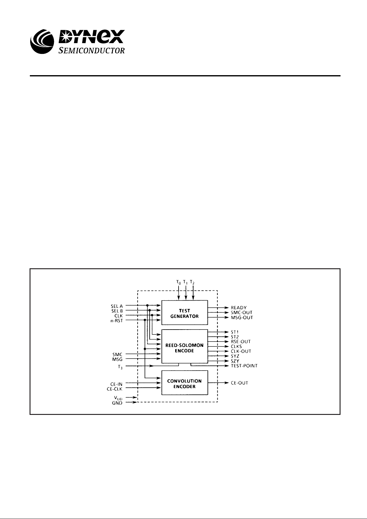
The purpose of the MA1916 is to encode serial data to
allow error correction when the data is transmitted over a noisy
communication link. As the name suggests, the unit contains
two encoding elements. The Reed-Solomon encoder appends
a checksum to a block of data, guarding against burst errors in
a message. The convolution encoder continuously creates two
code bits for each data bit it receives, increasing the noise
immunity by doubling the band width of the message. The unit
also contains a test pattern generator which can be connected
to check the functionality of the RS encoder and to provide a
message timing signal (SMC_OUT).
Protection against a long error-burst can be increased by
interleaving a number of message packets passing through
the RS encoder. The MA1916 provides pin selectable
interleave depths of 1, 4 or 5. Interleave depths of greater than
5 do not significantly improve performance.
The MA1916 is designed to conform to the CCSDS
standard for telemetry 101.0.B.2. It is manufactured in a
radiation hard low power CMOS technology. This makes it
ideal for use in satellite communications systems. The encoder
reduces the risk of data corruption and allows the designer to
minimize the transmitter power needed to establish an
effective communications link.
FEATURES
■ Radiation Hard CMOS-SOS Technology
■ Low Power Consumption
■ Latch-up Free
■ High SEU Immunity
■ CCSDS Standard RS (255, 223)
■ Selectable Interleave Depths of 1, 4 or 5
■ 5MBit/sec Input Data Rate
Figure 1: Block Diagram
MA1916
Radiation Hard Reed-Solomon
& Convolution Encoder
Replaces June 1999 version, DS3590-4.0 DS3590-5.0 January 2000
Page 2
MA1916
2/11
OPERATION
REED-SOLOMON ENCODER
The function of the Reed-Solomon (RS) encoder is to take
a block of 223 bytes of serial data and to append a checksum
of 32 bytes. The purpose of the checksum is to allow error
correction within the data block. One important feature of the
Reed-Solomon algorithm is that it allows correction of a burst
error which corrupts upto 16 consecutive bytes. If a number of
messages are interleaved this length can be increased. The
MA1916 provides pin selectable interleave depths of 1, 4 or 5
blocks (see Table 1), each of 223 bytes. An interleave depth of
5 is the maximum recommended by the CCSDS standard.
This will allow correction of up to 80 sequencial bytes in a data
packet.
The RS encoder operates from a clock input CLK which
must be driven at twice the input data rate. Internally CLK is
divided to give a clock CLKS which runs at half the frequency.
This signal is available as an output and is used to time data
into the RS encoder.
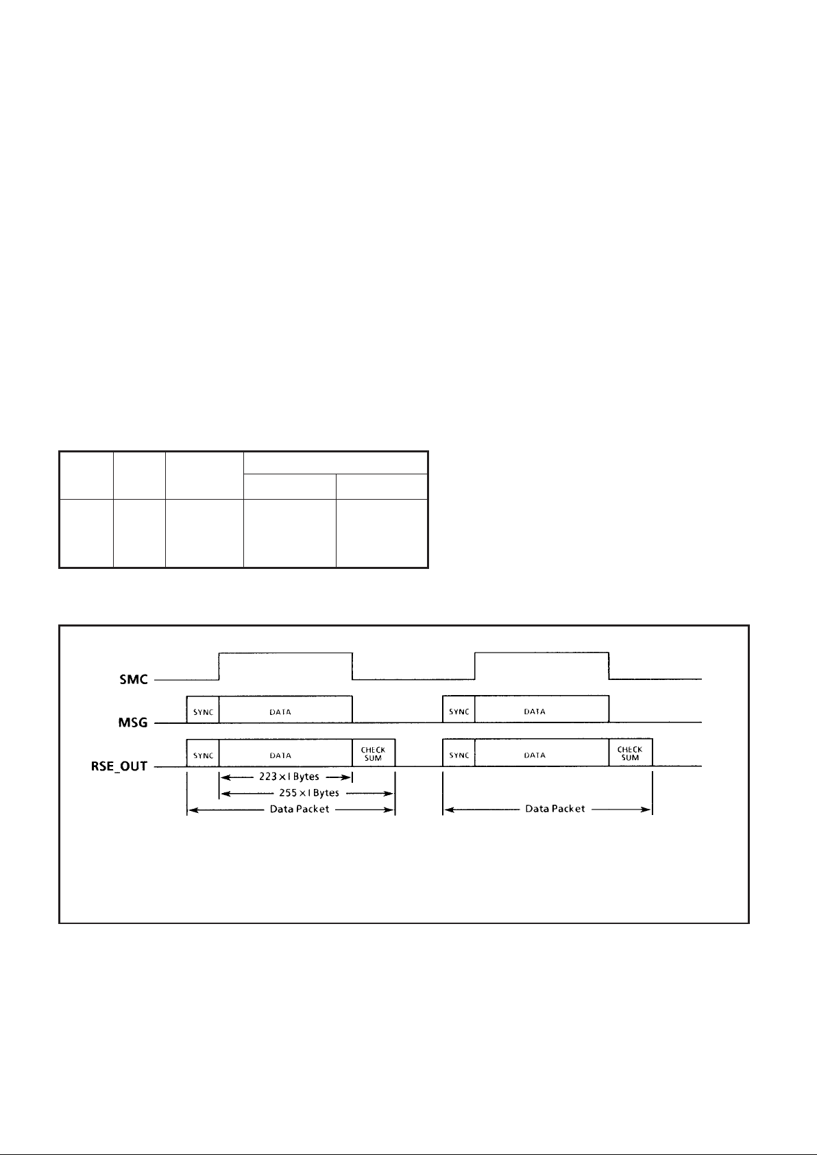
A high input on SMC is used to tell the RS encoder that
data to be encoded is present on the MSG pin (see Figure 2).
While SMC is high the data on MSG is buffered and appears
on RSE_OUT as well as being clocked into the encoder. As
soon as SMC goes low the checksum is clocked out of the
encoder onto RSE_OUT.
While SMC is high the RSE_OUT signal follows the input
MSG. When SMC is low RSE_OUT is produced from the
exclusive-OR of MSG and the checksum signal. For this
reason MSG must be held low while the encoder outputs the
checksum.
A gap can be left between successive data packets by
holding SMC and MSG low after the checksum has been sent.
Alternatively, synchronisation code can be inserted before a
data block by holding SMC low and placing the code on MSG.
As soon as SMC goes high any further data on MSG is
assumed to form part of a message and will be encoded
accordingly.
Note: External logic must guarantee the SMC is high for
the correct period, ie only while 223 x I bytes (I = interleave
depth) of data are clocked through. Otherwise when SMC falls
an invalid checksum will be produced.
SEL_A SEL_B Interleave SMC_OUT Period (Bytes)
I = Depth SMC_OUT = 1 SMC_OUT = 0
0 0 5 5 x 223 5 x 32
0 1 4 4 x 223 4 x 32
1 0 1 1 x 223 1 x 32
1 1 5 5 x 223 5 x 32
I = Interleave depths of 1, 4 or 5
SYNC: If SMC is low and no checksum is being output any data on MSG will appear on RSE_OUT.
This feature can be used to insert a synchronisation sequence before a data block.
DATA: Data block 223 x I bytes in length.
CHECKSUM: The checksum is 32 x I bytes long and appended to the data by the RS encoder.
Figure 2: Reed-Solomon Encoder Operation
Table 1: Interleave Length Defined by SEL_A and SEL_B
Page 3
MA1916
3/11
CONVOLUTION ENCODER
The convolution encoder generates 2 serial bits of output
data for each bit it reads in. The coding operates cyclically over
a length of 7 bits. It increases the bandwidth of the signal but
establishes a correlation between succesive bits in the output
signal.
The convolution encoder operates continuously using
CE_CLK to read data in on CE_IN and to write the encoded
data to CE_OUT.
If required the output of the Reed-Solomon encoder can be
fed directly into the convolution encoder by connecting
RSE_OUT to CE_ IN and CLKS to CE_CLK.
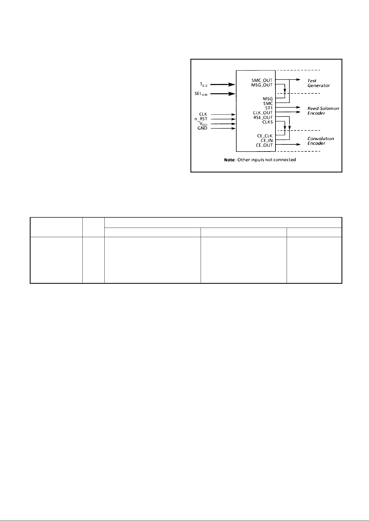
TEST GENERATOR
The MA1916 contains its own built-in test pattern
generator, this can be connected to the RS encoder for in
service testing. The test generator supplies test patterns and
the SMC signal according to the inputs on T0-2 (see Table 2)
and the interleave depth selected using SEL_A and SEL_B.
Figure 3 shows the necessary connections for feeding test
patterns through both the RS and the convolution encoder.
Figure 3: Test Configuration
Table 2: Test Pattern on MSG_OUT Defined by T0-2
PIN DESCRIPTION
VDD and GND (Power and Ground)
The MA1916 uses a single power supply of 5V ±10%.
CLK (Clock)
This input supplies a clock signal to the RS encoder and
the Test generator. It requires a signal with a nominal 50%
duty cycle running at twice the input data rate for the RS
encoder. The rising edge of CLK is used to generate the
internal CLKS signal which clocks data through the RS
encoder.
n_RST (Reset)
This active low signal is a reset supplied to the RS encoder,
the test generator and the convolution encoder. It should be
noted that the reset does not clear the check sum in the RS
encoder and a complete dummy data packet should be run
through before valid data is sent.
SEL_A and SEL_B (Interleave Depth Select)
These inputs define the interleave depth of a message
passing through the RS encoder They also specify the
message length to be produced by the test generator (see
Table 1). The inputs are connected to internal pulldown
resistors.
T
0-2
(Test Pattern Select)
These inputs select the pattern to be produced by the test
generator (see Table 2). Each input is connected to an internal
pull-down resistor.
T3 (Production Test Input)
This input is used for production testing only It has an
internal pull-down resistor and should be left unconnected .
MSG_OUT (Test Message Output)
This output pin carries the test patterns defined by the
inputs To-2 and produced by the test generator. This signal
can be connected directly to MSG for testing purposes.
Interleave Depth
T2 T1 T0 Test I = 5 (1115 bytes) I = 4 (892 bytes) I = 1 (223 bytes)
000N/A 0
0 0 1 1 (1, 2, 3, 4, 5) x 223 (1, 2, 3, 4) x 223 (1) x 223
0 1 0 2 (0) x 222 x 5, (0) x 4, (7B) (0) x 222 x 4, (0) x 3, (7B) (0) x 222, 7B
0 1 1 3 (0) x 222 x 5, (7B, AF, 99, FA, B7) (0) x 222 x4, (7B, AF, 99, FA) (0) x 222, 7B
1 0 0 4 (0) x 221 x 5, (7B) x 5, (47) x 5 (0) x 221 x 4, (7B) x 4, (47) x 4 (0) x 222, 7B
Other N/A
Page 4
MA1916
4/11
SMC_OUT (Select Message or Checksum)
This output signal is held high while the test generator clocks
out a data packet on the MSG_OUT pin. When the packet is
complete this signal goes low. It is held low for a period equal to
the time required by the RS encoder to send the corresponding
checksum. When this is complete the signal goes high and the
test generator begins a new data packet. This signal can be
connected directly to SMC for testing purposes.
READY (Test Data Valid)
This output is held low during reset and remains low for the
first complete cycle of SMC_OUT. READY rises on the second
rising edge of SMC_OUT and remains high to indicate the
presence of valid data on MSG_OUT.
CLKS (Synchronisation Clock)
This output clock runs at half the speed of the input clock
CLK. CLKS remains low after n_RST is raised until SMC is
raised, SMC being captured on the falling edge of CLK (timing
4). CLKS then changes state on the rising edge of each CLK
cycle regardless of the state of SMC. The signal is used to
clock data into and out of the RS encoder.
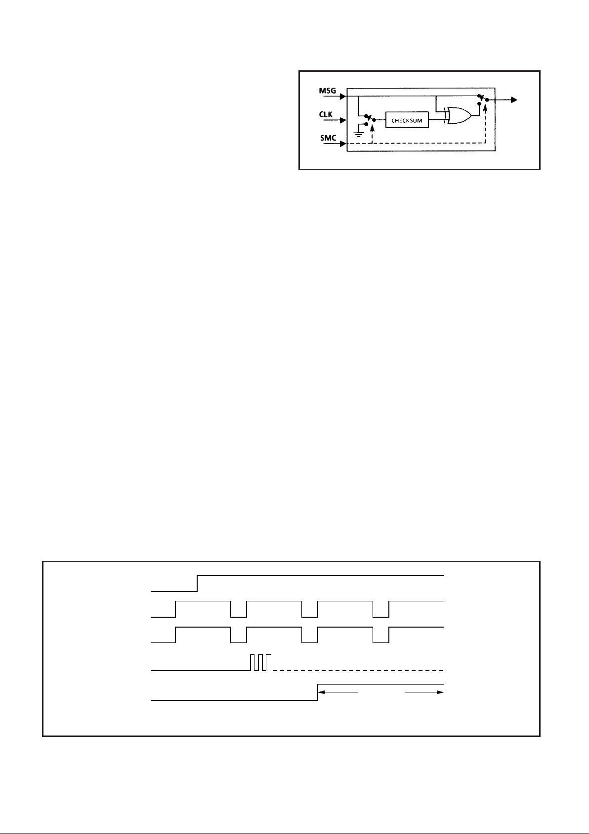
MSG (Message)
MSG is the data input to the RS encoder. Each bit is read in
on the rising edge of CLKS. While the SMC signal is high data
on the input passes directly to the output RSE_OUT. While
SMC is low RSE_OUT is the logical XOR of the MSG input and
the output of the check-sum generator. Therefore MSG must
be held low while the RS encoder is clocking out the check
sum (see Figure 4).
SMC (Select Message or Checksum)
While the SMC input is high, data on the MSG pin is
clocked into the RS encoder. SMC is held high for a period
dictated by the interleave depth being used (see Table 1).
When SMC falls the RS encoder begins to clock out the
checksum for the preceeding data. SMC should be held low
until the complete checksum has been output. The rising edge
of SMC indicates the start of a new data block to be encoded.
RSE_OUT (Reed-Solomon Encoder Output)
This signal outputs the completed data packet comprised
of the message followed by its associated checksum block.
The data is valid on the rising edge of CLKS.
Figure 4: Reed-Solomon Encoder
ST1 (RS Encoder Output Valid)
This output is set low during a reset and goes high when
sufficient dummy data has been clocked through the RS
encoder to clear it (see Figure 5).
SYZ (Byte Rate Clock)
SYZ is a byte rate clock output derived from CLKS. It is
high during every eighth period of CLKS and low at other
times.
SZY (Byte Rate Clock)
SZY is a byte rate clock output derived from CLKS. It is low
during every eighth period of CLKS and high at other times. It
is the inverse of SYZ.
ST2 (Production Test Output)
The output is used for production testing and should be left
unconnected.
TEST_POINT (Production Test Output)
This output is used for production testing and should be left
unconnected.
CE_IN (Convolution Encoder Data In)
This input is used to read data into the convolution
encoder. The state of CE_IN is read on the rising edge of
CE_CLK.
Figure 5: Reed-Solomon Encoder Operation
SMC
MSG
CLKS
ST1
n_RST
Output Valid
Note: ST1 rises on the second rising edge of SMC following n_RST high.
CLKS starts toggling on the first rising edge of SMC following n_RST high.
Page 5

MA1916
5/11
DC CHARACTERISTICS AND RATINGS
Parameter Min Max Units
Supply Voltage -0.5 7 V
Input Voltage -0.3 VDD+0.3 V
Current Through Any Pin -20 +20 mA
Operating Temperature -55 125 °C
Storage Temperature -65 150 °C
CE_CLK (Convolution Encoder Clock)
The CE_CLK input drives the timing of the convolution
encoder. Data is read in on CE_IN on the rising edge of
CE_CLK and output on CE_OUT on both the rising and falling
edge of CE_CLK.
Note: The output data rate is twice the input data rate.
A 50% duty cycle clock is required. If this is provided by the
CLKS output, data can be read directly from RSE_OUT to the
CE_IN input (see figure 3).
CE_OUT (Convolution Encoder Output)
This signal carries the output data from the convolution
encoder. The data rate on CE_OUT is twice that of CE_IN.
CLK_OUT (Clock Out)
CLK_OUT is a buffered output of the CLK input signal. If
CLKS is connected to CE_CLK to drive the convolution
encoder, CE_OUT can be captured on the falling edge of
CLK_OUT.
Note: Stresses above those listed may cause permanent
damage to the device. This is a stress rating only and
functional operation of the device at these conditions, or at
any other condition above those indicated in the operations
section of this specification, is not implied. Exposure to
absolute maximum rating conditions for extended periods
may affect device reliability.
Table 3: Absolute Maximum Ratings
Symbol Parameter Conditions Min Typ Max Units
V
DD
Supply Voltage - 4.5 5.0 5.5 V
V
IH
CMOS Input High Voltage VDD = 5.5V 0.8 V
DD
-VDDV
V
IL
CMOS Input Low Voltage VDD = 5.5V V
SS
- 0.2 V
DD
V
V
OH
CMOS Output High Voltage VDD = 5V, IOH = -1.0mA VDD-0.5 - - V
V
OL
CMOS Output Low Voltage VDD = 5V, IOL = 4.0mA - - 0.4 V
I
IL
Input Leakage Current VDD = 5.5V, VIN = VSS or V
DD
-10 - 10 µA
I
PDL
Input Pull-Down Current VDD = 5.5V, VIN = VSS or V
DD
-20 - 150 µA
I
DD1
Static Power Supply Current VDD = 5.5V - 0.1 2.5 mA
I
DD2
Dynamic Power Supply Current CLK = 10MHz, VDD = 5.5V - 3 10 mA
Notes: 1. VDD = 5V±10%, over full operating temperature range. 2. Total dose radiation not exceeding 1x10⁵ Rads(Si)
3. Mil-Std-883, method 5005, subgroups 1, 2, 3
Table 4: DC Electrical Characteristics
AC CHARACTERISTICS
No. Parameter Min. Max. Units
1 CLK hlgh to CLKS - 25 ns
2 CLK high to SYZ or SZY - 30 ns
3 SMC hold after CLK low 0 - ns
4 SMC setup to CLK low 30 - ns
5 MSG set up to CLKS high 10 - ns
6 MSG hold after CLKS high 10 - ns
7 MSG to RSE_OUT propagation delay - 30 ns
8 CLKS to RSE_OUT (SMC low) - 25 ns
9 CLK to CLK_OUT propagation delay - 25 ns
10 CE_IN setup to CE_CLK hlgh 10 - ns
11 CE_IN hold after CE_CLK high 10 - ns
12 CE_CLK to CE_OUT - 25 ns
13 CLK CYCLE TIME 100 - ns
Table 5: AC Electrical Characteristics
Note: Mil-Std-883, method 5005,
subgroups 9, 10, 11
Page 6

MA1916
6/11
Symbol Parameter Conditions Min. Typ. Max. Units
C
IN
Input Capacitance Vl = 0V - 3 5 pF
C
OUT
Output Capacitance V
I/O
= 0V - 5 7 pF
Note: T
A
= 25°C and f = 1MHz. Data obtained by characterisation or analysis; not routinely measured.
Table 6: Capacitance
Symbol Parameter Conditions
F
T
Functionality VDD = 4.5V - 5.5V, Frequency = 1MHz
VIL = VSS, VIH = VDD, VOL = VOH = VDD/2
Temperature = -55°C to +125°C, Radiation to 1MRad Total Dose
Mil-Std-883, method 5005, subgroups 7, 8A, 8B
Table 7: Functionality
Subgroup Definition
1 Static characteristics specified in Table 4 at +25°C
2 Static characteristics specified in Table 4 at +125°C
3 Static characteristics specified in Table 4 at -55°C
7 Functional characteristics specified in Table 7 at +25°C
8A Functional characteristics specified in Table 7 at +125°C
8B Functional characteristics specified in Table 7 at -55°C
9 Switching characteristics specified in Table 5 at +25°C
10 Switching characteristics specified in Table 5 at +125°C
11 Switching characteristics specified in Table 5 at -55°C
Table 8: Definition of Subgroups
Page 7

MA1916
7/11
TIMING DIAGRAMS
Note: Bytes of MSG labelled 0 to 222 x I
Bytes of RSE_OUT labelled 0 to 254 x I
Bits labelled 0 to 7
I = Interleave depth of 1, 4 or 5
* User can capture RSE_OUT on rising edge of CLKS
Figure 6: RS Encoder Timings
*
Notes: 1. If CE_CLK is driven by CLKS, the user can capture CE_OUT on the falling edge of CLK_OUT.
2. Arrows show which O/P bits correspond to which I/P bit.
See Note 2
Figure 7: Convolution Encoder Timings
Page 8

MA1916
8/11
Figure 8: 28-Lead Ceramic DIL (Solder Seal) - Package Style C
OUTLINES AND PIN ASSIGNMENTS
Ref
Millimetres Inches
Min. Nom. Max. Min. Nom. Max.
A - - 5.715 - - 0.225
A1 0.38 - 1.53 0.015 - 0.060
b 0.35 - 0.59 0.014 - 0.023
c 0.20 - 0.36 0.008 - 0.014
D - - 36.02 - - 1.418
e - 2.54 Typ. - - 0.100 Typ. -
e1 - 15.24 Typ. - - 0.600 Typ. -
H 4.71 - 5.38 0.185 - 0.212
Me - - 15.90 - - 0.626
Z - - 1.27 - - 0.050
W - - 1.53 - - 0.060
XG404
D
W
A
e b Z
H
A
1
15°
M
E
C
e
1
Seating Plane
114
2815
TOP VIEW
Page 9

MA1916
9/11
Figure 9: 28-Lead Ceramic Flatpack (Solder Seal) - Package Style F
Ref
Millimetres Inches
Min. Nom. Max. Min. Nom. Max.
A - - 3.18 - - 0.125
Q 0.66 - - 0.026 - -
b 0.38 - 0.48 0.015 - 0.019
c 0.10 - 0.18 0.004 - 0.007
D 18.08 - 18.49 0.712 - 0.728
e - 1.27 - - 0.050 -
L 7.62 - 9.91 0.300 - 0.390
M 12.50 - 12.09 0.492 - 0.508
XG530
M
b
e
D
L
A
Q
c
Pin 1
Z
M
E
Page 10

MA1916
10/11
Figure 10: Flatpack Pinout
1T2
2T1
3 CE_CLKS
4 CE_IN
5 CE_OUT
6 TEST_POINT
7 N/C
8 ST1
9 GND
10 SEL_A
11 STZ
12 SEL_B
13 SZY
14 n_RST
28
MSG_OUT
27
CLK_OUT
26
SMC
25
RSE_OUT
24
SYZ
23
T3
22
CLKS
21
VDD
20
N/C
19
T0
18
MSG
17
CLK
16
READY
15
SMC_OUT
Bottom
View
RADIATION TOLERANCE
Total Dose Radiation Testing
For product procured to guaranteed total dose radiation
levels, each wafer lot will be approved when all sample
devices from each lot pass the total dose radiation test.
The sample devices will be subjected to the total dose
radiation level (Cobalt-60 Source), defined by the ordering
code, and must continue to meet the electrical parameters
specified in the data sheet. Electrical tests, pre and post
irradiation, will be read and recorded.
Dynex Semiconductor can provide radiation testing
compliant with Mil-Std-883 test method 1019, Ionizing
Radiation (Total Dose).
Total Dose (Function to specification)* 1x10⁵ Rad(Si)
Transient Upset (Stored data loss) 5x10¹⁰ Rad(Si)/sec
Transient Upset (Survivability) >1x10
12
Rad(Si)/sec
Neutron Hardness (Function to specification) >1x10¹⁵ n/cm
2
Single Event Upset** <1x10
-10
Errors/bit day
Latch Up Not possible
* Other total dose radiation levels available on request
** Worst case galactic cosmic ray upset - interplanetary/high altitude orbit
Table 9: Radiation Hardness Parameters
Page 11

MA1916
11/11
Unique Circuit Designator
S
R
Q
H
Radiation Hard Processing
100 kRads (Si) Guaranteed
300 kRads (Si) Guaranteed
1000 kRads (Si) Guaranteed
Radiation Tolerance
C
F
L
Ceramic DIL (Solder Seal)
Flatpack (Solder Seal)
Leadless Chip Carrier
Package Type
QA/QCI Process
(See Section 9 Part 4)
Test Process
(See Section 9 Part 3)
Assembly Process
(See Section 9 Part 2)
L
C
D
E
B
S
Rel 0
Rel 1
Rel 2
Rel 3/4/5/STACK
Class B
Class S
Reliability Level
MAx1916xxxxx
For details of reliability, QA/QC, test and assembly
options, see ‘Manufacturing Capability and Quality
Assurance Standards’ Section 9.
ORDERING INFORMATION
CUSTOMER SERVICE CENTRES
France, Benelux, Italy and Spain Tel: +33 (0)1 69 18 90 00. Fax: +33 (0)1 64 46 54 50
North America Tel: 011-800-5554-5554. Fax: 011-800-5444-5444
UK, Germany, Scandinavia & Rest Of World Tel: +44 (0)1522 500500. Fax: +44 (0)1522 500020
SALES OFFICES
France, Benelux, Italy and Spain Tel: +33 (0)1 69 18 90 00. Fax: +33 (0)1 64 46 54 50
Germany Tel: 07351 827723
North America Tel: (613) 723-7035. Fax: (613) 723-1518. Toll Free: 1.888.33.DYNEX (39639) /
Tel: (831) 440-1988. Fax: (831) 440-1989 / Tel: (949) 733-3005. Fax: (949) 733-2986.
UK, Germany, Scandinavia & Rest Of W orld Tel: +44 (0)1522 500500. Fax: +44 (0)1522 500020
These offices are supported by Representatives and Distributors in many countries world-wide.
© Dynex Semiconductor 2000 Publication No. DS3590-5 Issue No. 5.0 January 2000
TECHNICAL DOCUMENTATION – NOT FOR RESALE. PRINTED IN UNITED KINGDOM
HEADQUARTERS OPERATIONS
DYNEX SEMICONDUCTOR LTD
Doddington Road, Lincoln.
Lincolnshire. LN6 3LF. United Kingdom.
Tel: 00-44-(0)1522-500500
Fax: 00-44-(0)1522-500550
DYNEX POWER INC.
Unit 7 - 58 Antares Drive,
Nepean, Ontario, Canada K2E 7W6.
Tel: 613.723.7035
Fax: 613.723.1518
Toll Free: 1.888.33.DYNEX (39639)
This publication is issued to provide information only which (unless agreed by the Company in writing) may not be used, applied or reproduced for any purpose nor form part of any order or contract nor to be regarded
as a representation relating to the products or services concerned. No warranty or guarantee express or implied is made regarding the capability, performance or suitability of any product or service. The Company
reserves the right to alter without prior notice the specification, design or price of any product or service. Information concerning possible methods of use is provided as a guide only and does not constitute any
guarantee that such methods of use will be satisfactory in a specific piece of equipment. It is the user's responsibility to fully determine the performance and suitability of any equipment using such information and
to ensure that any publication or data used is up to date and has not been superseded. These products are not suitable for use in any medical products whose failure to perform may result in significant injury
or death to the user. All products and materials are sold and services provided subject to the Company's conditions of sale, which are available on request.
All brand names and product names used in this publication are trademarks, registered trademarks or trade names of their respective owners.
http://www.dynexsemi.com
e-mail: power_solutions@dynexsemi.com
Datasheet Annotations:
Dynex Semiconductor annotate datasheets in the top right hard corner of the front page, to indicate product status. The annotations are as follows:-
Target Information: This is the most tentative form of information and represents a very preliminary specification. No actual design work on the product has been started.
Preliminary Information: The product is in design and development. The datasheet represents the product as it is understood but details may change.
Advance Information: The product design is complete and final characterisation for volume production is well in hand.
No Annotation: The product parameters are fixed and the product is available to datasheet specification.
 Loading...