

Page 1
MA17503
1/34
The MA17503 Interrupt Unit is a component of the MAS281
chip set. Other chips in the set include MA17501 Execution Unit
and the MA17502 Control Unit. Also available is the peripheral
MA31751 Memory Management/Block Protection Unit. The
lnterrupt Unit, in conjunction with these additional chips,
implements the full MIL-STD-1750A Instruction Set
Architecture.
The MA17503 - consisting of the Pending Interrupt
Register, Mask Register, Interrupt Priority Encoder, Fault
Register, Timer A, Timer B, Trigger-Go Counter, Bus Fault
Timer, and DMA interface - handles all interrupt fault, and DMA
interfacing, in addition to providing all three hardware timers.
The Interrupt Unit also implements 26 of the MIL-STD-1750A
specified l/O commands. Table 1 provides brief signal
definitions.
The MA17503 is offered in dual-in-line, flatpack or leadless
chip carrier packaging. Screening and packaging options are
described at the end of this document.
FEATURES
■ Mil-Std-1750A Instruction Set Architecture
■ Full Performance over Military Temperature Range (-55°C
to +125°C)
■ Radiation Hard CMOS/SOS Technology
■ Interrupt Handler
• 9 User Interrupt Inputs
• Pending Interrupt Register
• Interrupt Mask Register
• Interrupt Priority Encoder
■ Fault Handler
• 8 User Faults Inputs
• Fault Register
■ Timers
• Timer A
• Timer B
■ Trigger-Go
■ DMA Interface
■ Interface Discretes
• Normal Power-Up
• Start-Up ROM Enable
• Configuration Word Enable
■ Implements 26 MIL-STD-1750A Specified l/O Commands
■ MAS281 Integrated Built-ln Self Test
■ TTL Compatible System Interface
BLOCK DIAGRAM
MA17503
Radiation Hard MIL-STD-1750A Interrupt Unit
Replaces June 1999 version, DS3566-4.0 DS3566-5.0 January 2000
Page 2

MA17503
2/34
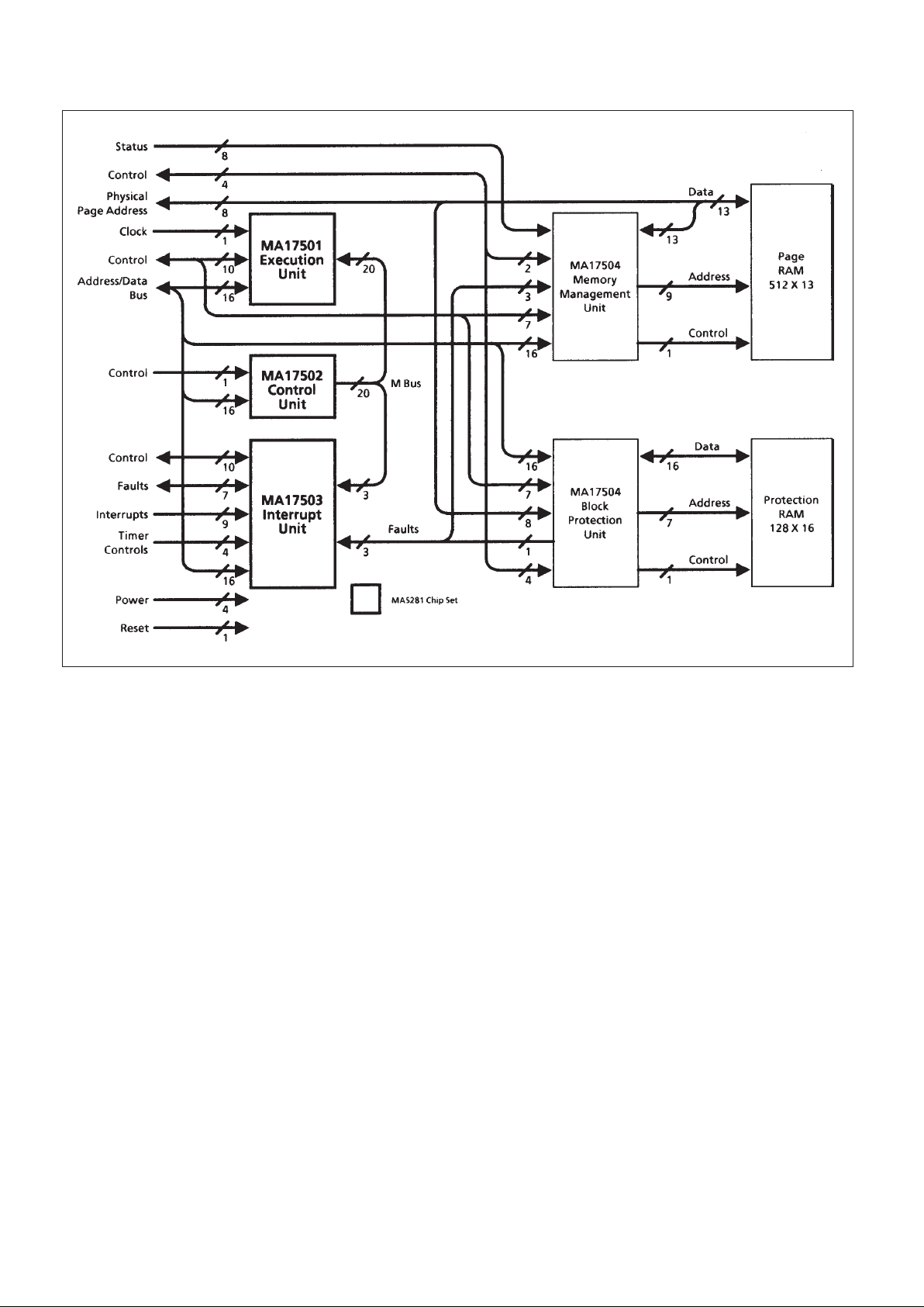
1.0 SYSTEM CONSIDERATIONS
The MA17503 Interrupt Unit (IU) is a component of the GPS
MAS281 chip set. This chip set implements the full MIL-STD1750A instruction set architecture. Other chips in the set
include the MA17501 Execution Unit (EU) and MA17502
Control Unit (CU). Also available is the peripheral MA31751
Memory Management Unit/Block Protection Unit (MMU(BPU)).
Figure 1 depicts the relationship between the chip set
components.
The IU provides the interrupt and fault handling interfaces
for the chip set. The IU also provides the DMA control interface
logic, contains interval Timers A and B, the Trigger-Go
Counter, the Bus Fault Timeout timer, and decodes all MILSTD-1750A specified l/O commands in support of these
functions. The EU provides the arithmetic and logical
computation resources for the chip set. The EU and IU are each
controlled by microcode from the CU. The MMU(BPU) may be
configured to provide either 1M-word memory management
(MMU) and/or 1K-word memory block write protection (BPU)
functions.
As shown in Figure 1, the MAS281 is the minimum
processor configuration consisting of an Execution Unit, a
Control Unit, and an Interrupt Unit. This configuration is
capable of accessing a 64K-word address space. Addition of a
MMU configured MA31751 allows access to a 1M-word
address space. Addition of a BPU configured MA31751
provides hardware support for 1K-word memory block write
protection.
The IU, as with all components of the MAS281 chip set, is
fabricated with CMOS/SOS process technology.
Detailed descriptions of the lUs companion chips are
provided in separate data sheets. Additional discussions on
chip set system considerations, interconnection details, and
Digital Avionics Instruction Set (DAIS) mix benchmarking
analysis are provided in separate application notes.
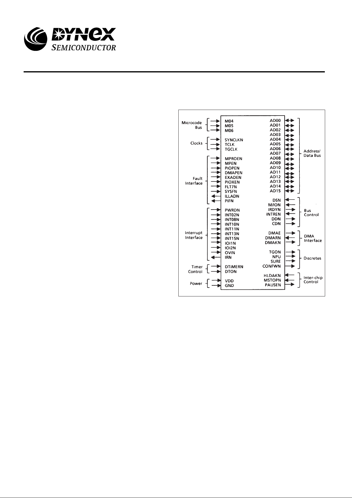
SIGNAL I/O DEFINITION
AD00 - AD15 I/O/Z 16-Bit Address/Data Bus
M04, M05, M06 I 3 Bits of the Mlcrocode Instruction
Word
INTREN I Interrupt Unit Microcode Interface
Enable
DMAKN O DMA Request Acknowledge
DMAE O DMA Interface Enable
DMARN I DMA Request
M/ION I Memory/lnput-Output
DSN I Data Strobe
SYNCLKN I Synchronisation Clock
IRDYN O Interrupt Unit Ready
DDN O Data Transceiver Dlrection Control
CDN O Control Bus Transceiver Direction
Control
SYSFN I System Fault
FLT7N I Fault 7 (Undefined Fault)
PIOXEN I Programmed I/O Transfer Error
EXADEN I External Address Error
DMAPEN I DMA Parity Error
PIOPEN I Programmed I/O Parity Lrror
MPEN I Memory Parity Error
MPROEN I Memory Protection Error
ILLADN O Illegal Address
PIFN O Instruction Abort
PWRDN I Power-Down Interrupt
INT02N I Level 2 Interrupt
INT08N I Level 8 Interrupt
INT10N I Level 10 Interru pt
INT11N I Level 11 Interrupt
IOI1N I I/O Register Interrupt 1
INT13N I Level 13 Interrupt
IOI2N I I/O Register Interrupt 2
INT15N I Level 15 Interrupt
OV1N I Fixed-Point Overflow Interrupt
IRN O Interrupt Request
TCLK I Clock for Tlmers A and B
TGCLK I Trigger Go Timer Clock
DTIMERN I Disable Timers
DTON I Disable Bus-Fault Timeout
TGON O Trigger-Go Timer Overflow
NPlJ O Normal Power-up Indicator
SURE O Start-up ROM Enable
CONFWN O Configuration Word Enable
HLDAKN I Hold Acknowledge
MSTOPN I Microcode Stop
PAUSE O Processor Pause
VDD I Power
GND I Ground
Table 1: Signal Definitions
Page 3
MA17503
3/34
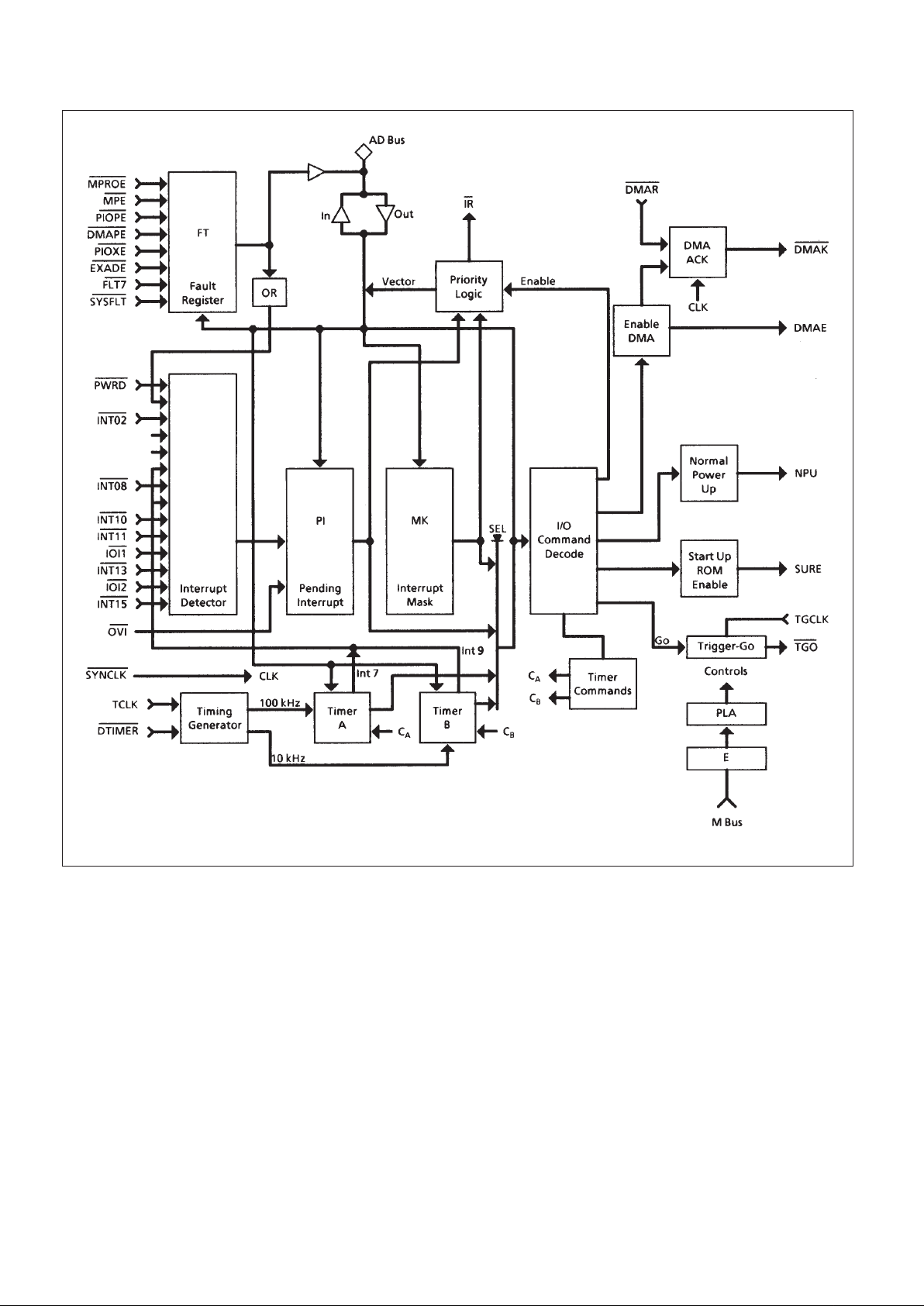
2.0 ARCHITECTURE
The Interrupt Unit consists of a Pending Interrupt Register,
Mask Register, Interrupt Priority Encoder, Fault Register, two
interval timers, two watchdog timers, DMA Control interface,
and both microcode and internal I/O instruction decode logic.
Details of these components are depicted in Figure 2 and are
discussed below:
2.1 PENDING INTERRUPT REGISTER
The Pending Interrupt Register (Pl) is the dedicated 16-bit
register that latches all pending interrupt requests and stores
them until serviced. The inputs to the Pl are buffered by fallingedge detectors to prevent repeat latching of interrupt requests
held low longer than required. The Pl supports nine external
interrupts inputs and seven chip set generated interrupts. The
output of the Pl is ANDed with the Mask Register to create the
interrupt request (IRN) signal for the MA17502 Control Unit. A
one in a Pl bit position indicates an interrupt is pending and the
interrupt level is equal to the bit position.
2.2 MASK REGISTER
The Mask Register (MK) is the dedicated 16-bit register
containing the information that filters the Pl output to the Priority
Encoder and the IRN generation logic. A one in a MK bit
position allows the interrupt request, of the same bit position in
the Pl, to enter the Priority Encoder and cause IRN to drop low.
Pl bits 1 - 4 and 6 - 15 are maskable.
2.3 INTERRUPT PRIORITY ENCODER
The Interrupt Priority Encoder accepts the enabled, mask
filtered, output of the Pl and generates a four bit code
designating the level of the highest priority pending interrupt.
Level zero (Pl bit zero) has the highest priority and level 15 (Pl
bit 15) the lowest. The four bit priority code is placed on the AD
Bus during the microcoded interrupt handling routine.
2.4 FAULT REGISTER
The Fault Register (FT) is the dedicated 16-bit register that
latches the 15 specified (fault 12 is reserved) faults. The FT
supports eight external Fault inputs and three chip-set
generated Faults. The output of the FT is ORed together,
buffered by a falling-edge detector, and input to the Pl to
generate the level one interrupt. FT bits 13 - 15 are used to
indicate the results of the MAS281 BlT. Once the FT has
latched a fault, it can only be cleared via internal l/O command
(individual fault bits cannot be cleared).
Figure 1
Page 4
MA17503
4/34
Figure 2: MA17503 Interrupt Unit Architecture
Page 5

MA17503
5/34
Anti-repeat logic between the FT and Pl prevents latching
more than a single interrupt into the Pl before the user interrupt
service routine has cleared the FT. The microcoded interrupt
service routine reads the interrupt priority vector from the
Interrupt Unit and clears the serviced interrupt from the Pl. At
this point the Pl is ready to latch another interrupt into this bit.
When this microcoded service routine acts on a level 1
interrupt, it clears the Pl bit 1, but the FT maintains the
interrupting fault bit(s). Therefore, a level 1 interrupt would be
latched again if there were no anti-repeat logic to prevent a
never ending loop of interrupts from occurring.
Interrupts are serviced at the end of the currently executing
instruction if not masked and if interrupts are enabled. System
software servicing level 1 interrupts must clear the FT via the
RCFR internal l/O command at some point in the routine to
allow subsequent faults to latch a level 1 interrupt request. A
non-destructive read of the FT is provided by the internal I/O
command RFR, but this command should be used carefully.
2.5 INTERVAL TIMERS
The Interrupt Unit contains both MIL-STD-1750A 16-bit
interval timers, A and B. The TCLK input is synchronized with
SYNCLKN and increments Timer A once a TCLK period. Timer
B is incremented by the synchronized TCLK divided by 10.
Timer A overflow sets Pl bit 7 and Timer B overflow sets Pl bit 9.
The timers are controlled via the l/O command decode logic, or
they can be disabled via the DTlMERN input.
2.6 WATCHDOG TIMERS
The Interrupt Unit contains two watchdog timers, TriggerGo and Bus Fault. The Bus Fault timer assures timely
completion of all AD Bus cycles by terminating bus cycles over
two TCLK (maximum, minimum one TCLK period) periods in
duration. This function is automatic, but can be disabled by
DTON low. FT bit 5 or 8 is set for terminated l/O transfers or
memory transfers, respectively, when the Bus Fault timer
expires.
The Trigger-Go timer is an autonomous 16-bit ripple
counter incremented by TGCLK. Upon power-up, the TriggerGo timer begins to count. The GO l/O command resets the
timer, thus preventing it from overflowing and causing TGON to
drop low. The DTIMERN input prevents the Trigger-Go timer
from incrementing.
2.7 DMA CONTROL INTERFACE
The DMA control interface logic is contained in the Interrupt
Unit. The interface is composed of the three signals: DMAE,
DMARN, and DMAKN. If the interface is enabled, an internal
l/O command raises DMAE high to indicate the MAS281’s
readiness to accept DMA transfer requests (DMARN low). A
subsequent low on DMARN causes the lU to respond with
DMAKN low. DMAKN low halts the processor and places all AD
Bus and bus control lines in the high-impedance state. Control
is returned to the MAS281 when DMARN is pulled high again.
DTIMERN is the user available way to disable the DMA
interface.
2.8 INTERNAL I/O COMMAND DECODE LOGIC
The Interrupt Unit implements the 26 MIL-STD-1750A
specified l/O command functions listed in Table 2. The lU also
decodes an additional 386 commands that are implemented in
the MMU(BPU) and the two Status Word XlO commands that
are handled in microcode for AD Bus control. The lU continually
monitors AD Bus traffic. When M/lON is low, the lU latches the
information present on the AD Bus during the address portion
of the bus cycle. This information is subsequently decoded and
creates the appropriate control signals to perform the l/O
command function.
2.9 MICROCODE DECODE LOGIC
The microcode decode logic can be split into command and
control functions. Microcode instruction bits 4, 5 and 6 are
decoded as commands for the FT, the interrupt interface, the
DMA interface, and the discrete output signal, NPU. The
microcode command interface is enabled when lNTREN is
pulled low and is disabled during DMA and the Hold state.
Microcode bits 5 and 6 provide control of DDN during memory
read and write cycles, and external l/O cycles.
Operation Command Mnemonic
Code (Hex)
Output
Set Fault Register 0401 SFR
Set Interrupt Mask 2000 SMK
Clear Interrupt Request 2001 CLIR
Enable Interrupts 2002 ENBL
Dlsable Interrupts 2003 DSBL
Reset Pending Interrupt 2004 RPI
Set Pending Interrupt Reglster 2005 SPI
Reset Normal Power Up Discrete 200A RNS
Write Status Word 200E WSW
Enable Start Up ROM 4004 ESUR
Disable Start up ROM 4005 DSUR
Direct Memory Access Enable 4006 DMAE
Direct Memory Access Disable 4007 DMAD
Timer A Start 4008 TAS
Timer A Halt 4009 TAH
Output Timer A 400A OTA
Reset Tngger-Go 400B GO
Timer B Start 400C TBS
Timer B Halt 400D TBH
Output Timer B 400E OTB
Input
Read Configuration Word 8400 RCW
Read Fault Register Wlthout Clear 8401 RFR
Read Interrupt Mask A000 RMK
Read Pending Interrupt Reglster A004 RPIR
Read Status Word A00E RSW
Read and Clear Fault Reylster A00F RCFR
Input Timer A C00A ITA
Input Tlmer B C00E ITB
Page 6

MA17503
6/34
3.0 INTERFACE SIGNALS
All signals comply with the voltage levels of Table 1. In
addition, each of these functions is provided with Electrostatic
Discharge (ESD) protection diodes. All unused inputs must be
held to their inactive state via a connection to VDD or GND.
Throughout this data sheet, active low signals are denoted
by either a bar over the signal name or by following the name
with an “N’’ suffix (e.g., DMAKN). Referenced signals that are
not found on the MA17503 are preceded by the originating
chip’s functional acronym in parentheses (e.g., (EU)OSC).
Following is a description of each pin function grouped
according to functional interface. The function name is
presented first, followed by its acronym, its type, and its
description. Function type is either input, output, high
impedance (Hi-z), or a combination thereof. Timing
characteristics of each of the functions described is provided in
Section 5.0.
3.1 POWER LNTERFACE
The power interface consists of one 5V VDD connection
and one GND connection.
3.2 CLOCKS
The clock interface, discussed below, provides
synchronization for lnterrupt Unit operations and the clock
inputs for the interval and watchdog timers.
3.2.1 Synchronisation Clock (SYNCLKN)
Input. The MA17501 Execution Unit (EU) generates the
SYNCLKN signal for the Interrupt Unit. The Interrupt Unit uses
this signal to synchronise system inputs (e.g., interrupts and
faults) to the MAS281 machine cycle and to control all other
internal functions.
3.2.2 Timer Clock (TCLK)
Input. TCLK is a 100 KHz, user provided clock signal that
drives the interval timers A and B, and the Bus Fault timer.
TCLK is synchronised to the MAS281 machine cycle, via
SYNCLKN, before being sent to the interval timers. This allows
the lU to implement the Internal l/O Commands associated with
timer operation.
The synchronised version of TCLK drives interval timer A,
clocking it once every 10 microseconds. The synchronised
TCLK is divided by 10 to provide a 10 KHz clock for driving
interval timer B, clocking it once every 100 microseconds.
The unsynchronised TCLK is used to increment the Bus
Fault watchdog timer. When DSN drops low, the Bus Fault
timer is enabled to count and expires after two TCLK high-tolow transitions.
3.2.3 Trigger-Go Clock (TGCLK)
Input. This user provided clock drives the autonomous onchip system watchdog timer. The Trigger-Go timer is
incremented by the high-to-low transition of TGCLK.
3.3 BUSES
Following is a discussion of the two communication buses
connecting the lnterrupt Unit to the rest of the three chip set.
The AD Bus transfers 16-bit data and commands, while the M
Bus communicates microcode control data.
3.3.1 Address/Data Bus (AD Bus)
Input/Output/Hi-z. These signals comprise the multiplexed
address and data bus. During internal bus operations, the AD
Bus accommodates the transfer of Internal I/O commands and
data from the MA17501 Execution Unit to the lnterrupt Unit. lt
also accommodates the transfer of data from the lnterrupt Unit
to the Execution Unit in response to internal I/O commands.
AD00 is the most significant bit position and AD15 is the least
significant bit position of both the 16-bit data and 16-bit
command. A high on this bus corresponds to a logic 1 and a low
corresponds to a logic 0.
Commands on the AD Bus are passed through transparent
latches during the low state of input/output SYNCLKN cycles
and are latched at the low-to-high transition of SYNCLKN. Data
on the AD Bus, is either clocked into the lU by the high-to-low
transition of SYNCLKN or placed there by the lU during the low
portion of SYNCLKN.
3.3.2 Microcode Bus Bits 4, 5 and 6 (M04, 05 & 06)
Inputs. M04, M05, M06 are bits 4, 5 and 6 of the 20-bit
Microcode Bus and are coded in the 40-bit microcode
instruction as bits 4, 5 and 6. These bits are latched into the IU
at the SYNCLKN high-to-low transition and are decoded for
commanding the Fault Register, the DMA interface, the NPU
discrete, and for providing the 4-bit priority encoded interrupt
vector to the EU. lU microcode command cycles are extended
to six (EU)OSC cycles by INTREN low. Microcode bits 5 and 6
provide control of DDN during memory and external I/O cycles.
The microcode bus is not latched during DMA or the Hold state
(DMAKN or HLDAKN low).
3.4 BUS CONTROL
The following is a discussion of the signals used to control
the AD Bus and M Bus. They enable the respective busses at
the proper time and control system access to the MAS281
System AD Bus.
3.4.1 Data Strobe (DSN)
Input. The Interrupt Unit receives DSN from the Execution
Unit. The DSN high-to-low transition starts the Bus Fault
watchdog timer and during successful bus data transfers, the
low-to-high transition halts and resets the Bus Fault watchdog
timer. DSN is also instrumental in controlling the DDN signal
during MAS281 Read/lnput bus cycles.
3.4.2 Memory/lnput-Output (M/ION)
Input. The Interrupt Unit receives M/ION from the Execution
Unit. M/ION low enables l/O command decoding logic M/ION
also selects the FT bit to set in response to a low on MPROEN
and EXADEN.
3.4.3 Interrupt Unit Ready (IRDYN)
Output. The Interrupt Unit uses the IRDYN signal to cause
the Execution Unit clock generation state machine to inject one
wait state into lnternal I/O machine cycles, thus causing the
minimum five (EU)OSC period machine cycle to be extended to
a six (EU)OSC period 50% duty cycle machine cycle. Internal
l/O machine cycles occur during execution of the lU
implemented l/O commands listed in Table 2.
Page 7

MA17503
7/34
3.4.4 Interrupt Unit Microcode Enable (INTREN)
lnput. The Execution Unit provides lNTREN to the lnterrupt
Unit to enable the microcode command interface. When
INTREN is low, microcode instruction bits 4, 5 and 6 (latched
into the lU microcode register at the SYNCLKN high-to-low
transition, if HLDAKN and DMAKN are high) are decoded by
the lU as commands for the FT, NPU discrete, internal DMA
interface, and interrupt vectoring. lNTREN low causes the EU
to extend the machine cycle to six (EU)OSC periods.
3.4.5 Data Transceiver Direction (DDN)
Output. DDN is provided to control the directionality of the
AD/Data Bus transceivers. DDN is high during data transfers
from the MAS281 to the user system and when it is necessary
to keep the transceivers from driving the MAS281 System AD
Bus. DDN is low during transfers from the user system to the
MAS281.
Cycles during which DDN is high include: memory writes,
outputs, IU implemented Internal l/O command execution
(except Read Configuration Word (RCW)), and all MA17504
MMU(BPU) implemented l/O command execution.
Cycles during which DDN is low include: memory reads
(data portion), inputs (data portion), the Configuration Word
read (identified by CONFWN, low), and during DMA and Hold
cycles (to allow access to the MMU(BPU).
3.4.6 Control Transceiver Direction (CDN)
Output. CDN is provided to control the directionality of the
Control Bus (consists of DSN, (EU)AS, M/lON, RD/WN, and
IN/OPN) transceivers. CDN is high during all MAS281 directed
machine cycles. CDN drops low only when DMAKN or
HLDAKN is low, indicating the MAS281 has placed the control
bus signals in the high-impedance state. (It is necessary to use
transceivers to buffer the control bus, if a shared MMU(BPU)
architecture is used, to allow the sharing device access to the
MMU(BPU) functions.)
3.5 INTERRUPT INTERFACE
The Interrupt Unit supports 16 levels of prioritised
interrupts, nine of which are accessible to the user system. All
user accessible interrupts are active low, are buffered with
edge detectors to prevent repeat latching of the interrupt, and
are latched into the Pending Interrupt register (Pl) by the highto-low transition of SYNCLKN.
The following interrupts do not have dedicated input pins on
the MA17503. Level 1, Machine Error lnterrupt, is driven by the
ORed bits of the Fault register (FT). Levels 7 and 9 are driven
by the overflow of Interval Timers A and B, respectively. The
Internal I/O command, Set Pending Interrupt (SPI), is used to
set interrupt levels 3, 5, and 6 (Floating-Point Overflow,
Executive Call, and Floating-Point Underflow, respectively) via
microcoded execution.
3.5.1 Power Down Interrupt (PWRDN)
Input. The PWRDN interrupt is the highest priority interrupt,
level 0, and is latched into Pl bit zero. It is nonmaskable and
cannot be disabled.
3.5.2 User Interrupts (INT02N,08N,10N,11N,13N & 15N)
lnputs. Each of these user definable interrupts is latched
into the Pl register bits 2, 8, 10, 11, 13, or 15, respectively.
Level 2 is the highest priority and level 15 is the lowest. These
interrupts are maskable and can be disabled.
3.5.3 I/O Registered Interrupts (1011N & 1012N)
Inputs. Each of these interrupts is latched into the Pl
register bits 12 and 14, respectively. Level 12 is higher than
level 14. These interrupts are maskable and can be disabled.
3.5.4 Fixed-Point Overflow (OVIN)
Input. This interrupt is driven by the MA17501 Execution
Unit and is latched into the Pl register bit 4. The OVlN interrupt
is maskable and can be disabled.
3.5.5 Interrupt Request (IRN)
Output. This signal is the logical inclusive OR of the Pl bits
and is used to signal the MA17502 Control Unit that an interrupt
request is pending.
3.6 FAULT INTERFACE
The Interrupt Unit supports 16 registered error condition
flags. Eleven of the faults are directly accessible through
dedicated input pins. A low on any of these fault inputs is
latched into the Fault register (FT) by the high-to-low transition
of SYNCLKN. Once a fault is latched, it can only be cleared by
clearing the entire FT via lnternal l/O command. The latching of
any fault causes the level 1 interrupt to be set. Once set and
subsequently cleared by the microcoded interrupt service
routine, Pl bit one cannot be set again until the FT is cleared via
internal I/O command. Any unused fault inputs must be pulledup to VDD.
3.6.1 Memory Protection Error (MPROEN)
lnput. A low on this input is used to inform the MAS281 that
an access fault, execute or write protection violation has been
detected. When the MA31751 MMU(BPU) is used with the
MAS281, the MPROEN fault input is provided by the
MMU(BPU). FT bit 0 is set if a MAS281 directed memory cycle
caused the error and bit 1 is set if a DMA device directed
memory cycle caused the error.
Setting FT bit 0 causes PIFN to drop low. This aborts the
MIL-STD-1750A instruction that was executing when the error
occurred and branches execution to the machine error, level 1
interrupt service routine, if the interrupt is not masked. If the
interrupt is masked, execution continues with the next
instruction.
FT bit 0 is not latched during DMA or the Hold state
(DMAKN or HLDAKN low).
3.6.2 Memory Parity Error (MPEN)
lnput. A low on this input indicates a parity error has been
detected during a memory transfer. This fault is latched into FT
bit 2.
3.6.3 Programmed l/O Parity Error (PIOPEN)
lnput. A low on this input indicates a parity error has been
detected during an external l/O transfer. This fault is latched
into FT bit 3.
Page 8

MA17503
8/34
3.6.4 DMA Parity Error (DMAPEN)
Input. A low on this input indicates a parity error has been
detected during a DMA data transfer. This fault is latched into
FT bit 4.
3.6.5 External Address Error (EXADEN)
Input. A low on this input indicates execution of an
unimplemented or reserved l/O command has been attempted
(M/lON low) and sets FT bit 5, or an attempt has been made to
access an unimplemented memory address (M/lON high) and
sets FT bit 8.
Provision for detection of these conditions has been made
on the MA17503 in the form of a Bus Fault watchdog timer. If
during an l/O or memory access cycle the system machine
cycle completion circuitry or (EU)RDYN generation logic fails to
provide the (EU)RDYN signal within the required amount of
time, the Bus Fault watchdog timer will terminate the cycle by
forcing IRDYN low and set the appropriate FT bit (FT5 if l/O,
FT8 if memory). The minimum Bus Fault watchdog timeout
period is one TCLK period, the maximum is two TCLK periods.
Setting FT bits 5 or 8 causes PIFN to drop low. This aborts
the MIL-5TD-1750A instruction during which the error occurred
and branches execution to the machine error, level 1, interrupt
service routine, if the interrupt is not masked. lf the interrupt is
masked, execution continues with the next instruction.
FT bit 5 and 8 are not latched during DMA or the Hold state
(DMAKN or HLDAKN low).
3.6.6 Programmed l/O Transmission Error (PIOXEN)
Input. A low on this input indicates a user defined error has
occurred during an l/O transfer. This fault is latched into FT bit
6.
3.6.7 Fault #7 (FLT7N)
lnput. This is a user definable (spare) fault input. A low on
this input sets FT bit 7.
3.6.8 System Fault (SYSFN)
Input. A low on this input indicates a system Built-ln Test
error has occurred. This fault is latched into FT bits 13 and 15.
3.6.9 Illegal Address (ILLADN)
FT bits 5 and 8 are set by a low on the EXADEN input or by
the Bus Fault watchdog timer overflow. FT bits 5 and 8 are not
latched, and ILLADN is held high during DMA or the Hold state
(DMAKN or HLDAKN low).
3.6.10 Instruction Abort (PIFN)
Output. A low on this output effects a MlL-STD-1750A
instruction abort. When a SYNCLKN high-to-low transition
latches FT bit 0, 5, or 8, the following SYNCLKN high-to-low
transition causes PIFN to drop low and remain low for one
SYNCLKN period (except during DMA and the Hold state, i.e.,
DMAKN or HLDAKN low).
PIFN directs the MA17502 Control Unit to branch
microcode execution to the interrupt vectoring routine for level
1 interrupt servicing. lf the level 1 interrupt is masked, execution
will resume with the next MIL-STD1750A instruction.
PIFN causes the MA17501 Execution Unit to hold DSN and
(EU)AS in their inactive state during the transition from error
indication to the beginning of the interrupt servicing routine.
3.7 DMA INTERFACE
The DMA lnterface consists of the necessary handshake
signals required to effect transfer of control from the MAS281 to
a DMA controller and back again.
3.7.1 DMA Transfer Enable (DMAE)
Output. When this output is raised high via execution of the
lnternal I/O command DMAE, direct memory access requests
will be acknowledged by the MAS281. lf DMAE is low, direct
memory access requests will not be acknowledged by the
MAS281.
3.7.2 DMA Transfer Request (DMARN)
Input. A DMA controller pulls this input low to request
control of the AD Bus and bus control signals for DMA
transfers. DMARN is held low by the DMA controller for the
duration of the DMA transfer, and the low-to-high transition
indicates the DMA controller is finished using the AD Bus.
3.7.3 DMA Transfer Request Acknowledge (DMAKN)
Output. The lnterrupt Unit responds to a low on DMARN, if
DMAE is high, by dropping DMAKN low at the SYNCLKN highto-low transition.
3.8 INTER-CHIP CONTROL
The Inter-Chip Control signals are used to halt the
processor (the three-chip set) during the DMA and HOLD
cycles and during microcode testing.
3.8.1 Processor Pause (PAUSEN)
Output. This output is low during DMA operations (DMAKN
low). PAUSEN is used by the lnterrupt Unit to reset and disable
the Bus Fault Timeout circuitry. PAUSEN is also used by the
MA17501 Execution Unit clock generation circuitry to produce
an internal disable signal. This internal disable signal holds
CLKPCN and SYSCLK1N low and CLK02N high, which halts
processing, and places the DSN, AS, IN/OPN, RD/WN, and
M/ION output buffers, and the AD bus l/O buffers in the high
impedance state, and drop DDN and CDN low to allow DMA
controller access to the MMU(BPU) in shared MMU(BPU)
systems.
3.8.2 Hold Acknowledge (HLDAKN)
Input. HLDAKN resets and disables the Bus Fault Timeout
circuitry, causes DDN and CDN to be brought low, and
prevents latching of microcode commands and decoding. The
Execution Unit responds to a Hold state request (execution of
BPT, or a low on HOLDN) by pulling HLDAKN low.
3.8.3 Microcode Stop (MSTOPN)
Input. MSTOPN allows microcode to be single-stepped
during testing by GEC Plessey Semiconductors and should be
pulled up to VDD in customer applications.
Page 9

MA17503
9/34
3.9 TIMER CONTROL
These Timer Control inputs allow external control of Timers
A and B, the Trigger-Go Counter, and the Bus Fault Timeout
circuitry.
3.9 1 Disable Timers (DTIMERN)
Input. A low to this input disables Timers A and B and the
Trigger-Go counter, and also disables DMA access by forcing
DMAE low and DMAKN high. Raising DTIMERN high causes
Timers A and B and the Trigger-Go counter to resume counting
where they were stopped, and also allows normal DMA
operations.
3.9.2 Disable Bus-Fault Timeout (DTON)
Input. A low to this input will reset and disable the Busfault
timeout circuitry.
3.10 DISCRETES
Four discrete outputs are provided for system use, all of
which are enabled or disabled or both via internal l/O
commands.
3.10.1 Trigger-Go Timer Overflow (TGON)
Output. This output drops low whenever the Trigger-Go
counter overflows (rolls over to 0000). lt returns high when the
Trigger-Go counter is reset by software using the GO internal
l/O command.
3.10.2 Normal Power-Up Indicator (NPU)
Output. This output is brought low via internal I/O command
during module initialization as the first step of BlT. lf BIT is
completed successfully, NPU is raised high via microcode, and
remains high until reset by software via the RNS internal I/O
command.
START-UP ROM ENABLE (SURE)
Output. This output is used to enable an externally
implemented Start-Up ROM. SURE is brought high via the
execution of the ESUR internal l/O command (done by
microcode during initialization or by software), and remains
high until it is reset by software by using the DSUR internal l/O
command. While SURE is high, all memory reads shall access
main memory. This feature is utilized via the MOV instruction to
effect a non-volatile memory program transfer to faster
program execution RAM.
CONFIGURATION WORD ENABLE (CONFWN)
Output. This output is brought low during the data portion of
an RCW (Read Configuration Word) internal l/O operation. lt is
used as an output enable strobe for the externally implemented
Configuration Register. Because RCW is an internal I/O
command, the read cycle is a fixed six (EU)OSC cycles and is
terminated by IRDYN low. RDYN must not be asserted during
execution of this command.
4.0 OPERATING MODES
The following discussions detail the MAS281 chip set
operating modes from the perspective of the Interrupt Unit. The
MAS281 operating modes involving the MA17503 are: (1)
initialization, (2) instruction execution, (3) interrupt servicing,
(4) fault servicing, (5) DMA support, (6) Hold support, and (7)
timer operations.
4.1 INITIALISATION
A microcoded initialisation sequence is executed by the
chip set in response to a hardware reset. This routine, as
applicable to the lnterrupt Unit, disables and masks interrupts,
zeroes the Fault register, performs the MAS281 Integrated
Built-ln Test (BIT), raises the Start-Up ROM enable discrete
(SURE), clears and starts timers A and B, resets the Trigger-Go
counter, and disables DMA access. The resulting initialised
state of the MA17503 is listed in Table 3.
The microcoded BIT exercises all legal microinstruction bit
combinations and tests all internally accessible structures of
the MAS281 chip set. For the Interrupt Unit this includes the
MK, Pl, and FT registers, Interrupt Enable/Disable, and Timers
A and B. Table 4 details the tests performed by each of the five
BlT routines.
If any part of BIT fails, an error code identifying the failed
subroutine is loaded into FT bits 13-15, BlT is aborted with NPU
left in the low state, initialization is completed, and instruction
execution begins at address zero. The coding of the BIT results
is shown in Table 4.
NOTE: To complete initialization and pass BIT, interrupt
and fault inputs must be high for the duration of the initialization
routine. ln addition, timers A and B must be clocked for BlT
success.
Item Status
Fault (FT) Zeroed
Pending Interrupt (Pl) Zeroed
Mask (MK) Zeroed
Interrupts Disabled
DMA Access Disabled
Timer A Reset and Started
Timer B Reset and Started
Trigger-Go Timer Reset and Started
Table 3: Interrupt Initialisation State
Page 10

MA17503
10/34
BIT Test Coverage BIT Fail Codes (FT13, 14, 15) Cycles
Microcode Sequencer
1 IB Register Control 100 221
Barrel Shifter
Byte Operations and Flags
Temporary Registers (T0 - T7)
2 Macrocode Flags 101 166
MuItlply
Divide
3 Interrupt Unit - MK, Pl, FT 111 214
Enable/Disable Interrupts
Status Word Control
4 User Flags 110 154
General Registers (R0 - R15)
5 Timer A 111 763
Timer B
- BIT Pass/Fail Overhead - 26
Note: BIT pass is indicated by all zeros in FT bits 13, 14, and 15
Table 4: MAS281 BIT Summary
4.2 INSTRUCTION EXECUTION
The MAS281 chip set will begin instruction execution upon
the completion of initialization. The instruction execution
operations that involve the Interrupt Unit are: (1) internal CPU
cycles, (2) memory transfers, and (3) input/output transfers.
Instruction execution can be interrupted at the end of any
individual machine cycle by a DMA request (DMARN low with
DMAE high) or at the conclusion of any given instruction by an
lnterrupt or Hold state request.
4.2.1 Internal CPU Cycles
Microcode controlled lU functions are classified as internal
CPU cycles. The lU interprets the three microcode bits, 4, 5,
and 6, as a three bit instruction used for control of the FT,
internal DMA interface, NPU discrete, and the interrupt priority
vector code. The command is latched into the lU at the
SYNCLKN high-to-low transition and decoded into control
signals if INTREN is low. During these machine cycles,
SYNCLKN is six (EU)OSC periods long. During internal CPU
cycles, DSN and M/lON are held high by the Execution Unit,
causing the lU to hold DDN high. Microcode bits 4, 5, and 6 are
not latched or decoded during DMA or the Hold state (DMAKN
or HLDAKN low).
4.2.2 Memory Transfers
The IU takes a passive role during memory transfers, i.e., it
only controls the DDN signal. Microcode bits 4, 5, and 6 are
latched by the SYNCLKN high-to-low transition then bits 5 and
6 are decoded to control the DDN control signal in concert with
DSN. lf bits 5 and 6 are high (indicating a write), DSN is kept
from affecting DDN, which remains high for the entire cycle. If
either bit 5 or 6 is low, DSN is allowed to control DDN, which
becomes a delayed version of DSN.
4.2.3 Input/Output Transfers
The IU monitors all AD Bus traffic and controls the DDN
output as specified. During cycles where M/ION is low, the IU
decodes the address/command portion (SYNCLKN high) of the
machine cycle. If one of the commands listed in Table 2 is
encountered, the specific action takes place at the following
SYNCLKN high-to-low transition; the exceptions being “GO”
and “RCW”. “GO” resets the Trigger-Go Timer at the SYNCLKN
low-to-high transition and “RCW” drops CONFWN low during
DSN low.
The read and write status word commands (“RSW”,
“WSW’’) cause lRDYN to drop low to complete the EU/
MMU(BPU) machine cycle. IU decoded l/O command cycles
are six (EU)OSC periods long (except for “RCW’’, there are five
(EU)OSC periods).
4.3 INTERRUPT SERVICING
Nine user interrupt inputs and one dedicated input (OVIN)
are provided for programmed response to asynchronous
system events. A low on any of these inputs will be detected at
the high-to-low transition of SYNCLKN and latched into the Pl
register on the following SYNCLKN high-to-low transition (with
the exception of INT02N which is latched into Pl when lNT02N
is first detected). This always occurs whether interrupts are
enabled or disabled, or whether specific interrupts are masked
or unmasked. (Because INT02N is captured asynchronously, it
is possible under rare conditions for the PI bit 2 to remain set
after INT02N has been serviced, causing double servicing of
the one interrupt. To prevent this, bit 2 of the PI should be
cleared at the end of the user service routine).
Page 11

MA17503
11/34
Each of the nine user interrupt inputs is buffered by a fallingedge detector to prevent repeat latching of requests held low
longer than the first SYNCLKN high-to-low transition. An
interrupt request input must go back to the high state before
request on that input can be detected.
Command M04, M05, M06
Load Fault Register From AD Bus 001
Read Interrupt Priority Vector 010
Onto AD Bus
Raise Normal Power-up Discrete 011
Disable l/O Control of DMA lnterface 100
Enable l/O Control of DMA Interface 101
The output of the Pl register is continually ANDed with the
output of the MK register (level 0 interrupt is not maskable). If
interrupts are enabled, and an unmasked interrupt is pending,
the Interrupt Request (IRN) output to the Control Unit is
asserted. This occurs when one or more interrupts are latched
and unmasked. The unmasked pending interrupts are output to
the priority encoder where the highest priority pending interrupt
is encoded as a 4-bit vector.
After the currently executing MIL-STD-1750A instruction is
completed, the Control Unit checks the state of the lRN input. If
IRN is asserted, a branch is made to the microcode interrupt
service routine. During this routine, the priority encoder's 4-bit
vector is read into the Execution Unit, where the vector is used
to calculate the appropriate interrupt linkage and service
pointers (Table 6). When the EU reads the interrupt priority
vector from the lU, the interrupt being serviced is cleared from
the Pl. If no other interrupts are pending, this also causes the
IRN signal to be deactivated.
4.4 FAULT SERVICING
Eight external fault inputs are provided to the interrupt unit.
A low on any of these inputs is latched into the FT register at the
high-to-low transition of SYNCLKN. The capture of one or more
of these faults immediately sets pending interrupt level 1
(machine error) of the Pl.
Anti-repeat logic between the FT and Pl prevents latching
more than a single interrupt into the Pl before the user interrupt
service routine has cleared the FT. The microcoded interrupt
service routine reads the interrupt priority vector from the
Interrupt Unit and clears the serviced interrupt from the Pl. At
this point the Pl is ready to latch another interrupt into this bit.
When this microcoded service routine acts on a level 1
interrupt, it clears the Pl bit 1, but the FT maintains the
interrupting fault bit(s). Therefore, a level 1 interrupt would be
latched again if there was no anti-repeat logic to prevent a
never ending loop of interrupts from occurring.
Interrupts are serviced at the end of the currently executing
instruction if not masked and if interrupts are enabled. System
software servicing level 1 interrupts must clear the FT via the
RCFR internal l/O command at some point in the routine to
allow subsequent faults to latch a level 1 interrupt request. A
non-destructive read of the FT is provided by the internal I/O
command RFR, but this command should be used carefully.
Faults caused by a low on EXADEN, MPROEN, or Bus
Fault Timer expiration (FT 0, 5, 8) require that the currently
executing MlL-STD-1750A instruction be aborted. In order to
accomplish this, the latching of faults 0, 5, or 8 causes the
lnterrupt Unit to assert the instruction abort (PIFN) output to
both the Execution Unit and the Control Unit Faults 0, 5, and 8
are not latched during DMA cycles or the Hold state (CDN low).
Table 5: Interrupt Unit Microcode Commands
Interrupt Priority
(1)
Linkage Service
Number Functlon Level Maskable Dlsablllty Pointer Pointer
0 Power Down 0 No No 20 21
1 Machine Error 1 Yes No 22 23
2 User 0 2 Yes Yes 24 25
3 Floating Point Overflow 3 Yes Yes 26 27
4 Fixed Point Overflow 4 Yes Yes 28 29
5 Executive Call 5 No No 2A 2B
6 Floating Point Underflow 6 Yes Yes 2C 2D
7 Timer A 7 Yes Yes 2E 2F
8 User 1 8 Yes Yes 30 31
9 Timer B 9 Yes Yes 32 33
10 User 2 10 Yes Yes 34 35
11 User 3 11 Yes Yes 36 37
12 l/O 1 12 Yes Yes 38 39
13 User 4 13 Yes Yes 3A 3B
14 I/O 2 14 Yes Yes 3C 3D
15 User 5 15 Yes Yes 3E 3F
Note: (1) Level 0 has highest priority, level 15 lowest.
Table 6: Interrupt Vector Assignments
Page 12

MA17503
12/34
4.5 DMA SUPPORT
DMA data transfers are performed over the system AD bus
under the control of the lU DMA interface logic. The user
signals that DMA requests will be honored by setting the DMAE
output high via the DMAE internal I/O command. The DMA
controller may request use of the AD bus by pulling DMARN
low, but, unless DMAE is high, all such requests will be ignored.
DMARN is acknowledged by raising DMAKN low. This occurs
at the first SYNCLKN high-to-low transition after DMARN is
pulled low.
When a DMA request is acknowledged (DMAKN low), DDN
is dropped low to direct the system data bus transceivers to
drive the local AD bus, and CDN is dropped low to disable the
control signal buffers. (It is necessary to use transceivers to
buffer the control bus if a shared MMU(BPU) architecture is
used, to allow the sharing device access to the MMU(BPU)
functions).
When the DMA controller relinquishes control of the AD bus
(by raising DMARN high), DMA operations are ended by raising
DMAKN high at the next SYNCLKN high-to-low transition, and
DDN and CDN then resume normal operation.
4.6 HOLD SUPPORT
The Hold interface is handled by the Execution Unit, but the
Hold acknowledge (HLDAKN) line is monitored by the Interrupt
Unit. When HLDAKN is active, the Interrupt Unit lowers DDN
and CDN, resets and disables the Bus-Fault decoding (bits 4-
6). When the Hold state is terminated, DDN and CDN resume
normal operation.
4.7 TIMER OPERATIONS
Interval Timers A and B, the Trigger-Go Counter and the
Bus-Fault timer are all implemented in the Interrupt Unit.
4.7.1 Timers A and B
Timer A is clocked by the TCLK input (which is internally
synchronised to SYNCLKN), whereas Timer B is clocked by an
internally generated TCLK/10 (also internally synchronized to
SYNCLKN). TCLK is required to be a 100KHz pulse train by
MIL-STD-1750A. If they are allowed to overflow. Timers A and
B will set level 7 and level 9 interrupt requests, respectively.
Each timer can be read, loaded, started, and stopped via
internal I/O commands.
External control of Timers A and B can be accomplished by
asserting the DTIMERN input. When DTIMERN is low, both
timers will halt and all internally decoded internal I/O
commands which would change their state are disabled
(asserting DTIMERN low also disables DMA accesses by
driving DMAE low and DMAKN high). Raising DTlMERN high
allows normal operations to resume where they left off.
4.7.2 Trigger-Go Counter
The Trigger-Go Counter is clocked by the TGCLK input.
DTlMERN low disables and enables counter operations in the
same way as Timers A and B. When the Trigger-Go counter
overflows, the output discrete TGON drops low and remains
low until the counter is reset via the “GO’’ internal l/Ocommand.
4.7.3 Bus-Fault Timer
This on-chip watchdog timer is provided to monitor all bus
operations to ensure timely completion. This hardware timeout
circuit is enabled at the start of each memory and l/O transfer
(DSN high-to-low transition), and is reset on the following
SYNCLKN high-to-low transition (an external ready (RDYN)
must have been received by the Execution Unit for this to
occur).
lf this circuit is not reset within a minimum of one TCLK
period or a maximum of two TCLK periods, either bit 3 (if a
memory transaction) or bit 5 (if an l/O transaction) of the FT
register is set. This causes the current MlL-STD-1750A
instruction to be aborted as discussed above. This feature can
be disabled externally by pulling DTON low and is not available
during DMA or the Hold state (DMAKN or HLDAKN low).
Page 13

MA17503
13/34
5.0 TIMING CHARACTERISTICS
This section provides the detailed timing specifications for
the MA17503 Interrupt Unit. Figure 3 depicts the test loads
used to obtain the timing data. Figures 4 through 15 depict the
timing waveforms associated with various MA17503 signals.
Table 7 lists values for the parameters specified in the timing
waveforms. All timing values provided in Table 7 are valid over
the full military temperature range (-55°C to +125°C), assume
the recommended operating conditions, and are measured
from 50% point to 50% point (50% of VDD supply voltage,
unless otherwise specified). Crosshatching in Figures 4
through 15 indicates either a ,“don’t care” state or
indeterminate state.
Figure 3: Test Load
Figure 4: Microcode Operations
Page 14

MA17503
14/34
Figure 5: Write Transfer Timing
Page 15

MA17503
15/34
Figure 6: Read Transfer Timing
Page 16

MA17503
16/34
Figure 7: Internal I/O Timing - Write/Command
Page 17

MA17503
17/34
Figure 8: Internal I/O Timing - Read
Page 18

MA17503
18/34
Figure 9: DMA Access/Release Timing
Page 19

MA17503
19/34
Figure 10: Interrupt Request Timing
Page 20

MA17503
20/34
Figure 11: Bus Fault Timeout Timing
Page 21

MA17503
21/34
Figure 12: Fault Capture Timing
Page 22

MA17503
22/34
Figure 13: Hold State Generation Timing
Page 23

MA17503
23/34
Figure 14: Hold State Termination Timing
Page 24

MA17503
24/34
Figure 15: Timer Operations
Subgroup Definition
1 Static characteristics specified in Table 9 at +25°C
2 Static characteristics specified in Table 9 at +125°C
3 Static characteristics specified in Table 9 at -55°C
7 Functional tests at +25°C
8a Functional tests at +125°C
8b Functional tests at -55°C
9 Switching characteristics specified in Table 7b at +25°C
10 Switching characteristics specified in Table 7b at +125°C
11 Switching characteristics specified in Table 7b at -55°C
Table 7a: Definition of Subgroups
Page 25

MA17503
25/34
Test
No. Parameter Conditions
(1)(2)
Min Typ Max
(3)
Units
1 SYNCLKN ↓ to Data Valid Load 1 - 3r+100 ns
2 Data Valid after SYNCLKN ↓ Load 1 30 - ns
3 SYNCLKN ↑ to IRDYN Valid Load 1 - 40 ns
4 IRDYN Valld after SYNCLKN ↓ Load 1 10 - ns
5 SYNCLKN ↓ to IRN Valid Load 1 - 60 ns
6 IRN Valid after SYNCLKN ↓ Load 1 15 - ns
7 SYNCLKN ↓ to PIFN Valid Load 1 - 50 ns
8 PIFN Valld after SYNCLKN ↓ Load 1 15 - ns
9 SYNCLKN ↓ to SURE, NPU, PAUSEN Valid Load 1 - 50 ns
10 SURE, NPU, ILLADN, PAUSEN after SYNCLKN ↓ Load 1 15 - ns
11 SYNCLKN ↓ to ILLADN ↑ Load 1 - 75 ns
12 TCLK ↓ to ILLADN ↓ (Bus Timeout) Load 1 - 75 ns
13 EXADEN to ILLADN Valid Load 1 - 60 ns
14 TCLK ↓ to IRDYN ↓ (Bus Timeout) Load 1 - 50 ns
15 SYNCLKN ↑ to CONFWN Valid Load 1 - 75 ns
16 CONFWN Valid After SYNCLKN ↓ Load 1 10 - ns
17 SYNCLKN ↓ to DMAEN Valid Load 1 - 75 ns
18 DMAE Valid after SYNCLKN ↓ Load 1 5 - ns
19 SYNCLKN ↓ to DMAKN Valid Load 1 - 50 ns
20 DMAKN Valid after SYNCLKN ↓ Load 1 5 - ns
21 DTIMERN ↓ to DMAEN ↓ Load 1 - 60 ns
22 DTIMERN ↓ to DMAEN ↑ Load 1 - 60 ns
23 DTIMERN Setup to SYNCLKN ↓ 50 - ns
24 DTIMERN Hold after SYNCLKN ↓ 10 - ns
25 DTIMERN Setup to TGCLK ↑ 30 - ns
26 DTIMERN Hold after TGCLK ↓ 12 - ns
27 TGCLK ↓ to TGON ↓ Load 1 - 150 ns
28 SYNCLKN ↑ to TGON ↑ Load 1 - 75 ns
29 TGON Valid after SYNCLKN ↑ Load 1 15 - ns
30 DSN ↓ to DDN ↓ Load 1 10 35 ns
31 DSN ↑ to DDN ↑ Load 1 10 35 ns
32 DMAKN to DDN, CDN Valid Load 1 - 30 ns
33 HLDAKN to DDN, CDN Valid Load 1 - 50 ns
34 DMARN Setup to SYNCLKN ↓ 20 - ns
35 DMARN Hold after SYNCLKN ↓ 10 - ns
36 DTON Setup to TCLK ↓ 30 - ns
37 DTON Hold after TCLK ↓ 10 - ns
38 Address/Command Setup to SYNCLKN ↑ 50 - ns
39 Address/Command Hold after SYNCLKN ↑ 10 - ns
40 Data Setup to SYNCLKN ↓ 50 - ns
41 Data Hold after SYNCLKN ↓ 5-ns
42 Microcode Setup to SYNCLKN ↓ 10 - ns
43 Microcode Hold after SYNCLKN ↓ 20 - ns
44 Interrupts Setup to SYNCLKN ↓ 20 - ns
45 Interrupts Hold after SYNCLKN ↓ 10 - ns
46 Faults Setup to SYNCLKN ↓ 20 - ns
47 Faults Hold after SYNCLKN ↓ 15 - ns
48 Bus Fault Timeout Interval (4) 1 2 TCLK
49 INTREN Setup to SYNCLKN ↓ 30 - ns
50 INTREN Hold after SYNCLKN ↓ 5-ns
51 M/ION Setup to SYNCLKN ↓ 40 - ns
52 M/ION Hold after SYNCLKN ↓ 5-ns
53 HLDAKN Setup to SYNCLKN ↓ 20 - ns
54 HLDAKN Hold after SYNCLKN ↓ 7-ns
55 TCLK Setup to SYNCLKN ↓ 15 - ns
56 TCLK Hold after SYNCLKN ↓ 10 - ns
Mil-Std-883, Method 5005, Subgroups 9, 10, 11.
(1) T
A
= +25°C, -55°C and +125°C tested at VDD = 4.5V and 5.5V.
(2) Unless otherwise noted: VIL ≥ 0.9V, VIH ≤ 4.0V timing measured from 50% to 50% points.
(3) r = 1OSC period 0.5r implies 50% OSC duty cycle.
(4) Data obtained by characterization or analysis; not routinely measured.
Table 7b: Timing Parameter Values
Page 26

MA17503
26/34
Table 8: Absolute Maximum Ratings
6.0 ABSOLUTE MAXIMUM RATINGS
Parameter Min Max Units
Supply Voltage -0.5 7 V
Input Voltage -0.3 VDD+0.3 V
Current Through Any Pin -20 +20 mA
Operating Temperature -55 125 °C
Storage Temperature -65 150 °C
Note: Stresses above those listed may cause permanent
damage to the device. This is a stress rating only and
functional operation of the device at these conditions, or at
any other condition above those indicated in the operations
section of this specification, is not implied. Exposure to
absolute maximum rating conditions for extended periods
may affect device reliability.
Total Dose Radiation Not
Exceeding 3x10⁵ Rad(Si)
Symbol Parameter Conditions Min Typ Max Units
V
DD
Supply Voltage VSS = 0 4.5 5.0 5.5 V
V
IHC
CMOS Input High Voltage (Note 1) - VDD-1 - - V
V
ILC
CMOS Input Low Voltage (Note 1) - - - VSS+1 V
V
IHT
TTL Input High Voltage (Note 2) - 2.0 - - V
V
ILT
TTL Input Low Voltage (Note 2) - - - 0.8 V
V
OHC
CMOS Output High Voltage (Note 1) IOH = -1.4mA, VDD = 4.5V 4.0 - - V
V
OLC
CMOS Output Low Voltage (Note 1) IOL = 2mA, VDD = 5.5V - - 0.5 V
V
OHT
TTL Output High Voltage (Note 2) IOH = -1.4mA, VDD = 4.5V 3.5 - - V
V
OLT
TTL Output Low Voltage (Note 2) IOL = 2mA, VDD = 5.5V - - 0.4 V
I
L
Input Leakage Current (Note 3) VDD = 5.5V, VIN = 0V or 5.5V - - ±10 µA
I
OZ
Output Leakage Current (Note 3) VDD = 5.5V, VO = 0V or 5.5V - - ±50 µA
I
DDOP
Operating Supply Current VDD = 5.5V, - 5 14 mA
SYNCLKN = 4MHz
I
DDST
Static Supply Current VDD = 5.5V, - 3 10 mA
SYNCLKN = 0MHz
Mil-Std-883, Method 5005, Subgroup 1, 2, 3.
Notes: 1. The following signals are CMOS compatible:
a) CMOS inputs: INTREN, Microcode Bus, (M04, M05, M06), HLDAKN and SYNCLK.
b) CMOS outputs: PIFN, IRN and IRDYN.
2. The following signals are TTL compatible:
a) DTIMERN, TGCLK, MPROEN, DMAPEN, EXADEN, PIOXEN, FLT7N, SYSFN, OVIN, PWRDN, INT02N,
INT08N,INT10N, INT11N, INT12N/IOI1N, INT13N, INT14N/IO12N, INT15N, DTON, DSN, M/ION, DMARN,
TCLK and MSTOPN.
b) TTL outputs: SURE, NPU, DDN, TGON, CDN, PAUSED, ILLADN, CONFIG, DMAKN and DMAE.
c) TTL I/O signal: Address/Data Bus (AD00-AD15).
3. Worst case at TA = +125°C, guaranteed but not tested at TA = -55°C.
7.0 DC ELECTRICAL CHARACTERISTICS
Table 9: DC Electrical Characteristics
Page 27

MA17503
27/34
8.0 PACKAGING INFORMATION
Ref
Millimetres Inches
Min. Nom. Max. Min. Nom. Max.
A - - 5.715 - - 0.225
A1 0.38 - 1.53 0.015 - 0.060
b 0.35 - 0.508 0.014 - 0.020
c 0.229 - 0.36 0.009 - 0.014
D - - 82.04 - - 3.230
e - 2.54 Typ. - - 0.100 Typ. -
e1 - 22.86 Typ. - - 0.900 Typ. -
H 4.71 - 5.38 0.185 - 0.212
Me - - 23.4 - - 0.920
Z - - 1.27 - - 0.050
W - - 1.53 - - 0.060
XG413
D
W
A
e b Z
H
A
1
15°
M
E
C
e
1
Seating Plane
Figure 16a: 64-Pin Ceramic Sidebraze DIL - Package Style C
Page 28

MA17503
28/34
Figure 16b: Pin Assignments
1
ILLADN
2
DTON
3
SYNCLKN
4
DSN
5
INTREN
6
CONFWN
7
IRDYN
8
M/ION
9
DMAKN
10
DMAE
Top
View
11DMARN
12
M04
13
M05
14
M06
15
TCLK
16
AD00
17
AD01
18
AD02
19
AD03
20
AD04
21
AD05
22
AD06
23
AD07
24
AD08
25
AD09
26
AD10
27
AD11
28
AD12
29
AD13
30
AD14
31
AD15
32
GND
64
NC
63
HLDAKN
62
INT15N
61
IOI2N
60
INT13N
59
IOI1N
58
INT11N
57
INT10N
56
INT08N
55
INT02N
54
PWRDN
53
OVIN
52
PAUSEN
51
IRN
50
VDD
49
SYSFN
48
FLT7N
47
PIOXEN
46
EXADEN
45
DMAPEN
44
PIOPEN
43
MPEN
42
MPROEN
41
PIFN
40
CDN
39
TGCLK
38
TGON
37
DTIMERN
36
DDN
35
NPU
34
SURE
33
MSTOPN
Page 29

MA17503
29/34
Ref
Millimetres Inches
Min. Nom. Max. Min. Nom. Max.
A 1.905 - 2.21 0.075 - 0.087
b1 - 0.51 - - 0.020 -
D 18.08 - 18.62 0.712 - 0.733
E 18.08 - 18.62 0.712 - 0.733
e - 1.02 - - 0.040 Z 1.40 - 1.78 0.055 - 0.070
XG493
Bottom
View
Pad 1
Radius r
3 corners
E
Z
e b
1
D A
Figure 17a: 64-Lead Leadless Chip Carrier - Package Style L
Page 30

MA17503
30/34
Figure 17b: Pin Assignments
Bottom
View
6
5
4
3
2
1
64
63
62
61
60
59
25
26
27
28
29
30
31
32
33
34
35
36
AD09
AD10
AD11
AD12
AD13
AD14
AD15
GND
MSTOPN
SURE
NPU
DDN
CONFWN
INTREN
DSN
SYNCLKN
DTON
ILLADN
NC
HLDAKN
INT15N
IOI2N
INT13N
IOI1N
20191817161514131211109
DMAKN
DMAE
DMARN
M04
M05
M06
TCLK
AD00
AD01
AD02
AD03
AD04
414243444546474849505152
PAUSEN
IRN
VDD
SYSFN
FLT7N
PIOXEN
EXADEN
DMAPEN
PIOPEN
MPEN
MPROEN
PIFN
8
7
M/ION
IRDYN
24232221
AD05
AD06
AD07
AD08
37
38
39
40
DTIMERN
TGON
TGCLK
CDN
53545556
INT08N
INT02N
PWRDN
OVIN
58
57
INT11N
INT10N
Page 31

MA17503
31/34
Ref
Millimetres Inches
Min. Nom. Max. Min. Nom. Max.
A - - 2.72 - - 0.107
A1 1.83 - 2.24 0.072 - 0.088
b 0.41 - 0.51 0.016 - 0.020
c 0.20 - 0.30 0.008 - 0.012
D1, D2 23.88 - 24.51 0.940 - 0.960
e - 2.54 - - 0.050 j1 - 1.02 - - 0.040 j2 - 0.51 - - 0.020 L 10.16 - 10.54 0.400 - 0.415
Z 1.65 - 2.16 0.065 - 0.085
XG540
Figure 18a: 68-Lead Topbraze Flatpack - Package Style F
Top View
j1
D1L
Pin 1
j2
b
e
D2
Z
A1
A
c
Page 32

MA17503
32/34
Figure 18b: Pin Assignments
Top View
27
26 25 24 23 22 21 20 19 18 17 16 15 14 13 12 11 10
28
29
30
31
32
33
34
35
36
37
38
39
40
41
42
43
9
8
7
6
5
4
3
2
1
68
67
66
65
64
63
62
61
44 45 46 47 48 49 50 51 52 53 54 55 56 57 58 59 60
M/ION
IRDYN
CONFWN
INTREN
DSN
SYNCLKN
DTON
ILLADN
NC
NC
HLDAKN
INT15N
IOI2N
INT13N
IOI1N
INT11N
INT10N
AD09
AD10
AD11
AD12
AD13
AD14
AD15
NC
GND
MSTOPN
SURE
NPU
DDN
DTIMERN
TGON
TGCLK
CDN
NC
AD08
AD07
AD06
AD05
AD04
AD03
AD02
AD01
AD00
TCLK
M06
M05
M04
DMARN
DMAE
DMAKN
PIFN
MPROEN
MPEN
PIOPEN
DMAPEN
EXADEN
PIOXEN
FLT7N
SYSFN
VDD
NC
IRN
PAUSEN
OVIN
PWRDN
INT02N
INT08N
Page 33

MA17503
33/34
9.0 RADIATION TOLERANCE
Total Dose Radiation Testing
For product procured to guaranteed total dose radiation
levels, each wafer lot will be approved when all sample devices
from each lot pass the total dose radiation test.
The sample devices will be subjected to the total dose
radiation level (Cobalt-60 Source), defined by the ordering
code, and must continue to meet the electrical parameters
specified in the data sheet. Electrical tests, pre and post
irradiation, will be read and recorded.
Dynex Semiconductor can provide radiation testing
compliant with Mil-Std-883 method 1019 Ionizing Radiation
(total dose) test.
10.0 ORDERING INFORMATION
For details of reliability, QA/QC, test and assembly
options, see ‘Manufacturing Capability and Quality
Assurance Standards’ Section 9.
Unique Circuit Designator
S
R
Q
Radiation Hard Processing
100 kRads (Si) Guaranteed
300 kRads (Si) Guaranteed
Radiation Tolerance
C
F
L
Ceramic DIL (Solder Seal)
Flatpack (Solder Seal)
Leadless Chip Carrier
Package Type
QA/QCI Process
(See Section 9 Part 4)
Test Process
(See Section 9 Part 3)
Assembly Process
(See Section 9 Part 2)
L
C
D
E
B
S
Rel 0
Rel 1
Rel 2
Rel 3/4/5/STACK
Class B
Class S
Reliability Level
MAx17503xxxxx
Total Dose (Function to specification)* 3x10⁵ Rad(Si)
Transient Upset (Stored data loss) 1x10
11
Rad(Si)/sec
Transient Upset (Survivability) >1x10¹² Rad(Si)/sec
Neutron Hardness (Function to specification) >1x10¹⁵ n/cm
2
Single Event Upset** <1x10
-10
Errors/bit day
Latch Up Not possible
* Other total dose radiation levels available on request
** Worst case galactic cosmic ray upset - interplanetary/high altitude orbit
Table 10: Radiation Hardness Parameters
Page 34

MA17503
34/34
CUSTOMER SERVICE CENTRES
France, Benelux, Italy and Spain Tel: +33 (0)1 69 18 90 00. Fax: +33 (0)1 64 46 54 50
North America Tel: 011-800-5554-5554. Fax: 011-800-5444-5444
UK, Germany, Scandinavia & Rest Of World Tel: +44 (0)1522 500500. Fax: +44 (0)1522 500020
SALES OFFICES
France, Benelux, Italy and Spain Tel: +33 (0)1 69 18 90 00. Fax: +33 (0)1 64 46 54 50
Germany Tel: 07351 827723
North America Tel: (613) 723-7035. Fax: (613) 723-1518. Toll Free: 1.888.33.DYNEX (39639) /
Tel: (831) 440-1988. Fax: (831) 440-1989 / Tel: (949) 733-3005. Fax: (949) 733-2986.
UK, Germany, Scandinavia & Rest Of W orld Tel: +44 (0)1522 500500. Fax: +44 (0)1522 500020
These offices are supported by Representatives and Distributors in many countries world-wide.
© Dynex Semiconductor 2000 Publication No. DS3566-5 Issue No. 5.0 January 2000
TECHNICAL DOCUMENTATION – NOT FOR RESALE. PRINTED IN UNITED KINGDOM
HEADQUARTERS OPERATIONS
DYNEX SEMICONDUCTOR LTD
Doddington Road, Lincoln.
Lincolnshire. LN6 3LF. United Kingdom.
Tel: 00-44-(0)1522-500500
Fax: 00-44-(0)1522-500550
DYNEX POWER INC.
Unit 7 - 58 Antares Drive,
Nepean, Ontario, Canada K2E 7W6.
Tel: 613.723.7035
Fax: 613.723.1518
Toll Free: 1.888.33.DYNEX (39639)
This publication is issued to provide information only which (unless agreed by the Company in writing) may not be used, applied or reproduced for any purpose nor form part of any order or contract nor to be regarded
as a representation relating to the products or services concerned. No warranty or guarantee express or implied is made regarding the capability, performance or suitability of any product or service. The Company
reserves the right to alter without prior notice the specification, design or price of any product or service. Information concerning possible methods of use is provided as a guide only and does not constitute any guarantee
that such methods of use will be satisfactory in a specific piece of equipment. It is the user's responsibility to fully determine the performance and suitability of any equipment using such information and to ensure
that any publication or data used is up to date and has not been superseded. These products are not suitable for use in any medical products whose failure to perform may result in significant injury
or death to the user. All products and materials are sold and services provided subject to the Company's conditions of sale, which are available on request.
All brand names and product names used in this publication are trademarks, registered trademarks or trade names of their respective owners.
http://www.dynexsemi.com
e-mail: power_solutions@dynexsemi.com
Datasheet Annotations:
Dynex Semiconductor annotate datasheets in the top right hard corner of the front page, to indicate product status. The annotations are as follows:-
Target Information: This is the most tentative form of information and represents a very preliminary specification. No actual design work on the product has been started.
Preliminary Information: The product is in design and development. The datasheet represents the product as it is understood but details may change.
Advance Information: The product design is complete and final characterisation for volume production is well in hand.
No Annotation: The product parameters are fixed and the product is available to datasheet specification.
 Loading...