

Page 1
MA17502
1/30
BLOCK DIAGRAM
The MA17502 Control Unit is a component of the MAS281
chip set. Other chips in the set include the MA17501 Execution
Unit and the MA17503 Interrupt Unit. Also available is the
peripheral MA31751 Memory Management Unit/Block
Protection Unit. In conjunction these chips implement the full
MIL-STD-1750A Instruction Set Architecture.
The MA17502 consisting of a microsequencer, a microcode
storage ROM, and an instruction mapping ROM - controls all
chip set operations. Table 1 provides brief signal definitions.
The MA17502 is offered in several speed and screening
grades, and in dual in-line, flatpack or leadless chip carrier
packaging. Screening options are described in this document.
For availability of speed grades, please contact Dynex
Semiconductor.
FEATURES
■ MIL-STD-1750A Instruction Set Architecture
■ Full Performance Over Military Temperature Range
■ 12-Bit Microsequencer
- Instruction Prefetch
- Pipelined Operation
- Subroutine Capability
■ On-Chip ROM
- 2K x 40-Bit Microcode Store
- 512 x 8-Bit Instruction Map
■ MAS281 Integrated Built-In Self Test
■ TTL Compatible System Interface
■ Low Power CMOS/SOS Technology
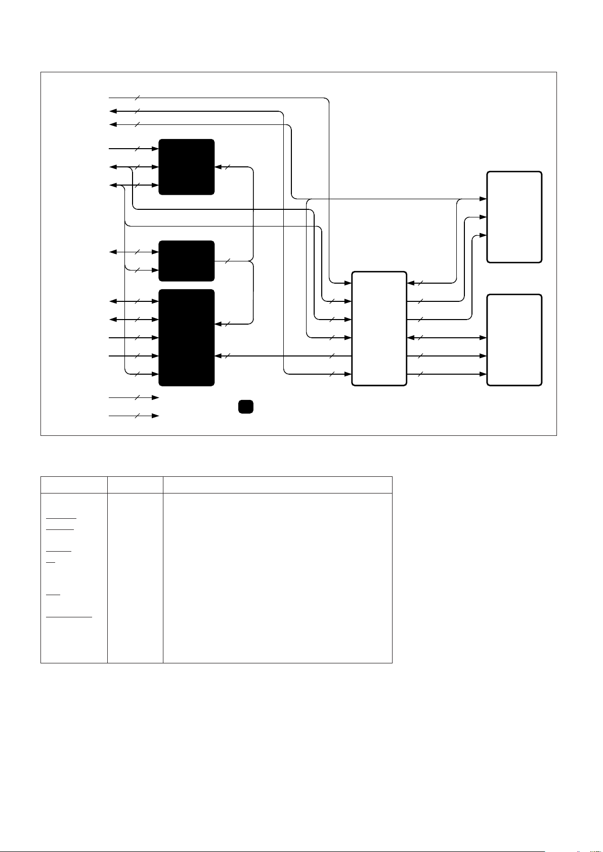
1.0 SYSTEM CONSIDERATIONS
The MA17502 Control Unit (CU) is a component of the
Dynex Semiconductor MAS281 chip set. The other chips in the
set are the MA17501 Execution Unit (EU) and the MA17503
lnterrupt Unit (lU). Also available is the peripheral MA31751
Memory Management Unit/Block Protection Unit (MMU(BPU)).
The Control Unit, in conjunction with these chips, implements
the full MIL-STD-1750A lnstruction Set Architecture. Figure 1
depicts the relationship between the chip set components.
The CU provides the microprogram storage and
sequencing resources for the chip set. The EU provides the
MAS281’s system synchronizing and arithmetic/logic
computational resources. The lU provides interrupt and fault
handling resources, DMA interface control signals, and the
three MIL-STD-1750A timers. The MMU/BPU may be
configured to provide 1M-word memory management (MMU)
and/or 1K-word memory block write protection (BPU) functions.
MA17502
Radiation Hard MIL-STD-1750A Control Unit
Replaces June 1999 version, DS3565-4.0 DS3565-5.0 January 2000
Page 2
MA17502
2/30
Figure 1: MAS281 Chip Set With Optional MA17504 and Support RAMs
Signature l/O Definition
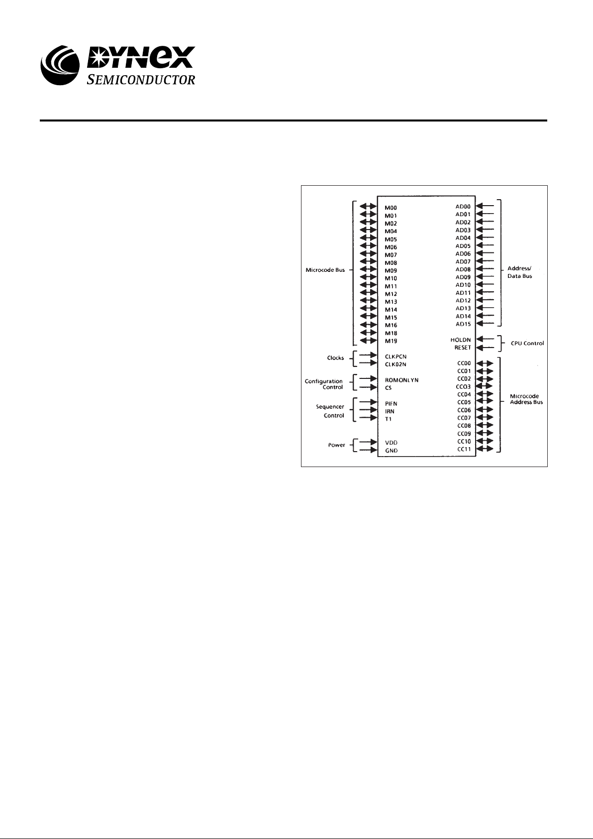
AD00 - AD15 I External 16-Bit Address/Data Bus
CC00 - CC11 I/O 12-Bit Microcode Address Bus
CLKPC I Precharge Clock
CLK02 I Phase 2 Clock
CS I Chip Select
HOLD I Hold Request Suspends lnternal Processor Functions
IR I Interrupt Request
M00 - M19 I/O/Z 20-Bit Microcode Bus
NC - No Connection
PIF I Privileged lnstruction Fault
RESET I Rest Indicates Device Initialization
ROMONLY I Indicates if Control Unit to be Used as ROM Only
T1 I Branch or Jump Control
VDD Power (External), 5 Volts
GND Ground
Table 1: Signal Definitions
MA17501
Execution
Unit
MA17502
Control
Unit
MA17503
Interrupt
Unit
MA31751
Block
Protection
& Memory
Management
Unit
Protection
RAM
128 x 16
Page
RAM
512 x 13
Address
7
Control
1
Data
16
Address
9
Control
1
Data
13
4
3
8
7
16
3
3
20
20
M Bus
16
4
4
7
9
10
1
16
1
16
10
1
8
4
8
Status
Control
Physical Page
Address
Clock
Control
Address/Data
Bus
Control
Control
Faults
Interrupts
Timer
Controls
Power
Reset
MAS281 Chip Set
Page 3

MA17502
3/30
As shown in Figure 1, the MAS281 is the minimum
processor configuration consisting of an Execution Unit, a
Control Unit, and an Interrupt Unit. This configuration is
capable of accessing a 64K-word address space. Addition of
an MMU configured MA31751 allows access to a 1M-word
address space. This can also be configured as a BPU to
provide hardware support for 1K-word memory block write
protection.
The CU, as with all components of the MAS281 chip set, is
fabricated with CMOS/SOS process technology. Input and
output buffers associated with signals external to the MAS281
are TTL compatible.
Detailed descriptions of the CU’s companion chips are
provided in separate data sheets. Additional discussions on
chip set system considerations, interconnection details, and the
Digital Avionics lnstruction Set (DAlS) mix benchmarking
analysis are provided in separate applications notes.
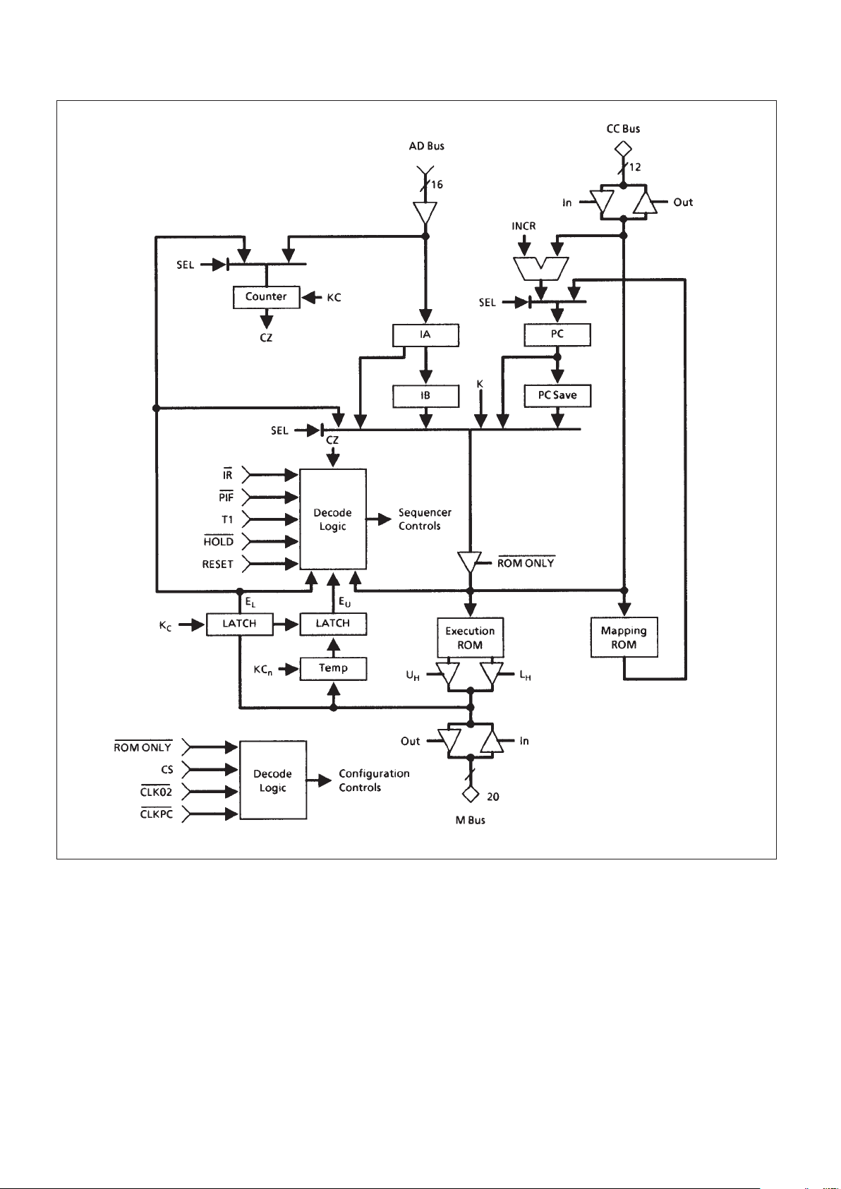
2.0 ARCHITECTURE
The Control Unit consists of a microsequencer, an
instruction mapping ROM, a microcode storage ROM, and
various buses. Details of these components are shown in
Figure 2 and are discussed below:
2.1 MICROSEQUENCER
The CU microsequencer is a 12-bit wide microcode address
generator. Major features of the microsequencer include a
microprogram counter (PC), a microprogram counter save
register (PC Save), microcode address increment logic,
instruction pipeline registers IA and IB, an iteration of loop
counter, a next microcode address source multiplexer, and
various pipelining latches. These features are represented in
Figure 2.
The 12-bit microcode address width allows the
microsequencer to access up to 4096 words of microcode. The
MIL-STD-1750A instructions are implemented as sequences of
microinstructions stored within the lower 2048 locations of this
address space. The address for each microinstruction in a
sequence is provided by the next microcode address source
multiplexer. This multiplexer, under control of the CU control
logic, select from one of six next address sources. Sequential,
direct jump, conditional jump, and subroutine address
generation modes are supported.
Sequential addressing is accomplished by providing a path
from the output of the next microcode address multiplexer to an
incrementer and back to the PC register input. Direct jumps are
supported by routing a portion of the microinstruction to one of
the next microcode address source multiplexer inputs.
Conditional jumps are determined in the ALU of the Execution
Unit which communicates the decision to the CU via the T1
signal. The T1 signal enables a portion of the microcode word
to create the new address. Subroutine jumps are accomplished
by loading the contents of the incremented PC register into the
PC Save register and then performing a direct jump. Upon
completion of the subroutine, the contents of the PC Save
register are used as the next microcode address.
A new microinstruction sequence begins when an opcode
residing in the lA or IB register is selected by the next
microcode address source multiplexer and used as an address
to simultaneously access both the CU’s Instruction Mapping
ROM and the Microcode Storage ROM. The instruction
Mapping ROM access provides a pointer which is then used to
update the microprogram counter (PC); the Microcode Storage
ROM access provides the first microinstruction of the
sequence. Remaining microinstructions in a sequence are
accessed through the use of the four address generation
modes discussed above.
Iterative microprogram operations are achieved through the
use of the loop counter. The loop counter may be selectively
loaded from either the AD bus or directly from microcode. This
counter tracks the number of iterations remaining and, when
appropriate, issues a completion signal (CZ). When an iterative
operation is called for, the loop counter is loaded and the CU
control logic repeats a particular microinstruction sequence,
using the four address generation modes discussed above,
until the CZ signal is received.
2.2 INSTRUCTION MAPPING ROM
The CU instruction mapping ROM provides 512 8-bit words
of microcode instruction vector storage. The address space of
this ROM is mapped into a portion of the microcode storage
ROM’s address space. Hence, both ROMs are accessed
whenever the microcode address falls within this range. The
eight bits from the instruction mapping ROM serve as-the lower
eight bits of a 12-bit microcode address; the upper four bits are
a hardwired constant. The 12-bit microcode address formed
from the 4-bit constant and the mapping ROM’s eight bits are
loaded into the PC register of the microsequencer and serve as
a means to access nonsequential microcode addresses within
the address space allocated to both the instruction mapping
and microcode storage ROMs.
2.3 MICROCODE ROM
The CU microcode ROM provides 2K (2048) 40-bit words of
storage capacity. All of the microcode required to implement
the full MIL-STD-1750A lnstruction Set Architecture (lSA) fits in
one such ROM.
2.4 BUSES
A 16-bit multiplexed Address/Data (AD) bus provides a
communications path between the CU, the other components
of the MAS281 chip set, the MA31751 MMU/BPU, and any
other devices mapped into the chip set’s address space. The
CU receives MIL-STD-1750A instructions, accessed from
system memory, over this bus and loads them into its
instruction pipeline registers.
A 20-bit multiplexed Microcode (M) bus provides a pathway
between the CU chip and the microcode decode logic on all
other chips which are under CU microcode control. The 40-bit
wide microinstructions from the CU’s microcode ROM are
multiplexed on chip as two 20-bit words and presented on the
interchip M bus during alternate phases of CLK02N. Microcode
bits 39 through 20 are placed on the M bus during the CLK02N
low phase and bits 19 through 0 during the high phase of
CLK02N. The M bus is bidirectional to permit microcode
memory expansion.
A 12-bit microcode address (CC) bus is used to route
microcode addresses from the next microcode address source
multiplexer to the microcode and instruction mapping ROMs as
shown in Figure 2.
Page 4

MA17502
4/30
3.0 INTERFACE SIGNALS
All signal definitions are shown in Table 1. In addition, each
of these functions is provided with Electrostatic Discharge
(ESD) protection diodes. All unused inputs must be held to their
inactive state via a connection to VDD or GND.
Throughout this data sheet, active low signals are denoted
by either a bar over the signal name or by following the name
with an “N” suffix. e.g. HOLDN. Referenced signals that are not
found on the MA17502 are preceded by the originating chip’s
functional acronym in parentheses, e.g. (IU)DMAKN.
A description of each pin function, grouped according to
functional interface, follows. The function acronym is presented
first, followed by its definition, its type, and its detailed
description. Function type is either input, output, high
impedance (Hi-Z), or a combination thereof. Timing
characteristics of each of the functions described are provided
in Section 6.0.
3.1 POWER INTERFACE
The power interface consists of a single 5V VDD connection
and two common GND connections.
3.2 CLOCKS
The clock interface, discussed below, is the means by
which the synchronous, microcoded operation of the MAS281
is driven.
3.2.1 Precharge Clock (CLKPCN)
Input. The MA17501 Execution Unit (EU), generates the
CLKPCN signal for the Control Unit. The Control Unit uses this
signal for most of its internal sequencing. During the low phase
of CLKPCN, the internal M Bus is precharged to the high state
to accelerate its response.
The normal CLKPCN period is defined by five OSC cycles
(two cycles low and three cycles high). When a microcode
branch is indicated by the EU, the low state of CLKPCN is
extended to three OSC cycles. During execution of Interrupt
Unit decoded XlO and microcode commands, the high state of
CLKPCN is extended to four OSC cycles. Also, during external
bus cycles, RDYN may be used to cause the EU to prolong the
high state of CLKPCN to greater than three OSC cycles; this
allows the MAS281 chip set to interface with slower external
memory or input/output devices.
During DMA ((IU)DMAKN is low) or Hold ((EU)HLDAKN is
low), CLKPCN will remain low until the CPU takes control
again.
3.2.2 Phase 2 Clock (CLK02N)
Input. The MA17501 generates the CLK02N signal for the
Control Unit. The CU then uses this signal, in conjunction with
CLKPCN, to control the distribution of microcode on the M Bus.
CLK02N is used to multiplex the 40-bit microcode instruction
into two 20-bit words (µW1 and µW2). The high-to-low edge of
CLK02N switches µW1 (bits 39 through 20) off the M Bus while
switching µW2 (bits 19 through 0) onto the M Bus.
The normal CLK02N period is defined by five OSC cycles
(one cycle low, three cycles high, one cycle low). When a
microcode branch is indicated by the EU, the high state of
CLK02N is extended to four cycles. During execution of
Interrupt Unit decoded XIO and microcode commands, the
trailing low state of CLK02N is extended to two OSC cycles.
Also, during external bus cycles, RDYN may be used to cause
the EU to prolong the CLK02N trailing low state to greater than
one OSC cycle; this allows the MAS281 chip set to interface
with slower external memory or inpuVoutput devices.
During DMA ((IU)DMAKN is low) or Hold ((EU)HLDAKN is
low), CLKPCN will remain low until the CPU takes control
again.
3.3 BUSES
The following is a discussion of the communication buses
connecting the three-chip set. The AD Bus and M Bus are
mainly operand transfer buses, while the CC Bus is strictly for
providing microcode addresses to auxiliary CUs.
3.3.1 Address/Data Bus (AD Bus)
Input. These signals comprise the multiplexed address and
data bus. During external bus operations, the AD bus
accommodates the transfer of instructions, from memory and
l/O ports, to the MA17502. During internal bus operations, the
AD bus provides additional data to the Control Unit from the
Execution Unit. AD00 is the most significant bit position and
AD15 is the least significant bit position of both the 16-bit data
and 16-bit address. A high on this bus corresponds to a logic 1
and a low corresponds to a logic 0. lnformation on the AD Bus is
clocked into the CU by the high-to-low transition of CLKPCN.
3.3.2 Microcode Bus (M Bus)
Input/Output/Hi-z. The M Bus is the 20-bit multiplexed
microcode bus. The 40-bit microcode instruction is multiplexed
onto the M Bus as two 20-bit words (µW1 and µW2). The first
half of the microcode word, µW1 (bits 39 through 20), is
assured valid on the high-to-low transition of CLK02N and µW2
(bits 19 through 0) is assured valid on the high-to-low transition
of CLKPCN. M00 corresponds to microcode bit 0 (µW1) or 20
(µW2) while M19 corresponds to microcode bit 19 (µW1) or 39
(µW2). A high level indicates a logic 1 and a low level indicates
a logic 0. A high level on CS allows the Control Unit to distribute
microcode over this bus, a low level places the bus in the high
impedance state.
During DMA or Hold states, CLKPCN is held low, thus
holding the internal M bus in the precharged state. Precharging
the internal M Bus forces the 20 bits of the external M Bus low.
3.3.3 Microcode Address Bus (CC Bus)
Input/Output/Hi-Z. The CC bus is provided for future
expansion and is left unconnected.
3.4 SEQUENCER CONTROL
The following is a discussion of the microsequencer control
input signals. These signals support chip set functions that
require microcode branching based on the results of operations
performed in the Execution or Interrupt Units.
3.4.1 Interrupt Request (IRN)
Input. A low on this input directs the CU to service pending
interrupt requests latched by the Interrupt Unit (IU). Upon
completion of the currently executing MIL-STD-1750A
instruction, the CU checks the IRN input. If IRN is low, then the
CU sequencer will branch to the microcoded interrupt service
routine; else the next MIL-STD-1750A instruction is mapped to
its microcode routine. The microcoded interrupt service routine
Page 5
MA17502
5/30
Figure 2: MA17502 Control Unit Architecture
Page 6

MA17502
6/30
stores the processor state, retrieves the highest priority
pending interrupt’s service routine processor state, and vectors
software execution to the user’s interrupt service routine. IRN
originates in the IU.
3.4.2 Privileged Instruction Fault (PIFN)
A low on this signal causes the CU to enable control of the
DMA interface (located in the Interrupt Unit), abort the currently
executing MIL-STD-1750A instruction and check the IRN input
for a pending level 1 interrupt caused by the IU latching a
memory protect (MPROEN), memory address (EXADEN), or
Bus Time-out fault. PIFN originates in the IU.
3.4.3 Branch or Jump Control (T1)
Input. A high on this input directs the CU microcode address
sequencer to branch execution to a nonsequential microcode
address. This signal is under the control of the Execution Unit’s
ALU and its level is dependent on the outcome of the presently
executing microcode instruction, e.g. conditional branch. T1
originates in the EU.
3.5 CONFIGURATION CONTROL
The following inputs are provided for control of multiple CU
systems. They allow for expansion of the microcode store to 4K
40-bit words.
3.5.1 ROM-Only (ROMONLYN)
Input. This signal is provided for future microcode
expansion and must be pulled up to VDD.
3.5.2 Chip Select (CS)
Input. A high on this signal enables the CU to drive the 20bit external M Bus. This signal is provided for future microcode
expansion and must be pulled up to VDD.
3.6 CPU CONTROL
Grouped under this heading are signals that have CPUwide control of normal operation. Each of these has the ability
to “freeze” the processor.
3.6.1 Hold Request (HOLDN)
Input. A low on this input will suspend internal processor
functions at the end of the currently executing MlL-STD1750A
instruction. When this signal becomes active, the CU
completes the currently executing MIL-STD-1750A instruction,
then branches to the Hold microcode routine and enters the
Hold state. The CU will resume normal operation by refilling the
instruction pipeline registers (IA and IB) upon release of
HOLDN.
3.6.2 System Reset (RESET)
Input. A high on this input for a duration of at least one
CLKPCN period will reset the MAS281 chip set by forcing the
Control Unit to microcode address zero. The high-to-low
transition of this input will cause the CU to begin executing the
MAS281 initialisation sequence starting with the first instruction
in microcode. Built-in Test (BIT) is performed as part of the
initialisation sequence. At the conclusion of initialisation and
successful execution of BIT, the MAS281 will be initialised as
shown in Table 3.
4.0 OPERATING MODES
The following discussions detail the MAS281 chip set
operating modes from the perspective of the Control Unit.
MAS281 operating modes involving the MA17502 include: (1)
Initialisation, (2) lnstruction Execution, (3) Interrupt Servicing,
(4) DMA Support, and (5) HOLD Support.
4.1 INITIALISATION
The MA17502 sequences the MAS281 chip set through the
microcoded initialisation routine in response to a high pulse on
the RESET input. This routine clears the chip set registers,
disables and masks interrupts’ reads the configuration register,
resets the output discrete register (if applicable), initialises the
MMU and BPU (if applicable), performs Built-in Test (BIT),
raises the StartUp ROM Enable discrete, clears and starts
timers A and B, resets the Trigger-Go counter, and loads the
instruction pipeline. The initialisation sequence is contained in
the first 33 locations of microcode ROM (an additional 14
locations contain the optional MMU and BPU initialisation
code). Because the initialisation sequence clears the Execution
Unit’s lnstruction Counter and Status Word (also the address
and processor state copies stored in the MMU(BPU), if
applicable), program execution begins with the instruction
located at address zero (page zero). Table 2 provides a
detailed breakdown of the initialisation sequence and Table 3
summarises the resulting initialised state.
BIT occupies 332 words of microcode storage ROM, and
consists of five subroutines that exercise the internal circuitry of
the MAS281, as outlined in Table 4. BIT begins by pulling the
Normal Power-UP ((IU)NPU) output low; this is the first time
after power-up that the state of NPU is guaranteed. If all five
BIT subroutines execute successfully, NPU is raised high.
If any part of BIT fails, an error code identifying the failed
subroutine is loaded into the Interrupt Unit Fault Register (via
the AD Bus), BlT is aborted, and NPU is left in the low state.
Table 4 defines the coding of the BIT results. (NPU is raised
high through microcode control of the lU in conjunction with the
(EU)lNTREN signal. The BIT error codes are loaded in the lU
Fault Register via the AD Bus under microcode control of the lU
in conjunction with the (EU)lNTREN signal.)
ln the event of such a failure, the resulting chip set reset
state is dependent on where in BIT the error occurred and may
not be the same as that shown in Table 3. A BIT failure
indication in the fault register sets the level 1 pending interrupt.
Since initialisation disables and masks interrupts, the IRN input
will remain high; thus the interrupt will not be serviced
immediately.
The last action performed by the initialisation routine is to
load the instruction pipeline. lnstruction fetches start at memory
location zero (page zero) from the Start-Up ROM (if
implemented). Whether BlT passes or not, the processor will
begin instruction execution at this point.
Note: To complete initialisation and pass BIT, interrupt and
fault inputs must be high for the duration of the initialisation
routine. Also, the Timers A and B must be clocked for BIT
success.
Page 7

MA17502
7/30
Label Cycle
MAIN B1 1. Enable Control of DMAE Output signal
P2.B1 3. Clear MAS281 Execution Unit Status Word (SW)
Clear Interrupt Mask (MK) (Internal l/O command, SKM, 2000H)
B1 4. Clear Pending lnterrupt Register (Pl) and Fault Register (FT) (lnternal l/O Command, CLlR, 2001H)
Clear Instruction Counter (IC)
P5.B1 6. Disable Interrupts (Internal l/O Command, DSBL, 2003H)
P7.B1 8. Clear MMU Status Word (lnternal l/O Command, WSW, 200EH) (Note 1)
P9.B1 10. Disable DMA Access (Internal l/O Command, DMAD, 4007H)
P 11. B1 12. Read Configuration Register (Internal l/O Command, RCW, 8400H, CONFWN Drops low per Figure
25, Section 5.0)
P 13. P 14. B2 15. - (If Output Discrete Register Present, then Continue; Else, Skip to 18)
P (16). I/O (17). Clear Output Discrete Register (External l/O Command)
B2 19. - (If BPU present, then Branch to BPU; else, continue)
P 20. B2 21. - (If MMU present, then Branch to MMU; Else, Continue)
P 22. - (Setup Temporary Register to indicate No MMU Present)
B2 23. - (Branch to MAS281 BIT)
P 24. B1 25. Enable Start-Up ROM (Internal l/O Command, ESUR, 4004H; SURE Raises High per Figure 25,
Section 5.0)
P 26. B1 27. Clear and Start Timer A (Internal l/O Command, OTA, 400AH)
B1 28. Reset the Trigger-Go timer (Internal l/O Command, GO, 400BH)
P 29. B1 30. Clear and Start Tlmer B (Internal l/O Command, OTB, 400EH)
B2 31. - (Branch to Load Instruction Pipeline Routine)
M 32. Load data-ln register (Dl) and instruction Register A (IA) from [IC], Increment IC
M 33. Load Data-ln Register (Dl) and lnstruction Register a (lA) from [lC] ([lA] Moves to lB), lncrement lC
Map Instruction Register B (IB) into Microcode Routine
BPU P (1). -
P (2). - (Set Loop to Clear Memory Protect RAM)
I/O (3). Clear a Location in MPRAM (Internal l/O Command, LMP, 50XXH), Increment Address; Do 128 Times
(4). - (Branch Back to 20.)
MMU P (1). -
P (2). P (3). - (Setup Loop to Load Instruction Page Registers (IPR) and Operand Page Registers (OPR) wlth
Sequential Values of 0 to 255)
P (4). P (5). I/O (6). Load a Location in the IPR with the value of the Locatron Address (Internal l/O Command, WIPR,
51XYH)
I/O (7). Load a Location in the OPR Increment Loaded Value with the Value of the Location Address (Internal
I/O Command, WOPR, 52XYH)
P (8). - (Increment IPR Address)
P (9). - (Increment OPR Address - Repeat Loop [4. - 9.] 256 Times)
B2 (10). - (Setup Temporary Register to Indicate MMU Present; Branch back to 23)
Notes: 1. This operation Is performed whether or not an MMU is present.
2. “-” indicates internal CPU operation.
3. Sequence numbers in “( )” are performed only under the stated conditions.
4. Each step enumerated above represents a single machine (SYNC) cycle of the type shown in the “Cycle” column.
“P” indicates a 5 OSC cycle, 60% duty cycle, machine cycle.
“I/O” and “M” indicate a 5 OSC cycle, 50% duty cycle, machine cycle.
“B1” indicates a 6 OSC cycle 50% duty cycle machine cycle.
“B2” indicates a 6 OSC cycle 66% duty cycle machlne cycle.
Table 2: MAS281 Initialisation Sequence
Page 8

MA17502
8/30
MAS281
Instruction Counter (IC) Zeroed
Status Word (EU and MMU) (SW) Zeroed
Fault (FT) Zeroed
Pending Interrupt (Pl) Zeroed
Mask (MK) Zeroed
General Register File (RO R15) Zeroed
Interrupts Disabled
DMA Access Disabled
TimerA Reset and Started
Timer B Reset and Started
Trigger-Go Timer Reset and Started
MMU
Page Registers Group Zero Enabled
AL, W, E, Fields Zeroed
PPA Field Logical to Physical
Map
BPU
Write Protect Zeroed
Global Memory Protect Enabled
BIT Test BIT Fail Codes Cycles
Coverage (FT
13, 14,15
)
Microcode Sequencer
1 IB Register Control 100 221
Barrel Shifter
Byte Operations and
Flags
Temporary Registers
(T0 - T7)
2 Microcode Flags 101 166
Multiply
Divide
Interrupt Unit
3 MK, Pl, FT 111 214
Enable/Disable
Interrupts
Status Word Control
4 User Flags 110 154
General Registers
(R0 - R15)
5 Timer A 111 763
Timer B
BIT Pass/Fail - 26
Overhead
Note: BIT pass is indicated by all zeros in FT bits 13, 14 and 15
Table 3: Initialisation State
Table 4: Built In Test (BIT) Summary
driven low during execution of this instruction). Interrupt, DMA,
and Hold support are explained in more detail in following
sections.
4.3 DIRECT MEMORY ACCESS
Direct Memory Access (DMA) is controlled by the Execution
Unit (EU) in concert with the Interrupt Unit DMA interface. The
CU supports DMA by suspending processor control upon
completion of the current machine cycle. If DMA is enabled
((UI)DMAE signal, high) a DMA request ((IU)DMARN input,
low) to the MAS281 causes the lU to acknowledge with
DMAKN, low. When the EU receives the DMAKN (DMA
Acknowledge) signal from the lU, the CU clocks are suspended
(CLKPCN, low; CLK02N, high) halting the MAS281’s
microcode sequencing. Microinstruction execution remains
suspended until DMARN is removed. When DMARN is
removed, microcode execution resumes where DMARN had
interrupted it.
4.4 INTERRUPT HANDLING
Interrupts are handled by the interrupt Unit (IU) and
communicated to the CU via the lRN input. The CU checks the
status of the lRN (lnterrupt Request) signal after the completion
of each MlL-STD-1750A microcode instruction sequence. lf the
lRN signal is low, the CU initiates interrupt handling, otherwise
the CU processes a new instruction.
4.2 INSTRUCTION EXECUTION
The MIL-STD-1750A microcoded instruction subroutines
are stored in 1255 locations of microcode storage ROM. The
Control Unit receives instructions from memory, via the AD
Bus, through the instruction pipeline registers lA and IB. When
the previous instruction or special process (Interrupts or Hold)
has been completed, the new instruction residing in register IB
is selected by the next microcode address source multiplexer.
A 4-bit hardwired constant, appended by the instruction
opcode, is then used as the first address of a microcode
sequence which distributes the required control to execute the
instruction. The microsequencer generates the remaining
microcode addresses necessary to complete the sequence as
described in Section 2.0 of this data sheet entitled,
“Architecture”.
Upon completion of the current instruction, the CU will
accept the next instruction in the program unless an interrupt,
DMA, or Hold request is received. The interrupt and Hold
request share a common branch point in microcode. If an
interrupt and Hold request are both pending at the conclusion of
the MIL-STD-1750A instruction microcode routine, the Hold
request has priority and is serviced first. Upon release of the
Hold state, the first instruction will execute even if the interrupt
is still pending; when this instruction is complete the interrupt
will be serviced (assuming the HOLDN input has not been
Page 9
MA17502
9/30
IU interrupt handling is controlled by the CU through three
microcode bits - M04, M05, and M06. Upon receipt of the IRN
signal and after completion of the currently executing
instruction, the CU branches to a microcoded interrupt handling
routine. The microprogram sequence supplies microcoded
control to the lU for reading the highest priority pending
interrupt vector code, which also clears this pending interrupt.
Due to the similarity of interrupt and hold request handling
by the CU, if a Hold and interrupt request are pending at the
end of an instruction sequence the Hold has priority and will be
serviced.
4.5 HOLD SUPPORT
The CU accepts a Hold request in much the same way as
an interrupt request. After the completion of each MlL-STD1750A microcode instruction sequence, the CU checks the
status of the HOLDN signal. If the HOLDN signal is low, a
microcoded sequence suspends further internal processing
functions; otherwise, the CU processes a new instruction or
services interrupt requests (Hold requests have priority over
interrupt requests).
The Control Unit responds to an active HOLDN signal, upon
completion of the currently executing instruction, but branching
to a microprogrammed sequence of instructions that suspends
all internal operations. This sequence of microinstructions
allows the processor to resume instruction execution at the
point HOLDN was accepted when the CU regains control of the
processor. The MAS281 remains in the Hold state until HOLDN
is pulled high (if the Hold state was reached through the
hardware interface, HOLDN) or HOLDN is pulsed low (if the
Hold state was reached through software, BPT instruction).
HOLDN should be synchronised to AS falling.
5.0 SOFTWARE CONSIDERATIONS
The MAS281 chip set implements the full MlL-STD-1750A
instruction set. Table 6a gives a brief listing of this instruction
set and provides performance data for each instruction. Table
6b provides a summary of the l/O commands implemented in
MAS281 and MA31751 MMU/BPU hardware. A complete
description of this instruction set is provided in MIL-STD-1705A
(Notice 1). The register set available to the software
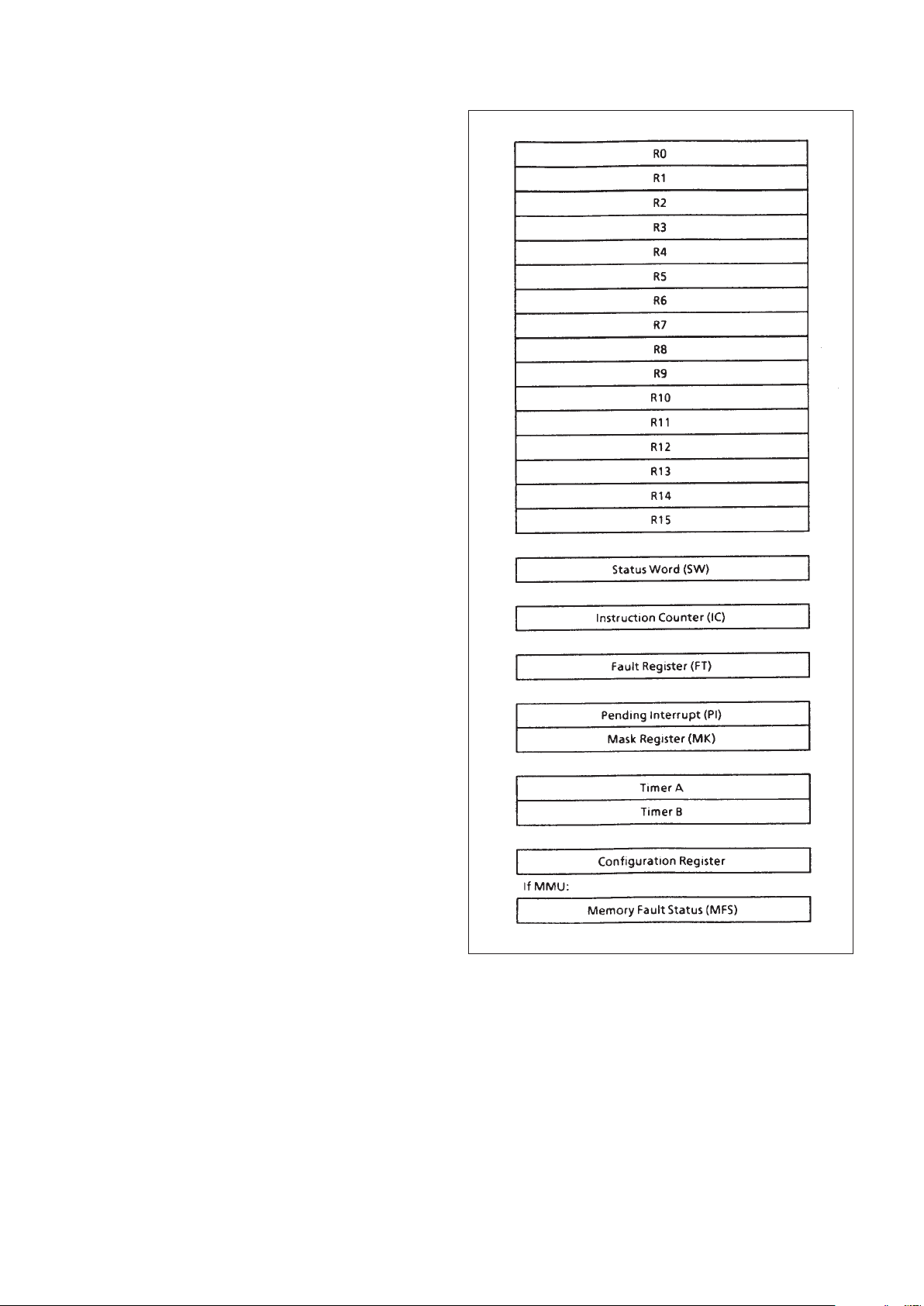
programmer is depicted in Figure 3. A discussion of data types,
addressing modes, and benchmarking considerations fol lows.
5.1 DATA TYPES
The MAS281 chip set supports 16-bit fixed-point single
precision, 32-bit fixed-point double-precision, 32-bit floatingpoint, and 48-bit extended-precision floatingpoint data types.
Figure 4 depicts the formats of these data types.
All numerical data is represented in two’s complement form.
Floating-point numbers are represented by a fractional two’s
complement mantissa with an 8-bit two’s complement
exponent. The MAS281 expects all floating point operands to
be normalised. If they are not normalised, the results from an
instruction are not defined.
Figure 3: Register Set Model
Page 10

MA17502
10/30
5.2 ADDRESSING MODES
The MAS281 chip set supports the eight addressing
modes specified in MIL-STD-1750A. These addressing
modes are shown in Figure 5 and are defined below.
5.2.1 Register Direct (R)
The register specified by the instruction (RB) contains
the required operand.
5.2.2 Memory Direct (D,DX)
Memory Direct (without indexing) is an addressing
mode in which the instruction contains the memory address
(A) of the required operand. ln Memory Direct (indexed),
the memory address of the required operand is specified by
the sum of the contents of an index register (RX) and the
instruction address field (A). Registers R1 through R15
may be specified for indexing.
5.2.3 Memory Indirect (I,IX)
Memory Indirect (without indexing) is an addressing
mode in which the memory address (A) specified by the
instruction contains the address of the required operand. In
Memory Indirect (pre-indexed), the sum of the contents of a
specified index register (RX) and the instruction address
field (A) is the address of the address of the required
operand. Registers R1 through R15 may be specified for
indexing.
5.2.4 Immediate Long (IM)
There are two formats that implement Immediate Long
Addressing; one allows indexing and one does not. For the
indexable format, if the specified index register (RX) is not
equal to zero, the contents of RX are added to the
immediate field to form the required operand, otherwise,
the immediate field contains the required operand .
5.2.5 Immediate Short (IS)
In this mode the required 4-bit operand is contained
within the 16-bit instruction. The Immediate Short
addressing mode accommodates two formats; one which
interprets the contents of the immediate field as positive
data and the other which interprets the contents of the
immediate field as negative data.
5.2.6 Immediate Short Positive (ISP)
The immediate operand is treated as a positive integer
between 1 and 16.
5.2.7 Immediate Short Negative (ISN)
The immediate operand is treated as a negative integer
between 1 and 16. Its internal form is a two’s complement,
sign-extended 16-bit number.
5.2.8 Instruction Counter Relative (ICR)
This addressing mode is used for 16-bit branch
instructions. The contents of the instruction counter minus
two (the address of the current instruction) is added to the
sign-extended 8-bit displacement field (D) within the
instruction. This sum then points to the memory address to
which control may be transferred if a branch is to be taken.
Figure 4: Data Formats
5.2.9 Base Relative (B)
There are two formats which implement Base Relative
Addressing; one allows indexing and one does not. For the nonindexable form the contents of the instruction specified base
register (BR = BR' + 12) is added to the 8-bit displacement field
(DU) of the 16-bit instruction. For the indexable form, the sum of the
contents of a specified index register (RX) and a specified base
register (BR = BR' + 12) is the address of the required operand.
Registers R1 through R15 may be specified for indexing and the
base register may be R12 through R15.
Page 11

MA17502
11/30
Figure 5: Addressing Modes
Page 12

MA17502
12/30
5.2.10 Special (S)
This addressing mode is applicable to instructions that do
not follow the above formats.
5.3 BENCHMARKING
Table 6a defines the number and type of machine cycles
associated with each MIL-STD-1750A instruction. This
information may be used when benchmarking MAS281
performance. The Digital Avionics Instruction Set (DAIS) mix,
which defines a typical frequency of occurrence for MIL-STD1750A instructions, is used here for this purpose.
One problem with the DAlS mix, however, is that it does not
reflect the impact of data dependencies on system
performance. For example, a multiplication in which one
operand is zero may be performed much faster than one with
two non-zero operands. Also, the DAIS mix does not specify
such time consuming operations as normalization and
alignment.
Realistic benchmarks must therefore take both an
instruction mix and data dependencies into account. To this
end, machine cycle counts in Table 6a which have data
dependencies are annotated with either an “a” suffix to reflect
an average number of machine cycles (where each of several
possibilities is equally likely) or with a “wa” suffix to reflect a
weighted average number of machine cycles (where some data
possibilities are more likely than others). Weighted averages
are only applicable to floating-point operations.
Weighted averages provided in Table 6a, based on the
Sweeney (lBM Systems Journal, Vol. 4, No. 1, 1965)
guidelines, take a wide range of data dependencies into
consideration. Normalization and alignment operations are also
represented. Table 5 defines MAS281 throughput, at various
frequencies and wait states, for the DAIS mix using Sweeney
data dependencies.
It should be noted that using the Sweeney guidelines is a
conservative approach to benchmarking. If best case
assumptions are made and such operations as normalization
and alignment are not considered, MAS281 performance
figures are approximately 50% higher than those indicated in
Table 5.
Table 5: Throughput (KIPS)
Page 13

MA17502
13/30
5.4 INSTRUCTION SUMMARY
Cycles*
Operation Op Code/Ext Mnemonic Format M P B
LOAD/STORE
Single Precision Load 81 LR R 1 0 0
0X LB B 2 1 0
4X 0 LBX BX 2 1 0
82 LlSP lSP 1 0 0
83 LlSN ISN 1 0 0
80 L D,DX 3 0 0
85 Ll M IM,IMX 2 0 0
84 Ll I,IX 4 1 0
Double-Precision Load 87 DLR R 1 2 0
0X DLB B 3 1 0
4X 1 DLBX BX 3 2 0
86 D L D,DX 4 0 0
88 DLI I,IX 5 1 0
Single-Precision Store 0X STB B 2 2 0
4X 2 STBX BX 2 2 0
90 ST D,DX 3 1 0
94 STI I,IX 4 1 0
Store a Non-Negative 91 STC D,DX 3 1 0
Constant 92 STCI I,IX 4 1 0
Double-Precision Store 0X DSTB B 3 2 0
4X 3 DSTX BX 3 2 0
96 DST D,DX 4 0 0
98 DSTl I,IX 5 1 0
Load Multiple Registers 89 LM D,DX 3 + n 1 1
Store Multiple Registers 99 STM D,DX 3 + n 1 1
INTEGER ARITHMETIC
Single-Precision lntegerAdd A1 AR R 1 1 0
1X AB B 2 2 0
4X 4 ABX BX 2 2 0
A2 AISP ISP 1 1 0
A0 A D,DX 3 1 0
4A 1 AIM IM 2 1 0
Increment Memory by a A3 INCM D,DX 4 1 0
Positive Integer
Single-Precision Absolute A4 ABS R 1 1.5 1a
Value of Register
Double-Precision Absolute A5 DABS R 1 2.5 1a
Value of Register
* M = memory, P = processor (5 OSC cycles), B = processor (6 OSC cycles), a = average if more than one alternative exists.
Table 6a: Instruction Summary
Page 14

MA17502
14/30
Table 6a (continued): Instruction Summary
Cycles*
Operation Op Code/Ext Mnemonic Format M P B
Double-Precision Integer A7 DAR R 1 3 0
Add A6 DA D,DX 4 1 0
Single Precision Integer B1 SR R 1 1 0
Subtract 1X SBB B 2 2 0
4X 5 SBBX BX 2 2 0
B2 SISP ISP 1 1 0
B0 S D,DX 3 1 0
4A 2 SIM IM 2 1 0
Decrement Memory by a B3 DECM D,DX 4 1 0
Positive Integer
Single Precision Negate B4 NEG R 1 1 0
Register
Double-Precision Negate B5 DNEG R 1 3 0
Register
Double-Precision Integer B7 DSR R 1 3 0
Subtract B6 DS D,DX 4 1 0
Single Precision Integer C1 MSR R 1 6.5 4a
Multiply with 16-Bit Product C2 MISP ISP 1 7.5 4a
C3 MISN ISN 1 7.5 4a
C0 MS D,DX 3 6.5 4a
4A 4 MSIM IM 2 6.5 4a
Single Precision Integer C5 MR R 1 5 3
Multiply with 32-Bit Product 1X MB B 2 7 3
4X 6 MBX BX 2 7 3
C4 M D, DX 3 5 3
4A 3 MIM IM 2 5 3
Double-Precision Integer C7 DMR R 1 41 4.5a
Multiply C6 DM D,DX 4 40 4.5a
D1 DVR R 1 20.25 5.5a
Single Precision Integer D2 DISP ISP 1 20 5.5a
Divide with 16-Bit Dividend D3 DISN ISN 1 20.5 5.5a
D0 DV D,DX 3 20.25 5.5a
4A 6 DVIM IM 2 20.25 5.5a
Single Precision Integer D5 DR R 1 21.75 6.5a
Divide with 32-Bit Dividend 1 X DB R 2 22.75 6.5a
4X 7 DBX BX 2 22.75 6.5a
D4 D D,DX 3 21.75 6.5a
4A 5 DIM IM 2 22.75 6.5a
Double-Precision Integer D7 DDR R 1 79.5 5.5a
Divide D6 DD D,DX 4 77.5 5.5a
* M = memory, P = processor (5 OSC cycles), B = processor (6 OSC cycles), a = average if more than one alternative exists.
Page 15

MA17502
15/30
Table 6a (continued): Instruction Summary
Cycles*
Operation Op Code/Ext Mnemonic Format M P B
LOGICAL
Inclusive Logical OR E1 ORR R 1 0 0
3X ORB B 2 1 0
4X F ORBX BX 2 1 0
E0 OR D,DX 3 0 0
4A 8 ORIM IM 2 0 0
Logical AND E3 ANDR R 1 0 0
3X ANDB B 2 1 0
4X E ANDX BX 2 1 0
E2 AND D,DX 3 0 0
4A 7 ANDM IM 2 0 0
Exclusive Logical OR E5 XORR R 1 0 0
E4 XOR D,DX 3 0 0
4A 9 XORM IM 2 0 0
Logical NAND E7 NR R 1 1 0
E6 N D,DX 3 1 0
4A B NIM IM 2 1 0
Set Bit 51 SBR R 1 0 0
50 SB D,DX 4 1 0
52 SBI I,IX 5 2 0
Reset Bit 54 RBR R 1 1 0
53 RB D,DX 4 1 0
55 RBI I,IX 5 2 0
Test Bit 57 TBR R 1 0 0
56 TB D, DX 3 0 0
58 TBI I,IX 4 1 0
Test and Set Bit 59 TSB D,DX 4 0 2
Set Variable Bit in Register 5A SVBR R 1 0 1
Reset Variable Bit in Register 5C RVBR R 1 1 1
Test Variable Bit in Register 5E TVBR R 1 0 1
Store Register Through Mask 97 SRM D,DX 4 3 0
BYTE
Load From Upper Byte 8B LUB D,DX 3 0 0
8D LUBl I,IX 4 1 0
Load From Lower Byte 8C LLB D,DX 3 1 0
8E LLBI I,IX 4 2 0
Store Into Upper Byte 9B STUB D,DX 4 1 0
9D SUBI I, IX 5 3 0
Store Into Lower Byte 9C STLB D,DX 4 1 0
9E SLBI I,IX 5 2 0
Exchange Bytes in Register EC XBR S 1 0 1
* M = memory, P = processor (5 OSC cycles), B = processor (6 OSC cycles), a = average if more than one alternative exists.
Page 16

MA17502
16/30
Table 6a (continued): Instruction Summary
Cycles*
Operation Op Code/Ext Mnemonic Format M P B
COMPARE
Single-Precision Compare F1 CR R 1 0 0
3X CB B 210
4X C CBX BX 2 1 0
F2 CISP ISP 1 0 0
F3 CISN ISN 1 0 0
F0 C D,DX 3 0 0
4A A CIM IM 2 0 0
Compare Between Limits F4 CBL D,DX 4 2.75 1.75a
Double-Precision Compare F7 DCR R 1 2 0
F6 DC D,DX 4 0 0
JUMP/BRANCH
Jump on Condition 70 JC D,DX 2 0.5 1a
71 JCl I,IX 3 0.5 1a
Jump to Subroutine 72 JS D,DX 2 2 0
Subtract One and Jump 73 SOJ D,DX 2 2.5 1a
Branch Unconditionally 74 BR ICR 2 2 0
Branch if Equal to (zero) 75 BEz ICR 1.5 1 1a
Branch if Less than (zero) 76 BLT ICR 1.5 1 1a
Branch to Executive 77 BEX S 16 12 3a
Branch if Less than or Equal to (Zero) 78 BLE ICR 1.5 1 1a
Branch if Greater than (Zero) 79 BGT ICR 1.5 1 1a
Branch if Not Equal to (Zero) 7A BNZ ICR 1.5 1 1a
Branch if Greater than or Equal to (Zero) 7B BGE ICR 1.5 1 1a
SHIFT
Shift Left Logical 60 SLL R 1 1 0
Shift Right Logical 61 SRL R 1 1 0
Shift Right Arithmetic 62 SRA R 1 1 0
Shift Left Cyclic 63 SLC R 1 1 0
Double Shift Left Logical 65 DSLL R 1 3 0
Double Shift Right Logical 66 DSRL R 1 2 0
Double Shift Right Arithmetic 67 DSRA R 1 2 0
Double Shift Left Cyclic 68 DSLC R 1 3 0
Shift Logical, Count in Register 6A SLR R 1 1 3
Shift Arithmetic, Count in Register 6B SAR R 1 1.5 3.50a
Shift Cyclic, Count in Register 6C SCR R 1 1 3.25a
Double Shift Logical, Count in Register 6D DSLR R 1 2.25 4a
Double Shift Arithmetic, Count in Register 6E DSAR R 1 3.19 4.94a
Double Shift Cyclic, Count in Register 6F DSCR R 1 3.5 3a
* M = memory, P = processor (5 OSC cycles), B = processor (6 OSC cycles), a = average if more than one alternative exists.
Page 17

MA17502
17/30
Cycles*
Operation Op Code/Ext Mnemonic Format M P B
CONVERT
Convert Floating-Point to 16-Bit E8 FIX R 1 4.25 4.5a
Integer
Convert 16-Bit Integer to Floating- E9 FLT R 1 3 2a
Point
Convert Extended-Precision EA EFIX R 1 12.25 6.25a
Floating-Point to 32-Bit lnteger
Convert 32-Bit Integer to EB EFLT R 1 7.5 3.5a
Extended-Precision Floating-Point
STACK
Stack lC and Jump to Subroutine 7E SJS D,DX 4 3 0
Unstack lC and return from
Subroutine 7F URS S 3 1
Pop Multiple registers off the
Stack 8F POPM S 2.5 + n 2.25 + n 4.25a
(n=0-15) (n=0-15)
Push Multiple Registers onto the
Stack 9F PSHM S 1 + n 4.5 + n 2a
(n=0-15) (n=0-15)
I/O (See l/O Command Summary)
Execute l/O 48 XIO** IM,IMX 3 3.583 6.277a
Vectored l/O 49 VIO** D,DX - - -
SPECIAL
Built-ln Function Call 4F BIF S
Move Multiple Words, Memory-to- 93 MOV S 1 + 4n 1 + 3n 1 + 2na
Memory
Exchange Words in Registers ED XWR R 1 2 0
Load Status 7D LST** D,DX 8 2 3
7C LSTI** I,IX 9 2 4
No Operation FF NOP S 1 2 2
Break Point FF BPT S 3 4 4
* M = memory, P = processor (5 OSC cycles), B = processor (6 OSC cycles). ** Privileged instruction.
a = average if more than one alternative exists.
Table 6a (continued): Instruction Summary
Page 18

MA17502
18/30
Cycles*
Operation Op Code/Ext Mnemonic Format M P B
FLOATING-POINT
Extended-Precision Floating- 8A EFL D,DX 5 0 1
Point Load
Extended-Precision Floating- 9A EFST D,DX 5 0 1
Point Store
Floating-Point Absolute Value AC FABS R 1 1 .75 3.25a
of Register
Floating-Point Negate Register BC FNEG R 1 3.25 3.75a
Floating-Point Compare F9 FCR R 1 2.75 2.875wa
3X FCB B 2 2.75 2.875wa
4X D FCBX BX 2 2.75 2.875wa
F8 FC D,DX 3 1.75 2 875wa
Extended-Precision Floating- FB EFCR R 1 3.25 2.875wa
Point Compare FA EFC D,DX 4.25a 2.75 2.875wa
Floating-Point Add A9 FAR R 1 7.625 8.25wa
2X FAB B 3 6.625 8.25wa
4X 8 FABX BX 3 6.625 8.25wa
A8 FA D,DX 4 5.625 8.25wa
Extended-Precision Floating- AB EFAR R 1 21.3125 10.5625wa
Point Add AA EFA D,DX 5 19.3125 10.5625wa
Floating-Point Subtract B9 FSR R 1 8.625 8.625wa
2X FSB B 3 7.625 8.625wa
4X 9 FSBX BX 3 7.625 8.625wa
B8 FS D,DX 4 6.625 8.625wa
Extended-Precision Floating- BB EFSR R 1 23.0625 11.8125wa
Point Subtract BA EFS D,DX 5 21.0625 11.8125wa
Floating-Point Multiply C9 FMR R 1 12.75a 6.25wa
2X FMB B 3 12.75a 6.25wa
4X A FMBX BX 3 12.75a 6.25wa
C8 FM D,DX 4 11.75a 6.25wa
Extended-Precision Floating- CB EFMR R 1 59.75 6.25wa
point Multiply CA EFM D,DX 5 57.75 6.25wa
Floating-Point Divide D9 FDR R 1 31.5 32.75wa
2X FDB B 3 30. 5 32.75wa
4X B FDBX BX 3 30.5 32.75wa
D8 FD D,DX 4 29.5 32.75wa
Extended-Precision Floating- DB EFDR R 1 102.625 47.875wa
Point Divide DA EFD D,DX 5 100.625 47.875wa
* M = memory, P = processor (5 OSC cycles), B = processor (6 OSC cycles), a = average if more than one alternative exists,
wa = weighted average favouring one or more possible alternatives.
Table 6a (continued): Instruction Summary
Page 19

MA17502
19/30
Cycles*
Command
Operation Code (Hex) Mnemonic M P B
Implemented in MAS281
Set Fault Register 0401 SFR 2 3 9
Set Interrupt Mask 2000 SMK 2 3 9
Clear Interrupt request 2001 CLIR 2 3 9
Enable Interrupts 2002 ENBL 2 3 9
Disable Interrupts 2003 DSBL 2 3 9
Reset Pending Interrupt 2004 RPI 2 3 9
Set Pending Interrupt Register 2005 SPI 2 3 9
Reset Normal Power Up Discrete 200A RNS 2 3 9
Write Status Word 200E WSW 2 3a 8.5a
Enable Start-Up ROM 4004 ESUR 2 3 9
Disable Start-Up ROM 4005 DSUR 2 3 9
Direct Memory Access Enable 4006 DMAE 2 3 9
Direct MemoryAccess Disable 4007 DMAD 2 3 9
Ti mer A Start 4008 TAS 2 3 9
Ti mer A Halt 4009 TAH 2 3 9
Output Timer A 400A OTA 2 3 9
Reset Trigger-Go 400B GO 2 3 9
Timer B Start 400C TBS 2 3 9
Timer B Halt 400D TBH 2 3 9
Output Timer B 400E OTB 2 3 9
Read Configuration Word 8400 RCW 2 2 4
Read Fault Register Without Clear 8401 RFR 2 2 4
Read Interrupt Mask A000 RMK 2 2 4
Read Pending Interrupt Register A004 RPIR 2 2 4
Read Status Word A00E RSW 2 1 4
Read and Clear Fault Register A00F RCFR 2 2 4
Input Timer A C00A ITA 2 2 4
Input Timer B C00E ITB 2 2 4
Implemented in BPU
Memory Protect Enable 4003 MPEN 2 4 8
Load Memory Protect RAM 50XX LMP 2 4 8
Read Memory Protect RAM D0XX RMP 2 3 3
Implemented in MMU
Write Instruction Page Register 51XY WIPR 2 4 8
Write Operand Page Register 52XY WOPR 2 4 8
Read Memory Fault Status A00D RMFS 2 3 3
Read Instruction Page Register D1XY RIPR 2 3 3
Read Operand Page Register D2XY ROPR 2 3 3
* M = memory, P = processor (5 OSC cycles), B = processor (6 OSC cycles), a = average if more than one
alternative exists.
5.5 INTERNAL I/O COMMAND SUMMARY
Table 6b: Internal I/O Command Summary
Page 20

MA17502
20/30
6.0 TIMING CHARACTERISTICS
This section provides the detailed timing specifications for
the MA17502. Figure 6 depicts the test load used to obtain
timing data. Figures 7 through 9 depict the timing waveforms
associated with various MA17502 signals. Table 7 provides
values for parameters specified in the timing waveforms. All
timing values provided in Table 7 are valid over the full military
temperature range (-55°C to +125°C), and are measured from
50% point to 50% point (50% of VDD supply voltage, unless
otherwise specified). Crosshatching in Figure 7 indicates either
a “don’t care” or indeterminate state.
Figure 6: Test Load
Subgroup Definition
1 Static characteristics specified in Table 9 at +25°C
2 Static characteristics specified in Table 9 at +125°C
3 Static characteristics specified in Table 9 at -55°C
7 Functional tests at +25°C
8a Functional tests at +125°C
8b Functional tests at -55°C
9 Switching characteristics specified in Table 7b at +25°C
10 Switching characteristics specified in Table 7b at +125°C
11 Switching characteristics specified in Table 7b at -55°C
Table 7a: Definition of Subgroups
No. Parameter Test Condition
(1) (2)
Min Max Units
1 CLKPC ↑ to Microword 1 Valid Load 1 - 95 ns
2 CLK02 ↓ to Microword 2 Valid Load 1 - 41 ns
3 Microword 1 after CLK02 ↓ Load 1 5 - ns
4 Microword 2 after CLKPC ↓ Load 1 25 - ns
5 AD Bus to CLKPC ↓ -10 -ns
6 T1 to CLKPC ↑ -20 -ns
7 PIF to CLKPC ↑ -20 -ns
8 IR to CLKPC ↑ -20 -ns
9 HOLD to CLKPC ↓ -15 -ns
10 RESET to CLKPC ↓ -15 -ns
11 AD Bus after CLKPC ↓ -15 -ns
12 HOLD after CLKPC ↓ -15 -ns
13 RESET after CLKPC ↓ -15 -ns
14 T1, PlF, lR after CLKPC ↓ -0-ns
Mil-Std-883, Method 5005, Subgroup 9, 10, 11
Notes: 1. TA = +25°C, -55°C and +125°C tested at VDD = 4.5V and 5.5V.
2. Unless otherwise noted: VIL ≥ 0.0V, VIHTTL ≤ 4.0V; timing measured from 50% to 50% point.
Table 7b: Timing Parameter Values
Page 21

MA17502
21/30
Figure 7: Basic Timing
Figure 9:
HOLD
Timing
Figure 8: RESET Timing
Page 22

MA17502
22/30
Table 8: Absolute Maximum Ratings
7.0 ABSOLUTE MAXIMUM RATINGS
Parameter Min Max Units
Supply Voltage -0.5 7 V
Input Voltage -0.3 VDD+0.3 V
Current Through Any Pin -20 +20 mA
Operating Temperature -55 125 °C
Storage Temperature -65 150 °C
Note: Stresses above those listed may cause permanent
damage to the device. This is a stress rating only and
functional operation of the device at these conditions, or at
any other condition above those indicated in the operations
section of this specification, is not implied. Exposure to
absolute maximum rating conditions for extended periods
may affect device reliability.
Total Dose Radiation Not
Exceeding 3x10⁵ Rad(Si)
Symbol Parameter Conditions Min Typ Max Units
V
DD
Supply Voltage VSS = 0 4.5 5.0 5.5 V
V
IHC
CMOS Input High Voltage (Note 1) - VDD-1 - - V
V
ILC
CMOS Input Low Voltage (Note 1) - - - VSS+1 V
V
IHT
TTL Input High Voltage (Note 2) - 2.0 - - V
V
ILT
TTL Input Low Voltage (Note 2) - - - 0.8 V
V
OHC
CMOS Output High Voltage (Note 1) IOH = -1.4mA, VDD = 4.5V 4.0 - - V
V
OLC
CMOS Output Low Voltage (Note 1) IOL = 2mA, VDD = 5.5V - - 0.5 V
I
IL
Input Leakage Current (Note 3) VDD = 5.5V, VIN = 0V or 5.5V - - ±10 µA
I
OZ
Output Leakage Current (Note 3) VDD = 5.5V, VO = 0V or 5.5V - - ±50 µA
I
IPU
CS or ROMONLYN Input Pull-up VDD = 5.5V, - - -300 µA
Current (Note 4) CS or ROMONLYN = 0V
I
DDOP
Operating Supply Current VDD = 5.5V, - 25 35 mA
CLKPCN = CLK02N = 4MHz
I
DDST
Static Supply Current VDD = 5.5V, - 5 10 mA
CLKPCN = CLK02N = 0MHz
VDD = 5V±10%, over full operating temperature range.
Mil-Std-883, Method 5005, Subgroup 1, 2, 3
Notes: 1. The following signals are CMOS compatible:
a) CMOS inputs: CS, ROMONLYN, T1, IRN, PIFN, CLK02N and CLKPCN
b) CMOS I/O signals: Microcode bus (M00-M19) and Microcode address bus (CC00-CC11)
2. The following signals are TTL compatible:
a) TTL inputs: Address/Data Bus (AD00-AD15), RESET and HOLDN
3. Worst case at TA = +125°C, guaranteed but not tested at TA = -55°C
4. CS and ROMONLYN inputs are provided for future microcode expansion and have internal pullup resistors. These
signals should be high for normal operation.
8.0 DC ELECTRICAL CHARACTERISTICS
Table 9: DC Electrical Characteristics
Page 23

MA17502
23/30
9.0 PACKAGING INFORMATION
Ref
Millimetres Inches
Min. Nom. Max. Min. Nom. Max.
A - - 5.715 - - 0.225
A1 0.38 - 1.53 0.015 - 0.060
b 0.35 - 0.508 0.014 - 0.020
c 0.229 - 0.36 0.009 - 0.014
D - - 82.04 - - 3.230
e - 2.54 Typ. - - 0.100 Typ. -
e1 - 22.86 Typ. - - 0.900 Typ. -
H 4.71 - 5.38 0.185 - 0.212
Me - - 23.4 - - 0.920
Z - - 1.27 - - 0.050
W - - 1.53 - - 0.060
XG413
D
W
A
e b Z
H
A
1
15°
M
E
C
e
1
Seating Plane
Figure 10a: 64-Pin Ceramic DIL - Package Style C
Page 24

MA17502
24/30
Figure 10b: Pin Assignments
1
IRN
2
VDD
3
PIFN
4
AD00
5
AD01
6
AD02
7
AD03
8
AD04
9
AD05
10
AD06
Top
View
11AD07
12
AD08
13
AD09
14
AD10
15
AD11
16
AD12
17
AD13
18
AD14
19
AD15
20
CLK02N
21
CLKPCN
22
M19
23
M18
24
M17
25
M16
26
M15
27
M14
28
M13
29
M12
30
M11
31
M10
32
M09
64
HOLDN
63
RESET
62
T1
61
NC
60
NC
59
GND
58
NC
57
ROMONLYN
56
CC11
55
CC10
54
CC09
53
CC08
52
CC07
51
CC06
50
CC05
49
CC04
48
CC03
47
CC02
46
CC01
45
CC00
44
M00
43
CS
42
GND
41
M01
40
M02
39
M03
38
M04
37
M05
36
M06
35
M07
34
NC
33
M08
Page 25

MA17502
25/30
Ref
Millimetres Inches
Min. Nom. Max. Min. Nom. Max.
A 1.905 - 2.21 0.075 - 0.087
b1 - 0.51 - - 0.020 -
D 18.08 - 18.62 0.712 - 0.733
E 18.08 - 18.62 0.712 - 0.733
e - 1.02 - - 0.040 Z 1.40 - 1.78 0.055 - 0.070
XG493
Bottom
View
Pad 1
Radius r
3 corners
E
Z
e b
1
D A
Figure 11a: 64-Pad Leadless Chip Carrier - Package Style L
Page 26

MA17502
26/30
Figure 11b: Pin Assignments
Bottom
View
6
5
4
3
2
1
64
63
62
61
60
59
25
26
27
28
29
30
31
32
33
34
35
36
M16
M15
M14
M13
M12
M11
M10
M09
M08
NC
M07
M06
AD02
AD01
AD00
PIFN
VDD
IRN
HOLDN
RESET
T1
NC
NC
GND
20191817161514131211109
AD05
AD06
AD07
AD08
AD09
AD10
AD11
AD12
AD13
AD14
AD15
CLK02N
414243444546474849505152
CC07
CC06
CC05
CC04
CC03
CC02
CC01
CC00
M00
CS
GND
M01
8
7
AD04
AD03
24232221
CLKPCN
M19
M18
M17
37
38
39
40
M05
M04
M03
M02
53545556
CC11
CC10
CC09
CC08
58
57
NC
ROMONLYN
Page 27

MA17502
27/30
Ref
Millimetres Inches
Min. Nom. Max. Min. Nom. Max.
A - - 2.72 - - 0.107
A1 1.83 - 2.24 0.072 - 0.088
b 0.41 - 0.51 0.016 - 0.020
c 0.20 - 0.30 0.008 - 0.012
D1, D2 23.88 - 24.51 0.940 - 0.960
e - 2.54 - - 0.050 j1 - 1.02 - - 0.040 j2 - 0.51 - - 0.020 L 10.16 - 10.54 0.400 - 0.415
Z 1.65 - 2.16 0.065 - 0.085
XG540
Figure 12a: 68-Lead Topbraze Flatpack - Package Style F
Top View
j1
D1L
Pin 1
j2
b
e
D2
Z
A1
A
c
Page 28

MA17502
28/30
Figure 12b: Pin Assignments
Top View
27
26 25 24 23 22 21 20 19 18 17 16 15 14 13 12 11 10
28
29
30
31
32
33
34
35
36
37
38
39
40
41
42
43
9
8
7
6
5
4
3
2
1
68
67
66
65
64
63
62
61
44 45 46 47 48 49 50 51 52 53 54 55 56 57 58 59 60
AD04
AD03
AD02
AD01
AD00
PIFN
VDD
NC
IRN
HOLDN
RESET
T1
NC
NC
NC
GND
NC
M15
M14
M13
M12
M11
M10
M09
M08
NC
NC
M07
M06
M05
M04
M03
M02
M01
M16
M17
M18
M19
CLKPCN
CLK02N
AD15
AD14
AD13
AD12
AD11
AD10
AD09
AD08
AD07
AD06
AD05
NC
GND
CS
M00
CC00
CC01
CC02
CC03
CC04
CC05
CC06
CC07
CC08
CC09
CC10
CC11
ROMONLYN
Page 29

MA17502
29/30
10.0 RADIATION TOLERANCE
Total Dose Radiation Testing
For product procured to guaranteed total dose radiation
levels, each wafer lot will be approved when all sample devices
from each lot pass the total dose radiation test.
The sample devices will be subjected to the total dose
radiation level (Cobalt-60 Source), defined by the ordering
code, and must continue to meet the electrical parameters
specified in the data sheet. Electrical tests, pre and post
irradiation, will be read and recorded.
Dynex Semiconductor can provide radiation testing
compliant with Mil-Std-883 method 1019 Ionizing Radiation
(total dose) test.
11.0 ORDERING INFORMATION
For details of reliability, QA/QC, test and assembly
options, see ‘Manufacturing Capability and Quality
Assurance Standards’ Section 9.
Unique Circuit Designator
S
R
Q
Radiation Hard Processing
100 kRads (Si) Guaranteed
300 kRads (Si) Guaranteed
Radiation Tolerance
C
F
L
Ceramic DIL (Solder Seal)
Flatpack (Solder Seal)
Leadless Chip Carrier
Package Type
QA/QCI Process
(See Section 9 Part 4)
Test Process
(See Section 9 Part 3)
Assembly Process
(See Section 9 Part 2)
L
C
D
E
B
S
Rel 0
Rel 1
Rel 2
Rel 3/4/5/STACK
Class B
Class S
Reliability Level
MAx17502xxxxx
Total Dose (Function to specification)* 3x10⁵ Rad(Si)
Transient Upset (Stored data loss) 1x10
11
Rad(Si)/sec
Transient Upset (Survivability) >1x10¹² Rad(Si)/sec
Neutron Hardness (Function to specification) >1x10¹⁵ n/cm
2
Single Event Upset** <1x10
-10
Errors/bit day
Latch Up Not possible
* Other total dose radiation levels available on request
** Worst case galactic cosmic ray upset - interplanetary/high altitude orbit
Table 10: Radiation Hardness Parameters
Page 30

MA17502
30/30
CUSTOMER SERVICE CENTRES
France, Benelux, Italy and Spain Tel: +33 (0)1 69 18 90 00. Fax: +33 (0)1 64 46 54 50
North America Tel: 011-800-5554-5554. Fax: 011-800-5444-5444
UK, Germany, Scandinavia & Rest Of World Tel: +44 (0)1522 500500. Fax: +44 (0)1522 500020
SALES OFFICES
France, Benelux, Italy and Spain Tel: +33 (0)1 69 18 90 00. Fax: +33 (0)1 64 46 54 50
Germany Tel: 07351 827723
North America Tel: (613) 723-7035. Fax: (613) 723-1518. Toll Free: 1.888.33.DYNEX (39639) /
Tel: (831) 440-1988. Fax: (831) 440-1989 / Tel: (949) 733-3005. Fax: (949) 733-2986.
UK, Germany, Scandinavia & Rest Of W orld Tel: +44 (0)1522 500500. Fax: +44 (0)1522 500020
These offices are supported by Representatives and Distributors in many countries world-wide.
© Dynex Semiconductor 2000 Publication No. DS3565-5 Issue No. 5.0 January 2000
TECHNICAL DOCUMENTATION – NOT FOR RESALE. PRINTED IN UNITED KINGDOM
HEADQUARTERS OPERATIONS
DYNEX SEMICONDUCTOR LTD
Doddington Road, Lincoln.
Lincolnshire. LN6 3LF. United Kingdom.
Tel: 00-44-(0)1522-500500
Fax: 00-44-(0)1522-500550
DYNEX POWER INC.
Unit 7 - 58 Antares Drive,
Nepean, Ontario, Canada K2E 7W6.
Tel: 613.723.7035
Fax: 613.723.1518
Toll Free: 1.888.33.DYNEX (39639)
This publication is issued to provide information only which (unless agreed by the Company in writing) may not be used, applied or reproduced for any purpose nor form part of any order or contract nor to be regarded
as a representation relating to the products or services concerned. No warranty or guarantee express or implied is made regarding the capability, performance or suitability of any product or service. The Company
reserves the right to alter without prior notice the specification, design or price of any product or service. Information concerning possible methods of use is provided as a guide only and does not constitute any guarantee
that such methods of use will be satisfactory in a specific piece of equipment. It is the user's responsibility to fully determine the performance and suitability of any equipment using such information and to ensure
that any publication or data used is up to date and has not been superseded. These products are not suitable for use in any medical products whose failure to perform may result in significant injury
or death to the user. All products and materials are sold and services provided subject to the Company's conditions of sale, which are available on request.
All brand names and product names used in this publication are trademarks, registered trademarks or trade names of their respective owners.
http://www.dynexsemi.com
e-mail: power_solutions@dynexsemi.com
Datasheet Annotations:
Dynex Semiconductor annotate datasheets in the top right hard corner of the front page, to indicate product status. The annotations are as follows:Target Information: This is the most tentative form of information and represents a very preliminary specification. No actual design work on the product has been
started.
Preliminary Information: The product is in design and development. The datasheet represents the product as it is understood but details may change.
Advance Information: The product design is complete and final characterisation for volume production is well in hand.
 Loading...