

Page 1
MA31755
1/13
The MA31755 is a 16 bit Error Detection and Correction
Unit intended for use in high integrity systems for monitoring
and correcting data values retrieved from memory. The EDAC
is placed in the data bus between the processor and the
memory to be protected. Extra check bits added at each
memory location are programmed transparently by the EDAC
during a processor write cycle. The entire checkword and data
combination is verified on read cycles. If any one bit in the
incoming data stream is at fault the EDAC can correct the fault
transparently, presenting the corrected 16-bit value to the
processor. An error in two bits can be detected but cannot be
corrected. Both the correctable and uncorrectable error
conditions are signalled to the system to allow the processor to
take action as required. Parity is passed through the device
unchanged as data bus bit 16.
Tri-statable bus transceivers with a high drive capability
are incorporated at the MD and CB busses which allows the
usual bus driver devices to be removed and reduces the
overall timing overhead imposed on the data bus. Although
designed primarily for MA31750 application, this part may be
used in almost any 16-bit processor system requiring high data
integrity.
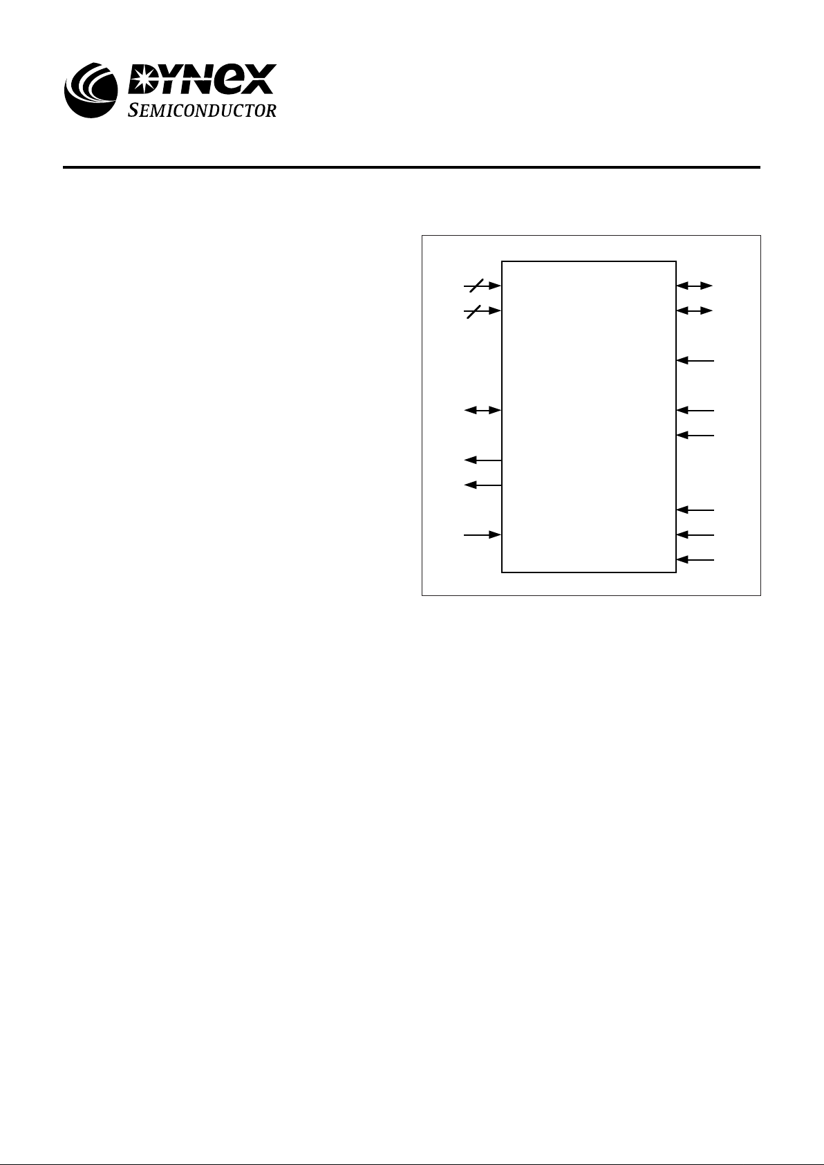
Figure 1: Chip Signals
FEATURES
■ Fast Feedthrough (35ns Detect and Correct Cycle)
■ 16-Bit Operation with 6 Check Bits
■ Radiation Hard CMOS/SOS Technology
■ Feedthrough Operation
■ Error Corrected/Uncorrected Flags
■ High Drive Capability on Memory Busses
VDD
VSS
PD[0:16]
CERRN
NCERRN
RDWN
MD[0:16]
CB[0:5]
XERRN
ENCOR
ENFLG
CS0
CS1N
CS2N
MA31755
EDAC
8
8
MA31755
16-Bit Feedthrough Error Detection
& Correction Unit (EDAC)
Replaces June 1999 version, DS3572-3.0 DS3572-4.0 January 2000
Page 2

MA31755
2/13
1. PIN DESCRIPTIONS
POWER
BUSSES
ERROR FLAGS AND CONTROL
DEVICE AND BUFFER CONTROL
PD[0:16] I/O Active High Processor data bus + parity bit (bit 16)
MD[0:16] I/O Active High Memory data bus + parity bit (bit 16)
CB[0:5] I/O Active High Memory check bit bus
VDD x8 Input - Supply - 5V nominal (all must be connected)
VSS x8 Input - Circuit 0V reference (all must be connected)
CERRN Output Active Low Asserted low when a correctable (1 bit) error occurs (ENFLG
must be asserted high)
NCERRN Output Active Low Asserted low when an uncorrectable error occurs (ENFLG
must be asserted high)
XERRN Input Active Low External error feedthrough to NCERRN line.
ENCOR Input Active High Enables correction of data when high. Data is passed
through uncorrected when this line is low.
ENFLG Input Active High Enables the flagging of incorrect data when high. When this
line is low the two error flag lines are held inactive.
2. FUNCTIONAL DESCRIPTION
2.0 GENERAL
The EDAC is of feedthrough type with 16 data bits, 1 parity
bit and 6 check bits, giving the ability to correct all single bit
errors and detect all double bit errors. Errors in more than two
bits may result in any combination of error flags being raised
and the data may be arbitrarily modified by the correction
circuitry.
The EDAC is placed in the data bus between the processor
and the memory to be protected. It forms the interface
between the 23-bit memory bus and the 17-bit processor bus.
Tri-statable bus transceivers with a high drive capability are
incorporated at both busses.
2.1 TESTING THE EDAC AND MEMORY SYSTEM
No specific hardware for testing is provided by the
MA31755 since this would compromise the speed
performance of the part in normal operation. However, it is
possible to fully test the EDAC function and the generation of
the error signals without this. The system should provide a
means by which the check bit memory may be dynamically
write-enabled and disabled - this may be provided by gating
write strobe on the check bit memory with a latched control bit.
By writing first with check bits enabled, then with them
disabled, suitable seed values may be constructed which have
the required pattern of bits to test each feature of the EDAC
operation. A similar approach may be taken when testing the
check bit memory.
By disabling the EDAC (asserting ENCOR low) the
processor may have direct access to the unmodified 17-bit
data from the memory. Suitable test patterns may be applied to
test each memory location as required.
CS2N Input Active Low Enables device and output buffers.
CS1N Input Active Low Enables device and output buffers.
CS0 Input Active High Enables device and output buffers.
RDWN Input - High indicates a read cycle, low indicates a write cycle.
Page 3
MA31755
3/13
2.2 BUS CONTROL
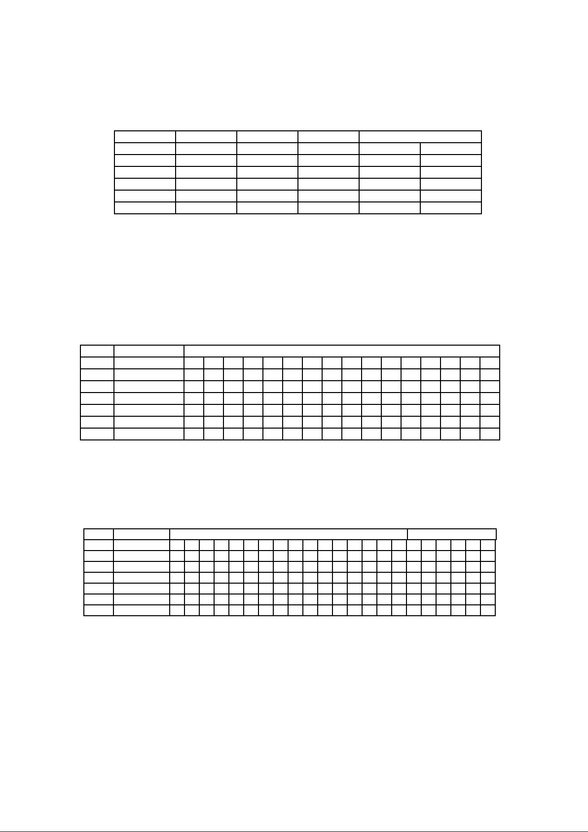
There are four signals which control the drive status of the EDAC external busses: RDWN, CS2N, CS1N and CS0. The
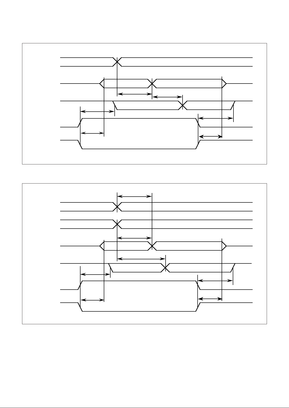
relationship to each other and to the EDAC busses is shown in Figure 2 below. The timing of these signals is shown in Figures 6
and 7.
Figure 2: Bus Control
2.3 INTERNAL OPERATION
2.3.1 Check Bit Generation
On write cycles the processor data word, PD[0:15], and the processor parity bit ,PD[16], are passed directly to the memory
data bus, MD[0:15], and the memory parity bit, MD[16].
The check bits, CB[0:5], are derived by 6 parity generators operating on sets of 8 bits of the processor data word, PD[0:15], as
shown in Figure 3 below:
Figure 3: Check Bit Generation
2.3.2 Syndrome Generation
The syndrome generation logic checks the sense of the check bits with respect to the memory data word. Six 9-input parity
checkers generate the syndrome bits, SY[0:5], according to figure 4 below:
Figure 4: Syndrome Generation
RDWN CS2N CS1N CS0 Bus state
Processor Memory
X High X X Tristate Tristate
X X High X Tristate Tristate
X X X Low Tristate Tristate
High Low Low High Output Input
Low Low Low High Input Output
CB Parity PD
15 14 13 12 11 10 9 8 7 6 5 4 3 2 1 0
0 Even X X X X X X X X
1 Even X X X X X X X X
2 Odd X X X X X X X X
3 Odd X X X X X X X X
4 Even X X X X X X X X
5 Even X X X X X X X X
If there are no errors in the memory data word, MD[0:15],
or the check bits, CB[0:5], then all of the syndrome bits,
SY[0:5], will be set low.
A single bit error in the memory data word, MD[0:15], will
cause 3 syndrome bits to be set high. However, a single bit
error in the check bits, CB[0:5], will cause only 1 syndrome bit
to be set high. A two bit error in the memory data word and/or
the check bits will cause either 2, 4, 5 or 6 syndrome bits to be
set.
Three or more errors in the memory data word and/or the
check bits will cause an undefined number of syndrome bits to
be set. This will cause the operation of the device in respect of
the states of CERRN, NCERRN and data on the PD bus to be
unpredictable.
S Y Parity MD CB
1514131211109876543210012345
0 Even X X XXXXX XX
1 Even X XXXX X X X X
2 Odd X X X X XXXX X
3 Odd X X X XXXXX X
4 Even X XXXXX X X X
5 Even XXXXX XX X X
Page 4
MA31755
4/13
2.3.3 Correction
With no syndrome bits set data will pass through from the
MD bus to the PD bus unchanged. When a single bit error
occurs in the memory data word, MD[0:15], the three
syndrome bits which are set identify which data bit is in error.
The correction logic decodes these syndrome bits and will
correct the error provided the correction enable input, ENCOR,
is high.
2.3.4 Flag Generation
The correctable error flag,CERRN, is driven low whenever
1 or 3 syndrome bits are set and flags are enabled (ENFLG=1).
The non-correctable error flag, NCERRN, is driven low
whenever 2, 4, 5 or 6 Syndrome bits are set and flags are
again enabled (ENFLG=1). NCERRN will also be driven low
should the external error input, XERRN, be driven low at any
time. Note: this external error feedthrough from XERRN to
NCERRN operates independently of ENFLG and the Chip
Select inputs (CS0, CS1N & CS2N).
Flags are enabled provided the ENFLG input is high and
the device is selected. Note: the flags are not disabled on write
cycles and therefore can indicate errors on write operations
caused by faults on the Memory Data Bus and the Check Bit
Bus.
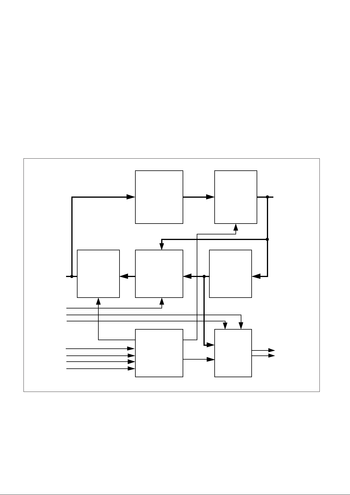
2.3.5 Internal Structure
Figure 5 below shows the internal block diagram
representing the internal architecture of the MA31755.
Figure 5: Block Diagram of the Internal Architecture of the MA31755
Check bit
generation
Tri-statable
Buffer
Tri-statable
Buffer
Correction
Syndrome
Generation
MD[0:16]
CB[0:5]
CERRN
NCERRN
PD[0:16]
ENCOR
ENFLG
XERRN
RDWN
CS0
CS1N
CS2N
Buffer
Control
Flags
Generation
Page 5
MA31755
5/13
3. TIMING DIAGRAMS
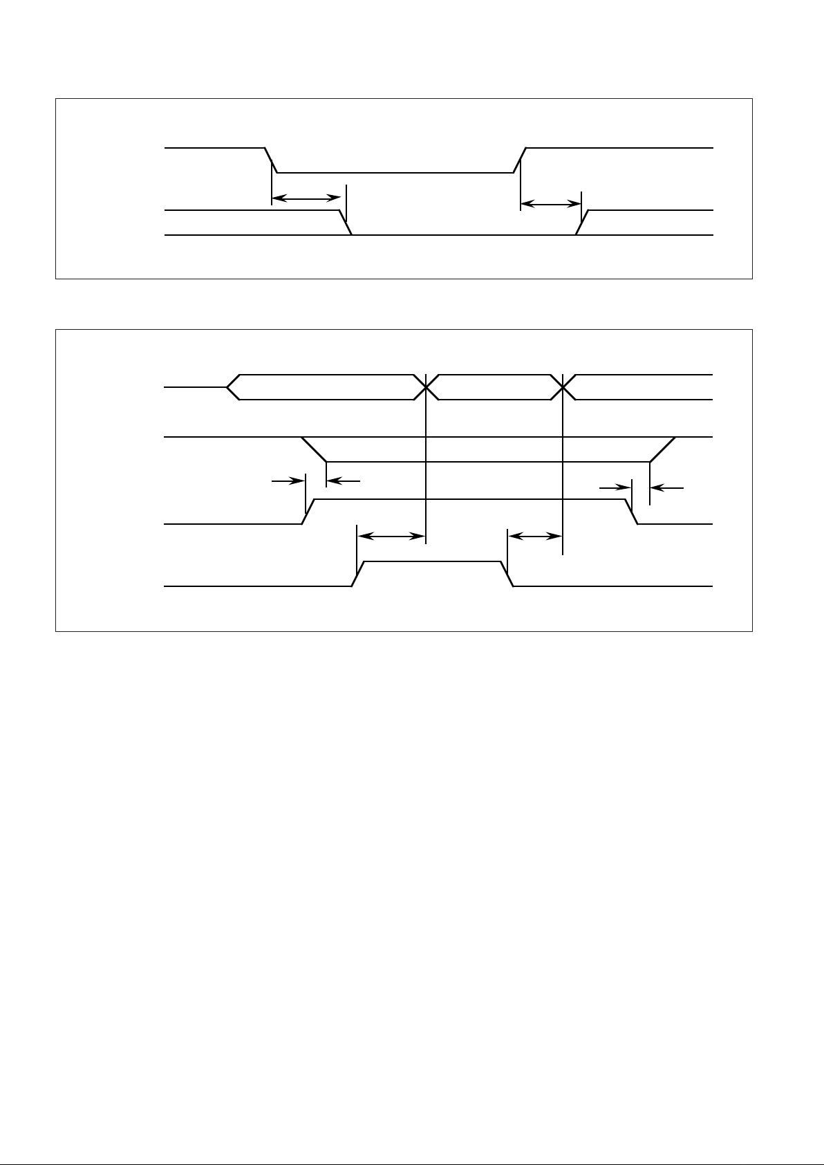
Figure 6 : Processor Write Timings (ENFLG = 1)
Figure 7: Processor Read Timings (ENCOR and ENFLG=1)
MD[0:16]
CB[0:5]
PD[0:16]
CERRN
NCERRN
Valid Flags
Data and check bits to memory
Data from processor
T1
T10
T9
CS0
CS1N
CS2N
RDWN
T4
T6
T8
MD[0:16]
PD[0:16]
Data from memory
RDWN
CS0
T2
CERRN
NCERRN
CS1N
CS2N
T5
T7
Valid Data
Valid Flags
T4
T6
T8
Check bits from memory
CB[0:5]
T3
Page 6
MA31755
6/13
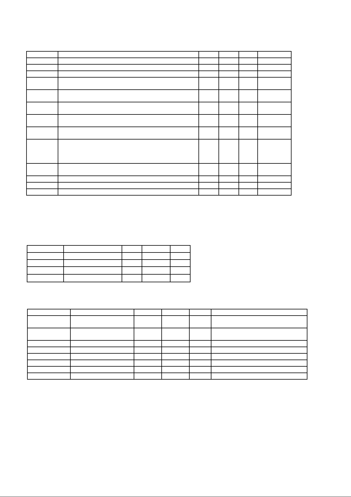
Figure 8: External Error Feedthrough Timing (ENFLG=X ,CS0=X, CS1N /CS2N=X)
Figure 9: Correction and Error flag enable/disable timings (CS0=1, CS1N/CS2N = 0)
T13
XERRN
NCERRN
T13
PD[0:16]
ENCOR
Corrected
Data
T12
CERRN
NCERRN
ENFLG
T11
T11
Uncorrected
Data
T12
Uncorrected
Data
Flags Valid
Page 7
MA31755
7/13
4. AC CHARACTERISTICS
5. DC CHARACTERISTICS AND RATINGS
Symbol Description Min. Max. Units
VDD Supply voltage -0.5 7 V
VI Input voltage -0.3 VDD+0.3 V
TA Operating temperature -55 +125
o
C
TS Storage temperature -65 +150
o
C
Note: Stresses above those listed may cause permanent
damage to the device. This is a stress rating only and
functional operation of the device at these conditions, or
at any other condition above those indicated in the
operations section of this specification, is not implied.
Exposure to absolute maximum rating conditions for
extended periods may affect device reliability.
Figure 11: Absolute Maximum Ratings
Conditions VDD = 4.5 to 5.5V, TA = -55 to +125°C
Mil-Std-883, method 5005, subgroups 1, 2, 3
Note 1: Worst case at TA = +125°C, guaranteed but not tested at TA = -55°C.
Parameter Description Min Max Units Notes
T1 PD[0:16] to MD[0:16] , CB[0:5] valid - 25 ns CL = 150pF
T2 MD[0:16] to PD[0:16] valid - 30 ns CL = 50pF
T3 CB[0:5] to PD[0:16] valid - 35 ns CL = 50pF
T4 MD[0:16] to CERRN and NCERRN valid
CB[0:5] to CERRN and NCERRN valid
- 40 ns CL = 50pF
T5 RDWN, CS0 rising to PD[0:16] driven (processor read)
CS1N, CS2N falling to PD[0:16] driven (processor read)
5 20 ns CL = 50pF
T6 CS0 rising to error flags changing
CS1N, CS2N falling to error flags changing
- 25 ns CL = 50pF
T7 RDWN, CS0 falling to PD[0:16] Hi-Z
CS1N,CS2N rising to PD[0:16] Hi-Z
- 30 ns CL = 50pF
T8 CS0 falling to error flags high
CS1N, CS2N rising to error flags high
- 25 ns CL = 50pF
T9 RDWN, CS1N and CS2N falling to MD[0:16] and CB[0:5]
driven (processor write)
CS0 rising to MD[0:16] and CB[0:5] driven (processor
write)
5 20 ns CL = 150pF
T10 CS0 falling to MD[0:16] and CB[0:5] Hi-Z
RDWN, CS1N, CS2N rising to MD[0:16] and CB[0:5] Hi-Z
5 25 ns CL = 150pF
T11 ENFLG to CERRN and NCERRN valid - 20 ns CL = 50pF
T12 ENCOR to PD[0:16] valid - 20 ns CL = 50pF
T13 XERRN to NCERRN valid - 10 ns CL = 50pF
Mil-Std-883, method 5005, subgroups 9, 10, 11
Figure 10: Timing Parameters
Parameter Description Min M ax Unit Notes
VOH Output high voltage Vdd- 0.5 - V IOH = 15mA on MD[0:16] / CB[0:5]
IOH = 5mA on other outputs.
VOL Output low voltage - Vss+0.5 V IOL = -15mA on MD[0:16] / CB[0:5]
IOL = -5mA on other outputs.
VIH Input high voltage Vdd-1.5 - V
VIL Input low voltage - Vss+1.5 V
IIL, IIH (Note 1) Input current high/low - 10 uA
IOZ (Note 1) Output tri-state leakage - 0.1 mA VO = 0 to V D D
ISS Standby current - 10 mA
IDD Operating current - 100 mA
Figure 12: Operating Electrical Characteristics
Page 8
MA31755
8/13
Subgroup Definition
1 Static characteristics specified in Figure 12 at +25°C
2 Static characteristics specified in Figure 12 at +125°C
3 Static characteristics specified in Figure 12 at -55°C
7 Functional characteristics specified at +25°C
8A Functional characteristics specified at +125°C
8B Functional characteristics specified at -55°C
9 Switching characteristics specified in Figure 10 at +25°C
10 Switching characteristics specified in Figure 10 at +125°C
11 Switching characteristics specified in Figure 10 at -55°C
Figure 13: Definition of Subgroups
6. APPLICATIONS INFORMATION
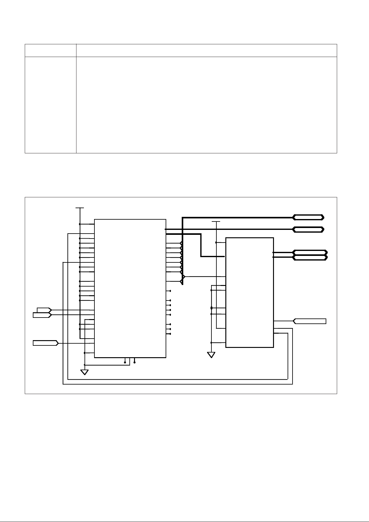
Figure 14: Basic System Diagram for the MA31755 with the MA31750
MA31750
ABN
ASTB
AS[0-3]
A[0-15]
CLK
CONREQN
DPARN
DSN
DTON
D[0-16]
EXADEN
FLT7N
GND
GRANTN
ILLADN
INT02N
INT08N
INT10N
INT11N
INT13N
INT15N
INTAKN
IOI1N
IOI2N
LOCKN
M/ION
MPROEN
NPU
O/IN
PB[0-3]
PEN
PS[0-3]
PWRDN
R/WN
RDN
RDYN
REQN
RESETN
SUREN
SYSFN
TCLK
TGON
VDD
WRN
MA31755
ENPDN
ENMDN
CERRNCS0
CB[0:5]
MD[0:16]
NCERRN
CS1N
RDWN
PD[0:16]
VDD0-3
VSS0-3
CONTROL
A[0-15]
PD[0:16]
ASTB
DSN
M/ION
MD[0:16]
RDWN
CB[0:5]
O/IN
RDN
WRN
RDWN
RDYN
CLK
TCLK
RESETN
To memory system
XERRN XERRN
CS2N
Page 9
MA31755
9/13
7. PACKAGING
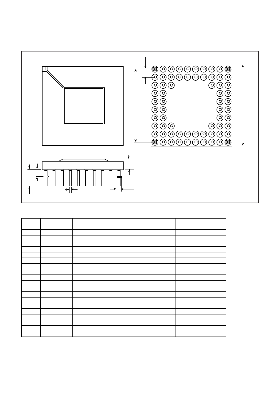
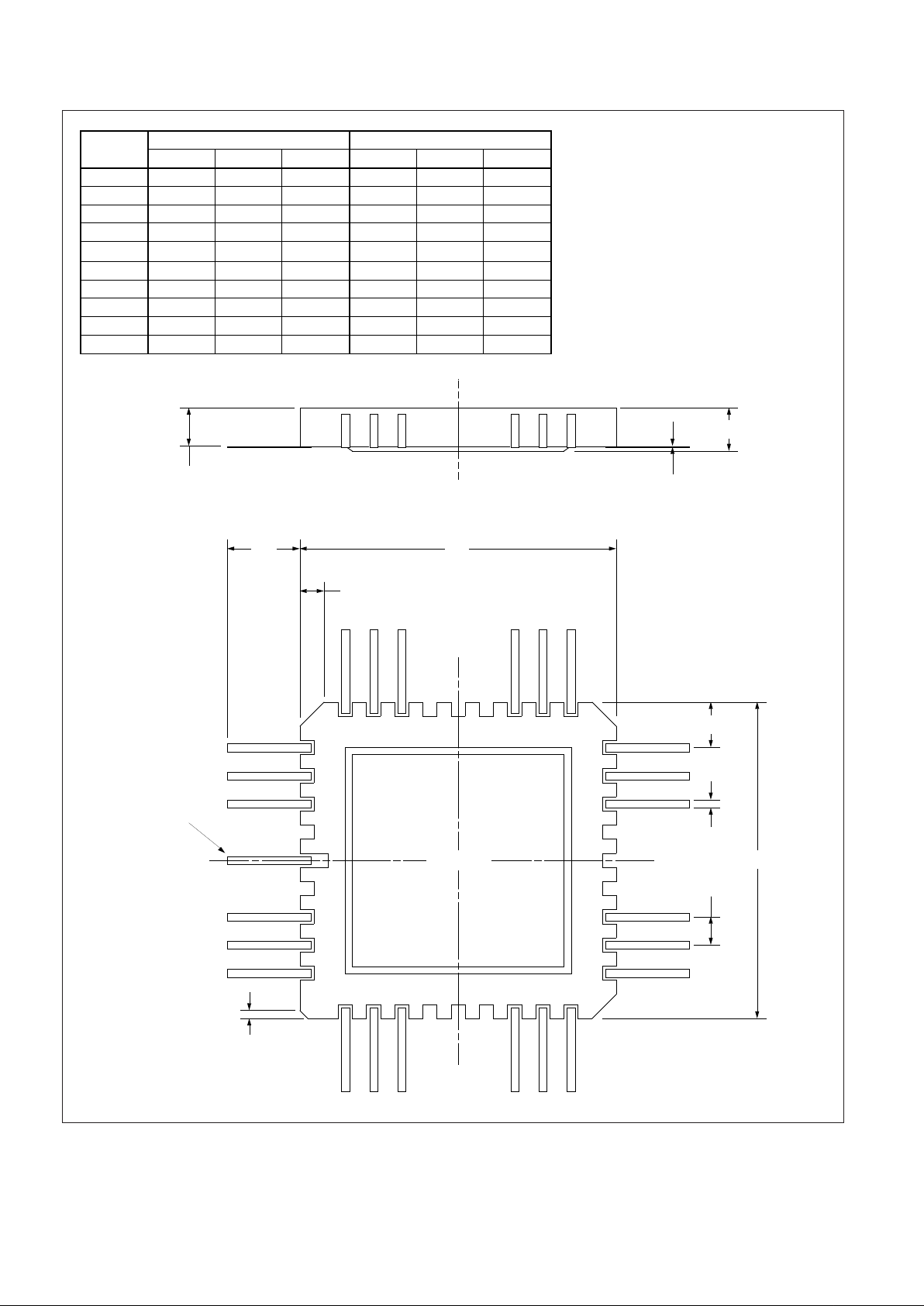
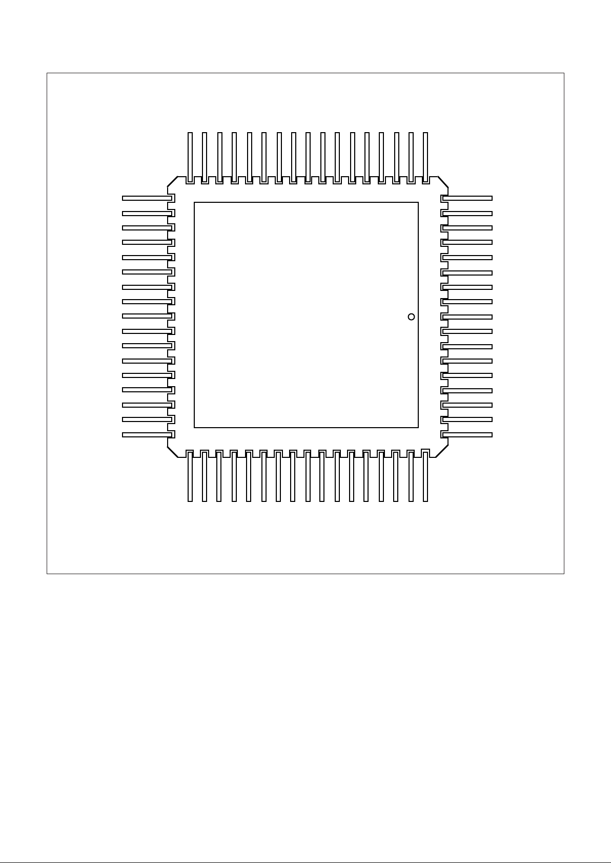
The device will be supplied in a 68-pin PGA for development with a 68-pin flatpack option for flight parts.
Figure 15: Dimensioned Drawing for the 68-pin PGA Package
Figure 16: Pinout for the 68-pin PGA Package
Pin Function Pin Function Pin Function Pin Function
A1 CB05 C1 CB02 G9 CS0 K3 MD08
A2 NCERRN C2 CB04 G10 PD00 K4 MD06
A3 RDWN C3 VDD H1 MD15 K5 VDD
A4 PD16 C8 VDD H2 MD12 K6 NC
A5 PD14 C9 PD07 H3 VDD K7 MD04
A6 VDD C10 PD04 H8 VDD K8 MD03
A7 PD13 D1 CB00 H9 ENFLG K9 MD01
A8 PD11 D2 CB01 H10 CS1N K10 ENCOR
A9 PD10 D9 PD05 J1 MD13
A10 PD08 D10 PD03 J2 GND
B1 CB03 E1 GND J3 MD10
B2 GND E2 NC J4 MD07
B3 CERRN E9 PD02 J5 GND
B4 XERRN E10 PD01 J6 MD05
B5 PD15 F1 VDD J7 MD02
B6 GND F2 NC J8 MD00
B7 PD12 F9 GND J9 GND
B8 PD09 F10 VDD J10 CS2N
B9 GND G1 MD16 K1 MD11
B10 PD06 G2 MD14 K2 MD09
BOTTOM
VIEW
1
2
3
4
5
6
7
8
9
10
A B C D E F G H J K
0.050
±0.010
0.900
±0.010
0.018
±0.002
0.105 max
1.060 sq
±0.020
0.100
0.180 ±0.010
0.045 ±0.005
TOP
VIEW
Pin A1 Index
XG451 Outline
Page 10
MA31755
10/13
Figure 17: Dimensioned Drawing for the 68-pin Flatpack Package Topbraze
Top View
j1
D1L
Pin 1
j2
b
e
D2
Z
A1
A
c
Ref
Millimetres Inches
Min. Nom. Max. Min. Nom. Max.
A - - 2.72 - - 0.107
A1 1.83 - 2.24 0.072 - 0.088
b 0.41 - 0.51 0.016 - 0.020
c 0.20 - 0.30 0.008 - 0.012
D1, D2 23.88 - 24.51 0.940 - 0.960
e - 2.54 - - 0.050 j1 - 1.02 - - 0.040 j2 - 0.51 - - 0.020 L 10.16 - 10.54 0.400 - 0.415
Z 1.65 - 2.16 0.065 - 0.085
XG540
Page 11
MA31755
11/13
Pin 1
TOP VIEW
GND
MD12
MD13
MD14
MD15
MD16
CB0
VDD
GND
CB1
CB2
CB3
CB4
CB5
VDD
VDD
ENCOR
ENFLG
CS2N
CS1N
CS0
PD0
PD1
PD2
PD3
PD4
PD5
PD6
GND
VDD
PD8
PD9
PD10
PD11
PD12
PD13
PD14
PD16
RDWN
XERRN
NCERRN
CERRN
GND
GND
MD0
MD1
MD2
MD3
MD4
MD5
VDD
GND
MD6
MD7
MD8
MD9
MD10
VDD
PD15
2
1
3
4
5
6
7
8
9
64
63
62
61
60595857
1011121314151617181920212223242526
56555453525150494847464544
27
33
34
35
36
37
38
39
40
28
29
30
31
32
43
42
41
Index
68
67
66
65
NC
VDD
GND
PD7
VDD
GND
MD11
NC
NC
Figure 18: Pinout for the 68-pin Flatpack Package
Page 12

MA31755
12/13
8. RADIATION TOLERANCE
8.1 TOTAL DOSE RADIATION TESTING
For product procured to guaranteed total dose radiation
levels, each wafer lot will be approved when all sample
devices from each lot pass the total dose radiation test.
The sample devices will be subjected to the total dose
radiation level (Cobalt-60 Source), defined by the ordering
code, and must continue to meet the electrical parameters
specified in the data sheet. Electrical tests, pre and post
irradiation, will be read and recorded.
Dynex Semiconductor can provide radiation testing
compliant with Mil-Std-883 test method 1019, Ionizing
Radiation (Total Dose).
9. ORDERING INFORMATION
For details of reliability, QA/QC, test and assembly
options, see ‘Manufacturing Capability and Quality
Assurance Standards’ Section 9.
Unique Circuit Designator
S
R
Q
Radiation Hard Processing
100 kRads (Si) Guaranteed
300 kRads (Si) Guaranteed
Radiation Tolerance
AFPin Grid Array
Flatpack (Solder Seal)
Package Type
QA/QCI Process
(See Section 9 Part 4)
Test Process
(See Section 9 Part 3)
Assembly Process
(See Section 9 Part 2)
L
C
D
E
B
S
Rel 0
Rel 1
Rel 2
Rel 3/4/5/STACK
Class B
Class S
Reliability Level
MAx31755xxxxx
Total Dose (Function to specification)* 5x10⁵ Rad(Si)
Transient Upset (Stored data loss) 1x10¹¹ Rad(Si)/sec
Transient Upset (Survivability) >1x10
12
Rad(Si)/sec
Neutron Hardness (Function to specification) >1x10¹⁵ n/cm
2
Single Event Upset** <1x10
-10
Errors/bit day
Latch Up Not possible
* Other total dose radiation levels available on request
** Worst case galactic cosmic ray upset - interplanetary/high altitude orbit
Figure 19: Radiation Hardness Parameters
Page 13

MA31755
13/13
CUSTOMER SERVICE CENTRES
France, Benelux, Italy and Spain Tel: +33 (0)1 69 18 90 00. Fax: +33 (0)1 64 46 54 50
North America Tel: 011-800-5554-5554. Fax: 011-800-5444-5444
UK, Germany, Scandinavia & Rest Of World Tel: +44 (0)1522 500500. Fax: +44 (0)1522 500020
SALES OFFICES
France, Benelux, Italy and Spain Tel: +33 (0)1 69 18 90 00. Fax: +33 (0)1 64 46 54 50
Germany Tel: 07351 827723
North America Tel: (613) 723-7035. Fax: (613) 723-1518. Toll Free: 1.888.33.DYNEX (39639) /
Tel: (831) 440-1988. Fax: (831) 440-1989 / Tel: (949) 733-3005. Fax: (949) 733-2986.
UK, Germany, Scandinavia & Rest Of World Tel: +44 (0)1522 500500. Fax: +44 (0)1522 500020
These offices are supported by Representatives and Distributors in many countries world-wide.
© Dynex Semiconductor 2000 Publication No. DS3572-4 Issue No. 4.0 January 2000
TECHNICAL DOCUMENTATION – NOT FOR RESALE. PRINTED IN UNITED KINGDOM
HEADQUARTERS OPERATIONS
DYNEX SEMICONDUCTOR LTD
Doddington Road, Lincoln.
Lincolnshire. LN6 3LF. United Kingdom.
Tel: 00-44-(0)1522-500500
Fax: 00-44-(0)1522-500550
DYNEX POWER INC.
Unit 7 - 58 Antares Drive,
Nepean, Ontario, Canada K2E 7W6.
Tel: 613.723.7035
Fax: 613.723.1518
Toll Free: 1.888.33.DYNEX (39639)
This publication is issued to provide information only which (unless agreed by the Company in writing) may not be used, applied or reproduced for any purpose nor form part of any order or contract nor to be regarded
as a representation relating to the products or services concerned. No warranty or guarantee express or implied is made regarding the capability, performance or suitability of any product or service. The Company
reserves the right to alter without prior notice the specification, design or price of any product or service. Information concerning possible methods of use is provided as a guide only and does not constitute any
guarantee that such methods of use will be satisfactory in a specific piece of equipment. It is the user's responsibility to fully determine the performance and suitability of any equipment using such information and
to ensure that any publication or data used is up to date and has not been superseded. These products are not suitable for use in any medical products whose failure to perform may result in significant injury
or death to the user. All products and materials are sold and services provided subject to the Company's conditions of sale, which are available on request.
All brand names and product names used in this publication are trademarks, registered trademarks or trade names of their respective owners.
http://www.dynexsemi.com
e-mail: [email protected]
Datasheet Annotations:
Dynex Semiconductor annotate datasheets in the top right hard corner of the front page, to indicate product status. The annotations are as follows:-
T arget Information: This is the most tentative form of information and represents a very preliminary specification. No actual design work on the product has been started.
Preliminary Information: The product is in design and development. The datasheet represents the product as it is understood but details may change.
Advance Information: The product design is complete and final characterisation for volume production is well in hand.
No Annotation: The product parameters are fixed and the product is available to datasheet specification.
 Loading...