

Page 1
MA31753
1/30
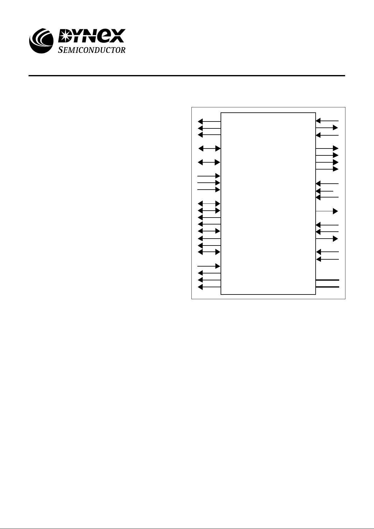
AS[0:3]
PS[0:3]
PB[0:3]
D[0:16]
A[0:15]
CSN
CLK
RESETN
DSN
AS
MION
OIN
RDWN
RDN
WRN
RDYN
GRANTN
REQN
LOCKN
DMAKN
DREQN[0:3]
DACKN[0:3]
DMAE
SEC/FIRSTN
DONEN
AKRDN
AKWRN
EXADEN
PEN
MPROEN
INTRN
REQINN
GEINN
GEOUTN
DPARN
DTON
VDD
VSS
MA31753
DMAC
The MA31753 Direct Memory Access Controller (DMAC) is
a peripheral interface circuit design primarily for use with the
MA31750 microprocessor. Each DMAC provides up to four
independant, prioritised channels each of which can perform
DMA transfers between memory and/or I/O devices using the
MA31750 bus. Each channel has its own programmable
internal priority and can be masked under program control.
Further, individual channels have their own associated status
and control words enabling an individual channel to be reprogrammed without disturbing transfers which may be taking
place on other channels. Three basic transfer modes are
available:
Direct Memory to I/O peripheral transfers,
Direct I/O to Memory transfers,
Memory to Memory transfers,
I/O to I/O transfers.
The MA31753 interfaces directly to the MA31750 bus,
directly supporting on chip parity generation and supporting
expanded memory via an MA31751 MMU with either 1 MWord
(1750A mode) or 16MWords (1750B mode) of logical memory.
The MA31753 uses System memory to hold address and
count information for each transfer. Once this information has
been prepared by the processor the DMAC can conduct a
number of transfers without further processor intervention.
FEATURES
■ Radiation Hard CMOS SOS Technology
■ Four Independant DMA Channels
■ MIL-STD-1750A or B Operation in an MA31750 System
■ Capable of Processor Independant Table Driven
Operation
■ Memory to Memory, I/O to Memory, Memory to I/O and
I/O to I/O Transfers Supported
■ Masking of Individual Channel DMA Requests
■ Simple MA31750 Bus Interface
■ Single Word, Double Word or Multi-Word Transfers for
each of the DMA Channels
■ Cascade Interface Allows for Channel Expansion
■ Programmable Channel Priority
■ Parity Checking Available
Figure 1: Pin Connections - Top View
MA31753
DMA Controller (DMAC) For An MA31750 System
Replaces June 1999 version, DS3825-4.0 DS3825-5.0 January 2000
Page 2
MA31753
2/30
1.0 GENERAL DESCRIPTION
The MA31753 DMA controller has 4 channels from which
independant transfers can be executed. These channels have
programmable priorities and can be masked. They can also be
enabled and disabled under software control.
The data can be transferred in several modes - single word
mode, double word mode and burst mode. It can be
transferred to and from both incrementing and decrementing
memory and IO addressing space. The single and double word
modes transfer data in 1 or 2 bus cycles when the simple
handshaking mechanism is enabled.
If more than 4 channels are required, several DMA
controllers can be cascaded together to give channel
expansion.
Once a channel has requested a transfer, and the bus
arbiter has granted bus control to the DMA, then the DMA
issues an acknowledge signal to the channel to be serviced. It
also pulses read or write strobes which can be gated with the
channel acknowledge signal to provide read and write strobes
for the requesting hardware.
DMA instructions can be programmed into memory on the
DMA. The transfers defined by these instructions can be
executed in sequence if they are “chained together”. In this
way, DMA transfers can take place continuously with data that
is held in seperate memory areas.
There is software access to all internal registers. These
registers have parity protection. By setting certain bits in
registers, requests can be initiated for area to area transfers on
channels 0 and 1. Interrupts for each channel can also be
issued.
2.0 INITIALISATION
After RESETN has been removed the DMA is
automatically initiated to be disabled with odd parity, the
channel priority order is 0, 1, 2, 3, C (C is the cascaded input)
and all channels are masked. At this point, before the DMA is
used further, the DMA instructions should be programmed into
the DMA internal RAM. Once all the instructions needed are in
place, the common features (ie. features that apply to all
channels) on the DMA can be programmed.These features
should be initialised to the users requirements.
The bus parity may be changed immediately after
RESETN goes inactive when the MA31750 reads the
configuration word ie. When the DMA detects the XIO address
0x8410, it snoops the data bus and latches the parity bit into an
internal copy. This internal copy can later be changed by
writing to the DMA Mode / Status register.
The DMA enable / disable follows the DMAE input - when
this input is high, the DMA device is enabled. When DMAE is
low, the DMA is disabled.
The channel priority and masking can be changed by
writing to the DMA Mode / Status register.
Once the common characteristics of the DMA have been
set up, the DMA individual channels can be programmed.
Each channel has a mode register that should be programmed
with an instruction number as that channel is activated (by
writing the mode word).
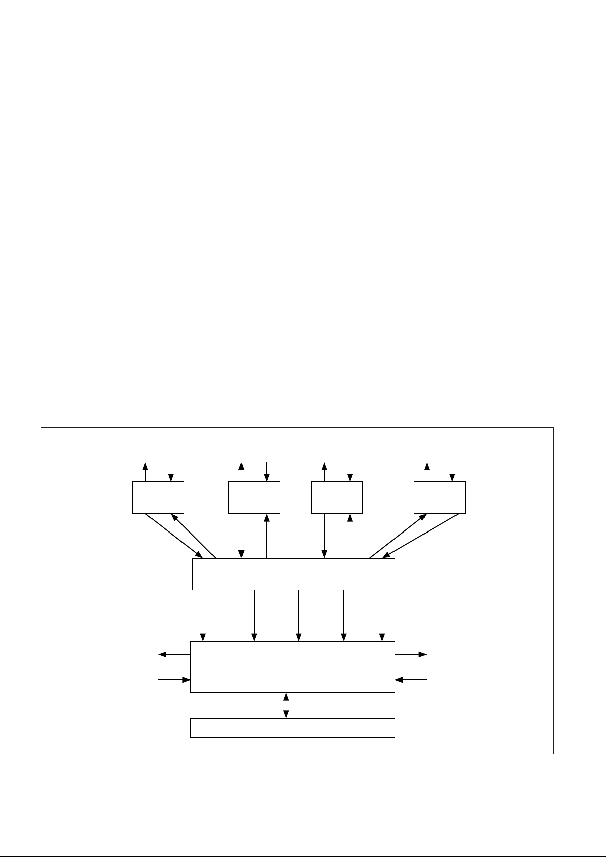
Figure 2: Block Diagram Representing the DMA Controller
Channel 1
Handler
Channel 2
Handler
Channel 3
Handler
Channel 4
Handler
PRIORITIZER
BUS MANAGER
BUS INTERFACE
DMA
req
DMA
ack
DMA
req
DMA
ack
DMA
req
DMA
ack
DMA
req
DMA
ack
DMARQN
A[0:15]
RDWN
Double
RDYN
Cascaded
request
out (REQN)
Bus grantn
(GRANTN)
Grant enable
out (GEOUTN
Cascaded grant
enable in
(GEINN)
Page 3

MA31753
3/30
3.0 DMA FUNCTIONALITY
Figure 2 shows a block diagram representing the structure
of the DMA controller. This figure also shows how the DMA
interfaces with the rest of the system.
Each DMA channel has 6 possible modes that it can
operate in. These are as follows:
3.1 IDLE MODE
The channel goes into IDLE mode after an active hardware
reset or after resetting the status flags. When in IDLE mode,
the channel goes into PEND_CHAIN mode when activated by
writing the Mode register. No parity check is done on this
register write.
3.2 PEND_CHAIN MODE
Once the channel has been activated, it goes from IDLE to
PEND_CHAIN mode. In this mode, the first instruction is read
(all 8 words). If a parity error is detected, the channel goes to
the ERROR mode. If the read is successful, the channel will
stay in the PEND_CHAIN mode until either an active request is
received or the Channel Request Pending bit is set in the
Channel Status Register. At this time, the channel progresses
to the PEND_REQ mode.
3.3 PEND_REQ MODE
In this mode, the Mode / Link word is checked to make sure
it doesn’t de-activate the channel (sending the device back to
IDLE mode). If the channel remains active, the device sits in
PEND_REQ mode until the system bus arbiter grants the DMA
bus control. Once this occurs, the transfer commences and the
DMA enters TRANSFER mode.
3.4 TRANSFER MODE
If at any time during the transfer an error occurs, the
channel is set into ERROR mode. If the transfers are clean of
errors, then the behaviour of the device is dependant on the
type of transfer mode that was programmed by the currently
executing instruction.
3.4.1 Single/Double Word and External Area to Area Mode
Within these modes, the DMA executes each data transfer
seperately, ie. between each single / double word transfer, the
request is removed. The DMA goes back into PEND_REQ
mode after each transfer and waits for the next request to be
granted.
3.4.2 Burst Area to Area Mode
With this type of transfer, the DMA transfers data whilst the
bus control is granted. The channel request signal remains
active. When control is removed by the arbiter, the device sits
in the PEND_TRANS mode until re-granted. If the burst mode
is area to area with interval timing, then between each transfer,
the channel has to count the interval.
Once a transfer has completed, the channel either sets the
EOT bit and sits waiting for this to be reset before it goes back
into INIT mode, or the instruction is chained and the channel
jumps back to the PEND_CHAIN mode where it can read the
next instruction details for the next transfer. If during any
transfer mode, the channel is de-activated, the channel goes
back to INIT mode. If at any time, an error is detected, the
device goes into ERROR mode.
3.5 ERROR MODE
This mode is entered from the PEND_CHAIN mode if a
parity error is detected during the instruction register reads.
The error mode can also be entered from theTRANSFER
mode. This can happen if PEN, MPROEN or EXADEN are
activated by trying to access one of the data transfer addreses.
An interrupt is generated in this mode. The only way to leave
this mode is to reset all the error flags.
3.6 WORD TRANSFER MODES
It is possible to run each channel in single, double, and
burst mode transfers.
3.6.1 Single Word Transfer
In single word transfer mode, the generation of each
request on a channel causes the DMA controller to issue an
external request that lasts for one bus cycle. The request is deactivated before the end of the bus cycle to allow other users to
aquire bus control. If the transfer is to or from a device needing
longer than one machine cycle (2 CLK cycles) then the cycle
can be extended using handshaking of the DMA request and
acknowledge lines.
3.6.2 Double Word Transfer
In double word mode, each request on a channel causes
the DMA controller to request bus control for 2 machine cycles
to allow the transfer of 2 16-bit data words. The data is
transferred to consecutive addresses and the bus is locked
between each word transfer to protect the transfer. The most
significant word to be transferred has the lowest address and
is transferred first (following the 1750 standard). The request is
de-activated before the end of the second bus cycle to allow
other bus users to take control. If an extended cycle is needed,
the handshaking mechanism doesn’t word in this mode and
the RDYN signal must be kept high for as long as required.
3.6.3 Burst Mode
In burst mode, one request to the channel causes the DMA
to request bus control for a complete block of data to be
transferred. The DMA de-asserts the request line on the last
transfer cycle to allow other users to take bus control.
Consequently, if the transfers are chained together, the CPU
may be able to get bus control between 2 blocks of data
transfer. If extended bus cycles are needed, the RDYN
mechanism can be used (handshaking does not work in this
mode).
Page 4

MA31753
4/30
3.6.4 Area to Area Mode
In area to area mode, the transfers can be initiated either
by external requests or internally generated by the DMA
depending on the value in the interval timer (the software
generated requests controlleed by the interval timer can only
be used on channels 0 and 1). Each request makes the DMA
request bus control for 2 machine cycles. The transfers can
take place to and from IO and / or memory depending on how
the instruction programs the channel. The DMA de-asserts the
request during the second cycle unless the instruction has
programmed the channel to do “Continuous Internal Request”.
In this case, the request is only de-asserted on the last cycle of
the block. If extended bus cycles are needed, the RDYN
mechanism must be used as the handshaking does not work in
this mode.
3.6.5 Instruction Chaining
When the first request is received on a channel, it
accesses the DMA instruction number that is programmed in
the mode word. This instruction is read from internal DMA
RAM. This takes 16 CLK cycles (as there are 8 16-bit word in
the instruction). Bus control is not needed during these internal
RAM accesses. At the end of the 16 CLK cycles, the channel
has all the transfer information it needs and can begin to
transfer whenever it is granted bus control. Once the transfer
has completed, the channel checks that it is in chaining mode
and that the instruction is a chained instruction. If so, then as
the first instruction completes, the DMA can access the next
instruction (again taking 16 CLK cycles) and the transfers can
continue as bus control is granted.
3.6.6 Handshaking Mechanism
There is a handshaking mechanism available when using
single-word transfer mode. It works as follows:
For a memory read cycle:
1: The IO port issues a request.
2: The DMA requests and is granted bus control. The DMA
starts a memory read cycle. As well as the usual control
and strobes, the DMA also asserts the DACKN low for the
channel that it is responding to. The DACKN signal acts as
an IO port select.
3: Once valid data is available on the data bus ie. RDYN has
gone low, the DMA asserts AKWRN low. The IO port uses
AKWRN as a write strobe.
4: The IO port acknowledges the completed data read by de-
asserting DREQN.
5: When the DMA sees DREQN has gone high, it de-asserts
DACKN. At this time, the data is still valid and the IO port
may latch the data on AKWRN rising or any time in
between.
6: The DMA completes the cycle by de-asserting strobes etc.
7: The wait state generator finally de-asserts RDYN.
For a memory write cycle:
1: The IO port issues a request.
2: The DMA aquires bus control and starts a memory write
cycle, also asserting DACKN for the relevant channel.
3: The data bus is driven by the IO port. Valid data is
available when the IO port de-asserts DREQN. (DACKN is
still asserted so valid data must still be driven on the bus).
4: When the DMA senses DREQN high, it writes the valid
data from the IO port into memory.
5: The memory write is completed when RDYN goes low.
6: The DMA de-asserts DACKN and hence the IO port stops
driving the data bus.
If DREQN is de-asserted 2 or more CLK cycles before
AKRDN or AKWRN are asserted, then the handshaking
protocol does not apply and the cycle will simply use the RDYN
signal going low to terminate the cycle (both AKRDN and
AKWRN will rise as AS falls at the end of the cycle).
3.7 INTERRUPT GENERATION
The DMA shall generate an interrupt on the occurrance of
any of the following:
- A channel has reached an “End of Transfer” condition and
the EOT bit has been set in the channel status register.
- A channel has been stopped because
a) a bus timeout has occurred. (ie. either DREQN
(handshake mode) or RDYN is asserted for more than
256 CLK cycles)
b) an internal parity error was detected when reading a
DMA register with parity.
c) An odd block length was programmed in double word
mode.
The DMA will stop but will not generate an interrupt if
EXADEN, MPROEN or PEN are active at the end of an
external cycle.
If a parity error is detected whilst writing to the DMA
registers, the erroneous write will not let transfers commence.
The DMA generates interrupts by pulsing INTRN low. If more
than one error occurs simultaneously, INTRN is only pulsed
once. The interrupt can only be generated when the DMA is in
the ERROR mode. The only way to get out of this mode is to
reset all error flags.
3.8 CHANNEL MASKING AND STOPPING
Each channel can be masked individually by setting the
relevant bit in the DMA Mode / Status register. If the channel is
masked, only external requests are gated out - software
requests are still serviced.
Each channel can be stopped by de-activating the channel
by writing the Channel Mode register. This register can only be
written whilst in PEND_CHAIN mode or awaiting bus control.
Once the channel is de-activated, it returns to the IDLE mode.
3.9 PARITY CHECKING
Parity checks are done when DMA registers are being
written and when they are being accessed ie. when the
instructions are being read.
Page 5

MA31753
5/30
3.10 SOFTWARE PROGRAMMING
DMA requests can be generated in software by writing the
CRQP bit in the Channel Status register. If the channel is
active, the DMA will then request bus control. If the DREQN
signal on that channel is not active, the DMA finishes the cycle
as soon as the memory is ready. There is no handshaking with
the IO port. DACKN is deasserted when the memory is ready.
If DREQN is asserted but is masked, the handshaking is active
and operates normally.
Interrupts can be generated in software by setting either a
channel EOT flag or any error flag. This can only be done
when the DMA is in PEND_CHAIN mode. If an error flag is set,
the device goes straight to ERROR mode. If the EOT flag is
set, the device looks as if it has completed the transfer. It will
then just sit and wait for the EOT flag to be cleared before
entering IDLE mode. If both flags are set simultaneously, the
device remains in PEND_CHAIN mode. Setting an error flag
when EOT is set resets EOT and the device goes to ERROR
mode. Setting EOT when an error flag is set clears the error
and the DMA sits in the finish transfer mode.
3.11 CASCADING DMA CONTROLLERS
DMA controllers are cascaded in series. For each DMA
added, an extra 4 channels become available. To cascade the
devices, the strobes, control signals and address and data
busses are connected in parallel. Of the bus arbitration
signals, LOCKN and GRANTN should be connected in parallel
and REQINN, GEINN and GEOUTN shoudl be daisy-chained.
INTRN and PEN can either be ORed together with external
glue logic or input to seperate CPU interrupts. Figure 3 shows
the cascade connections.
Figure 3: Cascading DMA Controllers
Bus
Arbiter
DMAC 1 DMAC 2
REQN
REQN
REQINN
GEOUTN
GEINN
DREQN[0:3]
DACKN[0:3]
Bus Interface Signals
DREQN[0:3]
DACKN[0:3]
Bus Interface Signals
GRANTN
44
4
4
Page 6

MA31753
6/30
4.0 DETAILED REGISTER DESCRIPTION
The internal registers on the DMA controller can be located
in either memory or IO addressing space. 32 words are control
registers and 480 words are the DMA instruction registers.
The address lines A[7:15] are used to decode the registers.
(A[0:6] are decoded to generate CSN low ie. the user can
place the DMA on the address map.)
4.1 MODE REGISTERS
CA read 0: channel not active
write 0: stop channel
read 1: channel active
write 1: start channel
This bit will be set low at an error or EOT condition
Mode 000: Single Word
001: Double Word
010: Burst Mode
011: Not used (channel not started)
100: Area to Area, Memory to Memory
101: Area to Area, Memory to IO
110: Area to Area, IO to Memory
111: Area to Area, IO to IO
A1M Area 1 Mode
For single, double and burst modes
00: Read from memory, incrementing address
01: Read from memory, decrementing address
10: Write to memory, incrementing address
11: Write to memory, decrementing address
Area to area mode
00: Area 1 address constant
01: Area 1 address incrementing
10: Area 1 address decrementing
11: Area 1 address constant
A2M Area 2 Mode (only used in area to area mode)
00: Area 2 address constant
01: Area 2 address incrementing
10: Area 2 address decrementing
11: Area 2 address constant
SEOT 0: Signal ‘End of Transfer’ at end of current block
only of C=0
1: Always signal ‘End of Transfer’ at end of
current block.
C read 0: Perform no chaining
read 1: Perform chaining using the value of “next
Instruction” field as pointer
write 0: Perform no chaining even if defined by current
DMA instruction
write 1: Perform chaining as defined by current
instruction
Next These 6 bits point to one of the 60 DMA instructions ie.
Inst the next instruction to be executed.
If the number is 3C, 3D, 3E or 3F, then the transfer will
stop with the current block (ie. no chaining)
A[7:15] Register Content Parity
0 DM A Instruction Yes
.. .
.. .
1DF DM A Instruction Yes
1E0 Channel 0 M ode No
1E1 Channel 0 R em aining w ords No
1E2 Channel 0 Area 1 current address No
1E3 Channel 0 Area 1 current PB/AS/PS No
1E4 Channel 0 Area 2 current address No
1E5 Channel 0 Area 2 current PB/AS/PS No
1E6 Channel 0 Status No
1E7 DM A M ode / Status 1 No
1E8 Channel 1 M ode No
1E9 Channel 1 R em aining w ords No
1EA Channel 1 Area 1 current address No
1EB Channel 1 Area 1 current PB/AS/PS No
1EC C hannel 1 Area 2 current address No
1ED C hannel 1 Area 2 current PB/AS/PS No
1EE Channel 1 Status No
1EF RESERVED No
1F0 Channel 2 Mode No
1F1 Channel 2 Rem aining w ords No
1F2 Channel 2 Area 1 current address No
1F3 Channel 2 Area 1 current PB/AS/PS No
1F4 Channel 2 Area 2 current address No
1F5 Channel 2 Area 2 current PB/AS/PS No
1F6 Channel 2 Status N o
1F7 RESERVED No
1F8 Channel 3 Mode No
1F9 Channel 3 Rem aining w ords No
1FA Channel 3 Area 1 current address No
1FB Channel 3 Area 1 current PB/AS/PS No
1FC Channel 3 Area 2 current address No
1FD Channel 3 Area 2 current PB/AS/PS No
1FE Channel 3 Status N o
1FF RESER VED No
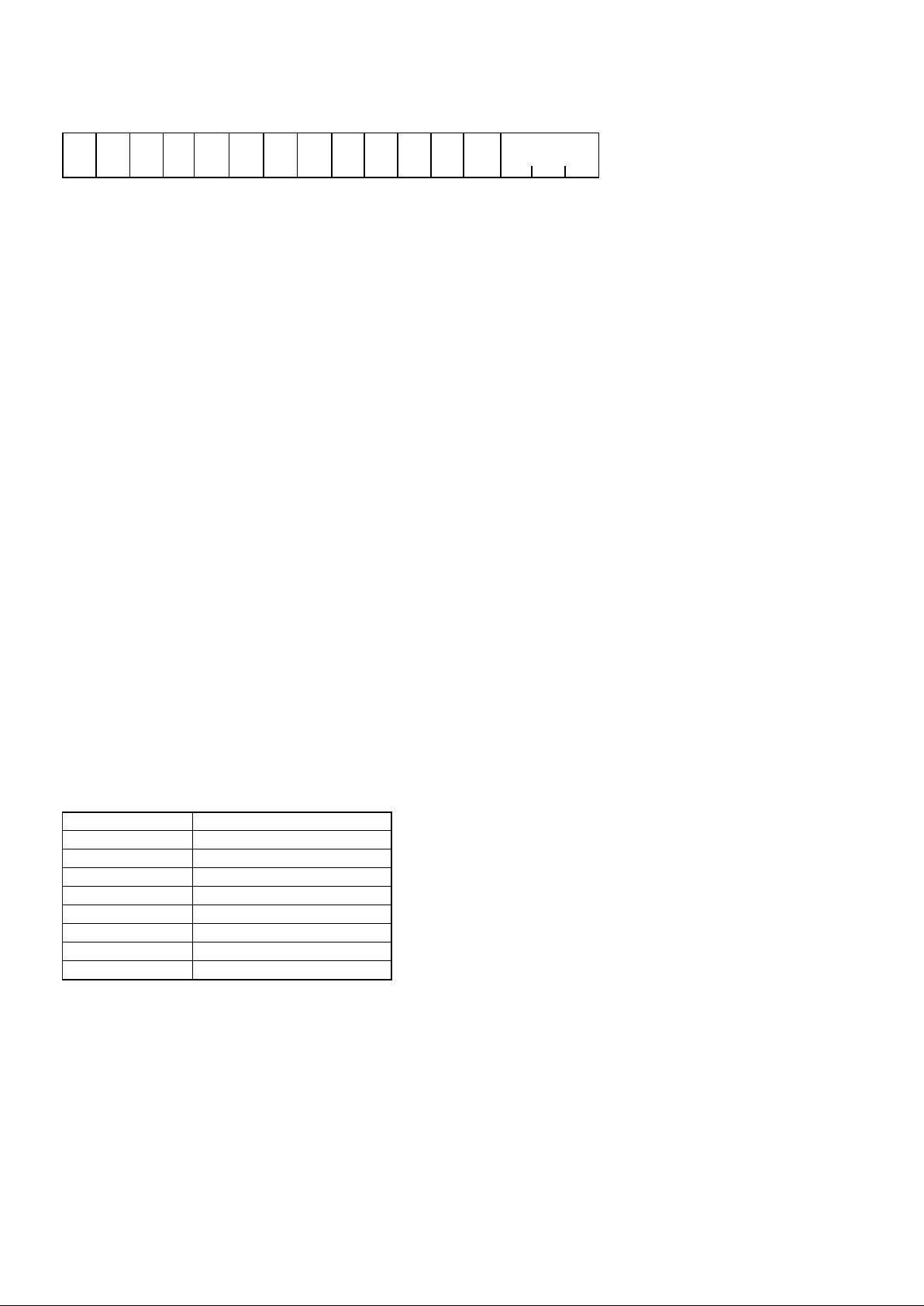
Mode Register
CA Mode A1M A2M SEOT C Next Instruction
D0 D15
Page 7

MA31753
7/30
4.2 REMAINING WORD REGISTERS
Read access only. These 16-bit registers store the number of words left to be transferred for each area.
4.3 CURRENT ADDRESS REGISTERS
Read access only. These 16-bit registers store the addresses of the current words to be transferred to / from the area
represented by the register.
4.4 CURRENT PB / PS / AS REGISTER
Read access only. These 16-bit registers store the current page bank, address and process state information for each area.
When the areas have been selected within the IO space, PB, PS and AS shall be zero.
4.5 STATUS REGISTERS
CA 0: Channel not active
1: Channel active
This bit is automatically set to zero at an error or EOT condition.
EOT 0: Channel EOT not reached
1: Channel EOT reached.
CRQP 0: No channel DMA request pending.
1: Channel DMA request pending.
It is not possible to reset this bit as long as a DREQN line is asserted.
IPE 0: No internal parity error
1: Internal parity error when reading DMA register with parity.
BLE 0: No error
1: Block length error (odd block length in double word mode)
BIE 0: No error
1: Bus interface timeout error (caused either by not deasserting DREQN in handshake mode or by a bus timeout)
CLE 0: No error
1: CPU latched error (either MPROEN, EXADEN or PEN)
Interval The interval, in CLK cycles, between each DMA request generated during area to area transfers.
Current Block Counter
D0 D15
Current Address
D0 D15
OIN PB0 PB3 PS0 PS3 AS0 AS3
D0 D15
CA EOT CRQP IPE BLE BIE CLE
Interval
D0 D15
Page 8
MA31753
8/30
4.6 DMA MODE / STATUS 1
Mn 0: Channel n not masked
1: Channel n masked
EOTn 0: Channel n “End of Transfer” not reached
1: Channel n “End of Transfer” reached
Read access only. Value can be changed by writing the channel status register.
ERR 0: No error detected
1: Error detected in one or more of the channels
Read access only. Value can be changed by writing the channel status register.
A / B 0: 1750A mode
1: 1750B mode
BP 0: Even bus parity used
1: Odd bus parity used
DMAE 0: DMA requests disabled
1: DMA requests enabled
Read access only
Pri 000: Channel priority 0, 1, 2, 3, C
001: Channel priority 1, 2, 3, 0, C
010: Channel priority 2, 3, 0, 1, C
011: Channel priority 3, 0, 1, 2, C
100: Channel priority C, 0, 1, 2, 3
101: Channel priority C, 1, 2, 3, 0
110: Channel priority C, 2, 3, 0, 1
111: Channel priority C, 3, 0, 1, 2
5.0 DMA INSTRUCTIONS
60 DMA instructions are present in the memory or IO space between A[7:15] = 0 and A[7:15] = 1DF. Each DMA instruction
comprises of 8 16-bit words. The base address for each instruction is 8*n where n is the instruction number. The instructions are
structured as below:
Words 4, 5 and 6 are used only during area to area mode transfers. Word 6 can only be used for channels 0 and 1.
M3
M2
M1
M0 EOT3 EOT2 EOT1 EOT0 ERR A/B BP DMAE Priority
D0 D15
Word number Content
0 Mode/Link word
1 Block length
2 Area 1 base address
3 Area 1 PB, PS and AS
4 Area 2 base address
5 Area 2 PB, PS and AS
6 Transfer interval
7 Not used
Page 9

MA31753
9/30
5.1 MODE / LINK WORD
Mode 000: Single word
001: Double word
010: Burst mode
011: not used (channel not started)
100: Area to Area, Memory to Memory
101: Area to Area, Memory to IO
110: Area to Area, IO to Memory
111: Area to Area, IO to IO
A1M Area 1 Mode
For single, double and burst modes
00: Read from memory, incrementing address
01: Read from memory, decrementing address
10: Write to memory, incrementing address
11: Write to memory, decrementing address
Area to area mode
00: Area 1 address constant
01: Area 1 address incrementing
10: Area 1 address decrementing
11: Area 1 address constant
A2M Area 2 Mode (only used in area to area mode)
00: Area 2 address constant
01: Area 2 address incrementing
10: Area 2 address decrementing
11: Area 2 address constant
SEOT 0: Signal ‘End of Transfer’ at end of current block only of C=0
1: Always signal ‘End of Transfer’ at end of current block.
C read 0: Perform no chaining
read 1: Perform chaining using the value of “next Instruction” field as pointer
write 0: Perform no chaining even if defined by current DMA instruction
write 1: Perform chaining as defined by current instruction
Next These 6 bits give the number of the next instruction to be executed. If the number is 3C, 3D, 3E or 3F, then the DMA
Inst transfers will stop with the current block.
5.2 BLOCK LENGTH
This readable and writable 16-bit word gives the number of words to be transferred for the current DMA block.
5.3 AREA 1 AND 2 BASE ADDRESSES
These registers hold the addresses of the first word of memory or IO to be transferred (ie. when the channel is decrementing
the address, this register holds the highest address to be transferred.)
Mode A1M A2M SEOT C Next Instruction
D0 D15
Block Length
D0 D15
Base Address
D0 D15
Page 10

MA31753
10/30
5.4 AREA 1 AND 2 PB, PS AND AS
These readable and writable registers store the Page Bank, Processor and Address State information to be used when
accessing areas 1 and 2. When areas are defined within IO space, PB, PS and AS are set to zero.
5.5 TRANSFER INTERVAL
This readable and writable register gives the number of CLK cycles between each DMA request generated during area to
area transfers. The number entered as the interval value corresponds to a clock cycle interval increasing by 32 as follows:
0 => - (externally triggered DMA requests)
1 => 0 (continuous DMA requests until the block is completed.
2=>32
3=>64
4=>96
.. .. ..
14 => 416
15 => 448
This function is valid only for transfers on channels 0 and 1. Channels 2 and 3 work ony only on externally triggered requests.
5.6 CONFIGURATION WORD
The DMA controller snoops the system address bus for the XIO address 0x8410. When this appears, the DMA stores the data
bus (qualified by DSN low) in an internal copy of the CPU configuration word.
OIN
PB0 PS0 AS0PB3 PS3 AS3
D0 D15
Interval
D0 D15
Page 11

MA31753
11/30
6.0 PIN DESCRIPTIONS
A[0:15] I/O A[0] is the most significant bit of this logical address bus. This bus is an input during cycles not assigned to the
DMA and is driven during DMA cycles.
PB[0:3] O Used in 1750B mode only, this bus provides DMA page bank information which addresses up to 8M of memory.
The bus is tri-stated during cycles not assigned to the DMA.
AS[0:3] O This bus indicates the current address state of the DMA controller. It is tri-stated during cycles not assigned to the
DMA.
PS[0:3] O This bus indicates the current process state of the DMA controller. It is tri-stated during cycles not assigned to the
DMA.
D[0:16] I/O D[0] is the most significant bit of the data bus. During DMA cycles, data is input on read cycles and output on write
cycles. D[16] is the parity bit. Odd or even parity is set in the configuration word. Parity is not used during DMA
writes to memory.
CLK I Input clock signal
RESETN I This active low signal resets the DMA.
CSN I When low, access to read and write the DMA internal registers is enabled.
AS I/O AS high indicates the presence of a valid address on the address bus. This signal is an input on cycles not
assigned to the DMA.
DSN I/O When low, data strobe indicates the presence of data on the data bus. This signal is an input on cycles not assigned
to the DMA.
MION I/O If high, this signal indicates that the current cycle is accessing memory space. If low, the current cycle is
accessing IO space. Is an input during cycles not assigned to the DMA.
RDWN I/O During DMA cycles, this signal goes high to indicate read cycles and low to indicate write cycles. It is an input
during non-DMA cycles.
OIN O During DMA cycles, this signal goes high to indicate operand cycles and low to indicate instruction cycles. It is tri-
stated during non-DMA cycles.
RDN O This active low read strobe is tri-stated on non-DMA cycles.
WRN O This active low write strobe is tri-stated on non-DMA cycles.
RDYN I/O This signal goes active low to indicate that the current bus cycles can be terminated. It is an output on cycles
addressing the DMA internal registers, input on cycles controlled by the DMA and is tri-stated during all other
cycles.
LOCKN O This signal is driven low during the first bus cycle of a double word transfer. It should be used by the bus arbiter to
'lock' bus control to the DMA. It is tri-stated during cycles not assigned to the DMA.
REQN O Always driven, this signal goes low to indicate that the DMA requests the bus.
GRANTN I Sampled by the DMA on negative CLK edges, this signal goes low to indicate that the DMA has bus control.
DMAKN O This output is driven active low by the DMA when it has bus control. It is tri-stated on cycles not assigned to the
DMA.
DONEN O This signal is pulsed low for one CLK cycle when any of the four DMA channels reaches an 'end of transfer'
condition.
REQINN I Sampled by the DMA on negative CLK edges, a low on this input indicates that a cascaded, lower priority DMA is
requesting the bus. This input should be tied high in a single DMA system.
GEINN I This active low signal is used to qualify the GRANTN signal for cascaded DMA devices. This signal should be tied
low on the first DMA of the chain.
GEOUTN O This active low output indicates that a lower priority DMA will be granted the bus when the GRANTN signal is
asserted low from the arbiter. It is used to cascade DMA devices by connecting to the GEINN pin of the next DMA.
INTRN O This active low interrupt request signal pulses low when an 'end of transfer' or an internal error condition are
detected.
PEN I The DMA samples PEN on AS falling. If an error condition is sampled, the transfer on the DMA channel is stopped
and the CLE bit is set in the Channel Status Register.
DMAE I An active high input to indicate that the DMA is enabled. If this input is low, internal requests are supressed, there is
no response to external requests and REQINN is gated out internally.
DPARN I A low on this signal resets and disables checking of the parity bit (D[16])
DTON I A low on this signal resets and disables the bus fault timeout circuitry.
MPROEN I This input is sampled on AS falling when the DMA has bus control. If an active low is sampled, the transfer stops
on the channel concerned and the CAE (addressing error) bit is set in the channel status register. An interrupt may
be generated.
EXADEN I This input is sampled on AS falling when the DMA has bus control. If an active low is sampled, the transfer stops
on the channel concerned and the CAE (addressing error) bit is set in the channel status register. An interrupt may
be generated.
DREQN[0:3] I Sampled by the DMA on negative CLK edges, a low on this bus initiates a DMA transfer providing the
corresponding channel is correctly set up and is not masked. When the pin is pulled high, the ongoing bus cycle
will terminate.
DACKN[0:3] O During a transfer, the DMA drives the relevant channel acknowledge low to indicate that the DMA is ready for the
data. The low to high transition at the end of the cycle is initiated by the condition DREQN high and RDYN low.
SEC/FIRSTN O A high indicates that the first word in a transfer is occuring. A low indicates that the second word in a double word
transfer is occuring.
AKRDN O This active low strobe indicates that the DMA is driving the data bus.
AKWRN O This active low strobe indicates that the DMA is inputting data from the data bus.
Page 12

MA31753
12/30
TIMING DIAGRAMS
Figure 4: Single Cycle With Handshake, Memory Read
CLK
DREQN
DACKN
AKWRN
AKRDN
DONEN
SEC/FIRSTN
REQN
GRANTN
A[0:15]
AS[0:3]
PS[0:3]
PB[0:3]
MION
OIN
RDWN
AS
DSN
WRN
RDN
LOCKN
RDYN
21
22
23
24
25
26 27
30
29
38 39
25
29
30 30
30
37
37
46
D[0:16]
54 55
Page 13

MA31753
13/30
CLK
DREQN
DACKN
AKRDN
AKWRN
DONEN
SEC/FIRSTN
REQN
GRANTN
A[0:15]
AS[0:3]
PS[0:3]
PB[0:3]
MION
OIN
RDWN
AS
DSN
RDN
WRN
LOCKN
RDYN
25
27
30
25
30
42
43
28
51
50
46
47
D[0:16]
52
53
Figure 5: Single Cycle With Handshake, Memory Write
Page 14

MA31753
14/30
Figure 6: Single Cycle Without Handshake, Memory Read
C
LK
DREQN
DACKN
AKWRN
AKRDN
DONEN
SEC/FIRSTN
REQN
GRANTN
AS
DSN
WRN
RDN
LOCKN
RDYN
A [0:15
]
MION
RDWN
OIN
DMAKN
Page 15

MA31753
15/30
C
LK
DREQN
DACKN
AKRDN
AKWRN
DONEN
SEC/FIRSTN
REQN
GRANTN
AS
DSN
RDN
WRN
LOCKN
RDYN
A [0:15
]
MION
RDWN
OIN
DMAKN
Figure 7: Single Cycle Without Handshake, Memory Write
Page 16

MA31753
16/30
Figure 8: Double Mode, Memory Read
C
LK
DREQN
DACKN
AKWRN
AKRDN
DONEN
SEC/FIRSTN
REQN
GRANTN
AS
DSN
WRN
RDN
LOCKN
RDYN
A [0:15
]
MION
RDWN
OIN
DMAKN
36
36
3534
Page 17

MA31753
17/30
Figure 9: Double Mode, Memory Write
C
LK
DREQN
DACKN
AKRDN
AKWRN
DONEN
SEC/FIRSTN
REQN
GRANTN
AS
DSN
RDN
WRN
LOCKN
RDYN
A [0:15
]
MION
RDWN
OIN
DMAKN
Page 18

MA31753
18/30
Figure 10: Burst Mode 6 Words, Memory Read
C
LK
DREQN
DACKN
AKWRN
AKRDN
DONEN
SEC/FIRSTN
REQN
GRANTN
AS
DSN
WRN
RDN
LOCKN
RDYN
A [0:15]
MION
RDWN
OIN
DMAKN
Page 19

MA31753
19/30
C
LK
DREQN
DACKN
AKRDN
AKWRN
DONEN
SEC/FIRSTN
REQN
GRANTN
AS
DSN
RDN
WRN
LOCKN
RDYN
A [0:15]
MION
RDWN
OIN
DMAKN
Figure 11: Burst Mode 4 Words, Memory Write (with interruption of the block)
Page 20

MA31753
20/30
Figure 12: DMA XIO read and write cycles
CLK
A[0:15]
CSN
DSN
MION
OIN
RDWN
RDN
WRN
RDYN
from
DMA
D[0:16]
AS
4
8
5
5
6
7
6
7
4
98 9
10
11
12
13
14
15
18
17
16
16
17
18
Page 21

MA31753
21/30
REQINN1
CLK
GEINN2
48
49
45
44
GEOUTN1
31
DREQN2
REQN2
GRANTN1
REQN1
Cascade Mode - DMA 2 = slave.
DMA 1 = master
42
43
31
48
DACKN2
Figure 13: Cascade Mode
RESETN
CLK
12
3
AS
MPROEN
EXADEN
PEN
40
41
CLK
INTRN
32
32
33
DONEN
CLK
DPARN
DTON
DMAE
56
57
58 59
60 61
Figure 14: Miscellaneous Timings
Page 22

MA31753
22/30
Mil-Std-883, Method 5005, Subgroups 9, 10, 11.
TL = Low CLK period (ns), TH = High CLK period (ns).
Test Conditions: Vdd = 5.0V ±10%, Temperature = -55oC to 125oC, Vil = 0.0V, Vih = Vdd.
Output loads: All test load 1 unless otherwise specified.
Output Threshold: 50% Vdd (Load 1), Vss+1V, Vdd-1V (Load 2).
Note 1: A[0:15], AS[0:3], PS[0:3], PB[0:3], MION, OIN, RDWN, DMAKN, AS, DSN, RDN, WRN, LOCKN
Figure 15: Timing Parameters
No. Description Min Max Units
1 RESETN setup to CLK falling - ns
2 RESETN hold after CLK falling - ns
3 RESETN pulse wdth - ns
4 A[0:15] setup to CSN falling (DMA XIO) - ns
5 A[0:15] hold after DSN rising (DMA XIO) - ns
6 CSN setup to DSN falling (DMA XIO) - ns
7 CSN hold after DSN rising (DMA XIO) - ns
8 MION, OIN, RDWN setup to AS rising (DMA XIO) - ns
9 MION, OIN, RDWN hold after AS falling (DMA XIO) - ns
10 RDN falling to D[0:16] driven (XIO read) ns
11 RDN falling to D[0:16] valid (XIO read) ns
12 RDN rising to D[0:16] invalid (XIO read) ns
13 RDN rising to D[0:16] tri-state (XIO read) ns
14 D[0:16] setup to WRN rising (XIO write) - ns
15 D[0:16] hold after WRN rising (XIO write) - ns
16 CLK falling to RDYN valid (DMA XIO) ns
17 CSN rising to RDYN tri-state (DMA XIO) ns
18 CSN falling to RDYN driven (DMA XIO) ns
19 CLK rising to AS rising ns
20 CLK falling to AS falling ns
21 A[0:15], AS[0:3], PS[0:3], PB[0:3] valid to AS rising ns
2 2 A[0:15], AS[0:3], PS[0:3], PB[0:3] valid after AS falling ns
23 MION, OIN, RDWN valid to DSN falling ns
24 MION, OIN, RDWN valid after DSN rising ns
25 CLK falling to AKRDN, AKWRN valid ns
26 CLK falling to DACKN[0:3] falling ns
27 CLK falling to DACKN[0:3] rising ns
28 CLK falling to DMAKN valid ns
29 CLK falling to DONEN valid ns
30 CLK falling to DSN, RDN, WRN valid ns
31 CLK falling to GEOUTN valid ns
32 CLK falling to INTRN valid ns
33 INTRN pulse width ns
34 CLK falling to LOCKN falling ns
35 CLK falling to LOCKN rising ns
36 CLK falling to SEC/FIRSTN valid ns
37 CLK falling to REQN valid ns
3 8 DREQN[0:3] setup to CLK falling - ns
39 DREQN[0:3] hold after CLK falling - ns
40 EXADEN, MPROEN, PEN setup to AS falling - ns
41 EXADEN, MPROEN, PEN hold after AS faling - ns
42 GRANTN setup to CLK falling - ns
43 GRANTN hold after CLK falling - ns
44 GEINN setup to CLK falling - ns
45 GEINN hold after CLK falling - ns
46 RDYN setup to CLK falling - ns
47 RDYN hold after CLK falling - ns
48 REQINN setup to CLK falling - ns
49 REQINN hold after CLK falling - ns
50 CLK rising to busses, strobes and control signals (note 1) tri-state ns
51 CLK falling to busses, strobes and control signals (note 1) driven ns
5 2 D[0:16] setup to AKRDN rising - ns
53 D[0:16] hold after AKRDN rising - ns
54 D[0:16] valid after AKWRN falling ns
55 D[0:16] valid after AKWRN rising ns
56 DPARN setup to CLK falling - ns
57 DPARN hold after CLK falling - ns
58 DTON setup to CLK falling - ns
59 DTON hold after CLK falling - ns
60 DMAE setup to CLK falling - ns
61 DMAE hold after CLK falling - ns
Page 23

MA31753
23/30
Figure 16: Absolute Maximum Ratings
RATING AND CHARACTERISTICS
Parameter Min. Max. Units
Supply voltage -0.5 7 V
Input voltage -0.3 VDD+0.3 V
Current through any I/O pin -20 20 mA
Operating temperature -55 125
o
C
Storage temperature -65 150
o
C
Note: Stresses above those listed may cause permanent
damage to the device. This is a stress rating only and
functional operation of the device at these conditions, or at any
other condition above those indicated in the operations section
of this specification, is not implied. Exposure to absolute
maximum ratings for extended periods may affect device
reliability.
Parameter Min. Max Units
Clock Frequency (CLK) 0 16 MH z
Recomm ended C lock duty cycle 45 55 %
Vdd=5V±10% over full operating temperature range
Mil-Std-883, method 5005, subgroups 1, 2, 3
Note 1: Guaranteed but not tested at low temperature (-55°C)
Figure 18: Operating DC Electrical Characteristics
Vdd=5V±10% over full operating temperature range
Mil-Std-883, method 5005, subgroups 7, 8A, 8B
Figure 17: Operating AC Electrical Characteristics
Tota l dos e ra dia t ion not
exceeding 3x10
5
Rad( S i)
Symbol Parameters Conditions Min Typ Max Units
V
DD
Supply voltage - 4.5 5.0 5.5 V
V
IH
Input high voltage - 80% V
DD
--V
VILInput low voltage - - - 20% V
DD
V
V
CKH
CLK input high voltage - VDD-0.5 - - V
V
CKL
CLK input low voltage - - - VSS+0.5 V
V
OH
Output high voltage IOH=-3m A VDD-0.5 - - V
V
OL
Output low voltage IOL=5mA - - VSS+0.4 V
I
IH
Input high current (Note 1) - - - 10 µA
I
IL
Input low current (Note 1) - - - -10 µA
I
OZH
I/O tristate high current (Note 1) - - - 50 µA
I
OZL
I/O tristate low current (Note 1) - - - -50 µA
I
DDYN
Dynamic supply current @ 16MH z - - - 80 mA
I
DDS
Static supply current - - - 10 mA
Page 24

MA31753
24/30
Subgroup Definition
1 Static characteristics specified in Figure 18 at +25°C
2 Static characteristics specified in Figure 18 at +125°C
3 Static characteristics specified in Figure 18 at -55°C
7 Functional characteristics specified in Figure 17 at +25°C
8A Functional characteristics specified in Figure 17 at +125°C
8B Functional characteristics specified in Figure 17 at -55°C
9 Switching characteristics specified in Figure 15 at +25°C
10 Switching characteristics specified in Figure 15 at +125°C
11 Switching characteristics specified in Figure 15 at -55°C
Figure 19: Definition of MIL-STD-883, Method 5005 Subgroups
Page 25

MA31753
25/30
PIN ASSIGNMENTS AND OUTLINES
Figure 20: 84-Lead Flatpack - Package Style F
RESETN
D00
D01
D02
D03
D04
D05
D06
D07
D08
D09
D10
DSN
RDWN
OIN
RDN
WRN
GRANTN
REQN
LOCKN
RDYN
CLKOUT
DPARN
DTON
TGON
NPU
SUREN
CONREQN
DMAE
DISCON
SNEW
CONFWN
PB3
PB2
PB1
PB0
AS3
AS2
AS1
AS0
INTAKN
VDD
AS
CLK
GND
A15
A14
A13
A12
A11
A10A9A8
A7A6A5A4A3
A2A1A0
MION
TCLK
D11
D12
D13
D14
D15
D16
MPROEN
PEN
EXADEN
FLT7N
SYSFN
BUSFAULTN
PWRDN
INT02N
INT08N
INT10N
INT11N
INT13N
INT15N
IOI1N
IOI2N
11
10
9
8
7
6
5
4
3
2
1
84
83
82
81
80
79
78
77
76
75
33
34
35
36
37
38
39
40
41
42
43
44
45
46
47
48
49
50
51
52
53
54 55 56 57 58 59 60 61 62 63 64 65 66 67 68 69
70 71 72 73 74
32 31 30 29 28 27 26 25 24 23
22 21 20 19 18 17 16 15 14 13 12
Pin 1 Index
TOP VIEW
Page 26

MA31753
26/30
11
10
9
8
7
6
5
4
3
2
1
84
83
82
81
80
79
78
77
76
75
33
34
35
36
37
38
39
40
41
42
43
44
45
46
47
48
49
50
51
52
53
54 55 56 57 58 59 60 61 62 63 64 65 66 67 68 69 70 71 72 73 74
32 31 30 29 28
27 26 25 24 23 22 21 20 19 18 17 16 15 14 13 12
Pin 1
Index
TOP
VIEW
Max
0.105
0.012
0.006
Nom
0.050
0.020
0.014
1.167
1.138
1.167
1.138
0.325
0.250
NOTE: All dimensions shown in inches
Figure 21: 84-Lead Flatpack - Package Style F
Page 27

MA31753
27/30
Figure 22: 84-Pin Grid Array - Package Style A
BOTTOM
VIEW
A
B
C
D
E
F
G
H
J
K
L
11 10 9 8 7 6 5 4 3 2 1
A1 B11 F9 K2
A2 C1 F10 K3
A3 C2 F11 K4
A4 C5 G1 K5
A5 C6 G2 K6
A6 C7 G3 K7
A7 C10 G9 K8
A8 C11 G10 K9
A9 D1 G11 K1 0
A10D2 H1K11
A11 D10 H2 L1
B1 D11 H10 L2
B2 E1 H11 L3
B3 E2 J1 L4
B4 E3 J2 L5
B5 E9 J5 L6
B6 E10 J6 L7
B7 E11 J7 L8
B8 F1 J10 L9
B9 F2 J11 L10
B10F3 K1L11
Page 28

MA31753
28/30
Notes:
1. represents gold plating 50 microns min.
over 100 microns nominal nickel.
2. All dimensions are in inches.
3. Default tolerances ±1% not less than 0.005
4. Ceramic is 92% Alumina.
Figure 23: 84-Pin Grid Array - Package Style A
BOTTOM
VIEW
A
B
C
D
E
F
G
H
J
K
L
11 10 9 8 7 6 5 4 3 2 1
Pin 1 Index
1.100
SQ
+/- .012
0.900
0.070 dia
0.105 MAX
0.100
0.050
+/- 0.004
0.180
=/-
0.004
0.008
0.050
+/-0.005
0.018
=/-0.00
2
Pin Detail
Page 29

MA31753
29/30
RADIATION TOLERANCE
Total Dose Radiation Testing
For product procured to total dose radiation levels, each
wafer lot will be approved when all sample devices pass the
total dose radiation test.
The sample devices will be subjected to the total dose
radiation level (Cobalt-60 Source), defined by the ordering
code, and must continue to meet the electrical parameters
specified in the data sheet. Electrical tests, pre and post
irradiation, will be read and recorded.
Dynex Semiconductor can provide radiation testing
compliant with MIL STD 883 test method 1019, Ionizing
Radiation (Total Dose).
Total Dose (Function to specification)* 3x10⁵ Rad(Si)
Transient Upset (Stored data loss) 1x10¹¹ Rad(Si)/sec
Transient Upset (Survivability) >1x10
12
Rad(Si)/sec
Neutron Hardness (Function to specification) >1x10¹⁵ n/cm
2
Single Event Upset**
<1x10
-10
Errors/bit day
Latch Up Not possible
* Other total dose radiation levels available on request
** Worst case galactic cosmic ray upset - interplanetary/high altitude orbit
Figure 24: Radiation Hardness Parameters
Page 30

MA31753
30/30
ORDERING INFORMATION
For details of reliability, QA/QC, test and assembly
options, see ‘Manufacturing Capability and Quality
Assurance Standards’ - SOS Handbook Section 9.
S
R
Q
Radiation Hard Processing
100 kRads (Si) Guaranteed
300 kRads (Si) Guaranteed
Radiation Tolerance
AFPin Grid Array
Flatpack (Solder Seal)
Package Type
QA/QCI Process
(See Section 9 Part 4)
Test Process
(See Section 9 Part 3)
Assembly Process
(See Section 9 Part 2)
L
C
D
E
B
S
Rel 0
Rel 1
Rel 2
Rel 3/4/5/STACK
Class B
Class S
Reliability Level
MAx31753xxxxx
Unique Circuit Designator
CUSTOMER SERVICE CENTRES
France, Benelux, Italy and Spain Tel: +33 (0)1 69 18 90 00. Fax: +33 (0)1 64 46 54 50
North America Tel: 011-800-5554-5554. Fax: 011-800-5444-5444
UK, Germany, Scandinavia & Rest Of World Tel: +44 (0)1522 500500. Fax: +44 (0)1522 500020
SALES OFFICES
France, Benelux, Italy and Spain Tel: +33 (0)1 69 18 90 00. Fax: +33 (0)1 64 46 54 50
Germany Tel: 07351 827723
North America Tel: (613) 723-7035. Fax: (613) 723-1518. Toll Free: 1.888.33.DYNEX (39639) /
Tel: (831) 440-1988. Fax: (831) 440-1989 / Tel: (949) 733-3005. Fax: (949) 733-2986.
UK, Germany, Scandinavia & Rest Of World Tel: +44 (0)1522 500500. Fax: +44 (0)1522 500020
These offices are supported by Representatives and Distributors in many countries world-wide.
© Dynex Semiconductor 2000 Publication No. DS3825-5 Issue No.5.0 January 2000
TECHNICAL DOCUMENTATION – NOT FOR RESALE. PRINTED IN UNITED KINGDOM
HEADQUARTERS OPERATIONS
DYNEX SEMICONDUCTOR LTD
Doddington Road, Lincoln.
Lincolnshire. LN6 3LF. United Kingdom.
Tel: 00-44-(0)1522-500500
Fax: 00-44-(0)1522-500550
DYNEX POWER INC.
Unit 7 - 58 Antares Drive,
Nepean, Ontario, Canada K2E 7W6.
Tel: 613.723.7035
Fax: 613.723.1518
Toll Free: 1.888.33.DYNEX (39639)
This publication is issued to provide information only which (unless agreed by the Company in writing) may not be used, applied or reproduced for any purpose nor form part of any order or contract nor to be regarded
as a representation relating to the products or services concerned. No warranty or guarantee express or implied is made regarding the capability, performance or suitability of any product or service. The Company
reserves the right to alter without prior notice the specification, design or price of any product or service. Information concerning possible methods of use is provided as a guide only and does not constitute any
guarantee that such methods of use will be satisfactory in a specific piece of equipment. It is the user's responsibility to fully determine the performance and suitability of any equipment using such information and
to ensure that any publication or data used is up to date and has not been superseded. These products are not suitable for use in any medical products whose failure to perform may result in significant injury
or death to the user. All products and materials are sold and services provided subject to the Company's conditions of sale, which are available on request.
All brand names and product names used in this publication are trademarks, registered trademarks or trade names of their respective owners.
http://www.dynexsemi.com
e-mail: power_solutions@dynexsemi.com
Datasheet Annotations:
Dynex Semiconductor annotate datasheets in the top right hard corner of the front page, to indicate product status. The annotations are as follows:-
Target Information: This is the most tentative form of information and represents a very preliminary specification. No actual design work on the product has been started.
Preliminary Information: The product is in design and development. The datasheet represents the product as it is understood but details may change.
Advance Information: The product design is complete and final characterisation for volume production is well in hand.
No Annotation: The product parameters are fixed and the product is available to datasheet specification.
 Loading...